3D-Printed Microinjection Needle Arrays via a Hybrid DLP-Direct Laser Writing Strategy

3D-Printed Microinjection Needle Arrays via a Hybrid DLP-Direct Laser Writing Strategy

Sunandita Sarker, Adira Colton, Ziteng Wen, Xin Xu, Metecan Erdi, Anthony Jones, Peter Kofinas, Eleonora Tubaldi, Piotr Walczak, Miroslaw Janowski, Yajie Liang, Ryan D. Sochol

Microinjection protocols are ubiquitous throughout biomedical fields, with hollow microneedle arrays (MNAs) offering distinctive benefits in both research and clinical settings. Unfortunately, manufacturing-associated barriers remain a critical impediment to emerging applications that demand high-density arrays of hollow, high-aspect-ratio microneedles. To address such challenges, here, a hybrid additive manufacturing approach that combines digital light processing (DLP) 3D printing with “ex situ direct laser writing (esDLW)” is presented to enable new classes of MNAs for fluidic microinjections. Experimental results for esDLW-based 3D printing of arrays of high-aspect-ratio microneedles—with 30 µm inner diameters, 50 µm outer diameters, and 550 µm heights, and arrayed with 100 µm needle-to-needle spacing—directly onto DLP-printed capillaries reveal uncompromised fluidic integrity at the MNA-capillary interface during microfluidic cyclic burst-pressure testing for input pressures in excess of 250 kPa (n = 100 cycles). Ex vivo experiments perform using excised mouse brains reveal that the MNAs not only physically withstand penetration into and retraction from brain tissue but also yield effective and distributed microinjection of surrogate fluids and nanoparticle suspensions directly into the brains. In combination, the results suggest that the presented strategy for fabricating high-aspect-ratio, high-density, hollow MNAs could hold unique promise for biomedical microinjection applications.

We kindly thank the researchers at University of Maryland for this collaboration, and for sharing the results obtained with their system.

Introduction

Microinjection technologies underlie a diversity of biomedical applications, such as in vitro fertilization, intraocular injection, therapeutic drug and vaccine delivery, developmental biology, and transgenics.[1-4] Historically, microinjection protocols have relied on using a single hollow microneedle to deliver target substances (e.g., cells, DNA, RNA, micro/nanoparticles) to a singular location of interest.[5-7] Recently, however, alternatives in the form of microneedle arrays (MNAs) have garnered increasing interest due to a wide range of benefits over their single-needle counterparts, including the ability to rapidly deliver target material over a large, distributed area, which has proven to be particularly beneficial for transdermal and intradermal drug delivery.[8-11] Despite the significant potential of MNAs for microinjection applications, the majority of current MNA developments are founded on solid (e.g., coated and/or dissolvable) microneedles that are inherently incompatible with active fluidic microinjection protocols.[12-14] This focus on solid MNAs is, in part, due to the considerable challenges associated with manufacturing arrays comprising hollow microneedles at small scales. Specifically, although researchers have demonstrated that conventional clean room-based micromachining approaches can be adapted to fabricate arrays of hollow microneedles,[15-17] such protocols can be exceedingly time-, cost-, and labor-intensive, while restricting the architectures of the microneedles to low-aspect-ratio “2.5D” geometries.[18-20] The geometric limitations, in particular, represent a significant barrier to extending the benefits of MNAs to emerging microinjection applications, such as for treatments of neurological conditions.

One example of such a treatment in which MNAs could potentially offer benefits over single-needle injection strategies is stem cell therapy (SCT). A crucial obstacle to the clinical efficacy of SCT is the poor viability of stem cells following delivery into the brain.[21-23] One challenge associated with conventional needles is cell crowding at the injection site due to the high concentrations of donor cells (e.g., up to 100 000 cells µL−1),[2425] which can lead to large cell spheroids with undesirable conditions (e.g., decreased access to O2 and nutrients for interior cells) that contribute to the low survival rates of implanted stem cells.[26-29] It is possible that simultaneous, distributed cell delivery via MNAs could provide novel means to improve cell survival rates by reducing cell crowding; however, no MNA yet exists to enable such studies. For instance, even in the case of mice—a widely used disease model[30] with a relatively shallow (≈1 mm) cerebral cortex compared to other animal models[31]—the ability to penetrate into the cerebral cortex for therapeutics delivery would necessitate hollow microneedles that not only comprise outer diameters (ODs) on the order of tens of micrometers but also include heights in excess of 500 µm. Consequently, new strategies for manufacturing MNAs composed of such high-aspect-ratio, hollow microneedles are in critical demand.

Additive manufacturing (or colloquially, “3D printing”) technologies offer distinctive benefits for applications that require a high degree of geometric control in component fabrication.[32-34] Previously, researchers have demonstrated a wide range of 3D printing techniques for the fabrication of needle arrays at various scales. For example, at larger scales, Derakhshandeh et al. used extrusion-based 3D printing (e.g., “direct ink writing”) to manufacture arrays of hollow, millimeter-scale needles for drug delivery,[35] which facilitated enhanced wound healing.[36] For mesoscale needles, however, the print speed and geometric limitations of extrusion-based methods at smaller scales[37-39] have motivated investigators to instead focus on fabricating MNAs via vat photopolymerization approaches, such as stereolithography and digital light processing (DLP) 3D printing.[40-42] Unfortunately, these printing techniques are poorly suited for printing hollow MNAs that comprise needles with sub-100 µm ODs, which has led to increasing interest in the use of “direct laser writing (DLW)” for such cases.

DLW entails scanning a femtosecond pulsed IR laser in a point-by-point, layer-by-layer manner to selectively crosslink a photocurable material in target locations via two-photon (or multiphoton) polymerization to ultimately produce 3D objects comprising cured photomaterial with feature resolutions down to the 100 nm range.[43-46] Previously, researchers have demonstrated the utility of using DLW to print MNA master molds, which can then be used to replicate solid MNAs with drug coatings[47-50] or solid MNAs that are fully dissolvable.[5152] Additionally, Rad et al. reported the use of DLW to print molds and MNAs directly that include open (i.e., unenclosed) side channels.[53-55] For realizing hollow microneedles that are a requisite for microinjection applications, one key challenge inherent to the submicrometer-scale resolution of the DLW-printing volume element (i.e., “voxel”) is that it is ill suited for constructing the larger macro-to-microinterfaces (e.g., input ports) required for delivering fluids to the needles.[565792] To avoid the undesirable costs and time associated with fabricating macro-to-microinterfaces in their entirety via DLW,[58] researchers have instead DLW-printed hollow singular microneedles (aspect ratios ≈4–5)[59] and MNAs (aspect ratios ≈2–5)[60] as isolated entities, and then used adhesives (e.g., glue) to manually connect the printed components to macroscale fluidic interfaces. Trautmann et al. bypassed such protocols by employing a fabrication methodology that combines femtosecond laser irradiation, annealing, grinding, and polishing to produce microchips with external openings, and then DLW-printing truncated cone-shaped MNAs (aspect ratios ≈1.3–3) directly onto the chips.[61] In contrast to the aforementioned approaches, printing MNAs directly onto fluidic connectors (e.g., at the end of capillaries) would overcome many of the current interface-associated barriers to MNA utility. Furthermore, to our knowledge, no report yet exists (for conventional or additive manufacturing-based approaches) in which MNAs are fabricated with hollow, high-aspect-ratio (e.g., ≥10) microneedles with microscale ODs (e.g., <100 µm) and high array densities (e.g., ≤100 µm needle-to-needle spacing) relevant to emerging microinjection applications, such as the delivery of therapeutic fluidic payloads directly into brain tissue.

In this work, we introduce a novel hybrid additive manufacturing strategy that entails using DLP 3D printing to fabricate batches of capillaries in set positions (Figure 1a,b), and then employing an “ex situ DLW (esDLW)” approach to DLW-print hollow, high-aspect-ratio, high-density MNAs directly onto—and notably, fluidically sealed to—the DLP-printed capillaries (Figure 1c,d). Thereafter, individual MNA-capillary assemblies can be selectively released by disrupting the connections to the batch (Figure 1e, arrows) and then interfaced with injector systems for microinjection applications. As an exemplar, we investigate the utility of the MNAs for performing microinjections into brain tissue (Figure 1f) by using excised mouse brains to not only evaluate MNA penetration into and retraction from the tissue with respect to microneedle integrity but also explore the efficacy of MNA-mediated delivery of microfluidic cargo (e.g., aqueous fluids and nanoparticle suspensions) into brain tissue ex vivo.

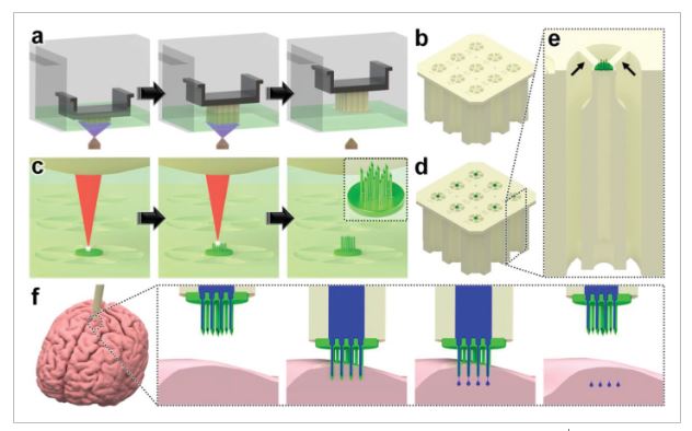
Conceptual illustrations of the hybrid additive manufacturing strategy for 3D microprinting hollow, high-aspect-ratio microneedle arrays (MNAs) for microinjection applications. a,b) Digital light processing (DLP)-based 3D printing of batch capillaries. a) A liquid-phase photocurable material is UV-crosslinked in designated locations in a layer-by-layer manner to produce a batch of arrayed capillaries comprising cured photomaterial. b) The DLP-printed batch of prealigned capillaries following the development process. c–e) “Ex situ direct laser writing (esDLW)” of MNAs directly atop—and fluidically sealed to—each DLP-printed capillary. c) A femtosecond pulsed IR laser is scanned to selectively initiate two-photon polymerization of a liquid-phase photocurable material in a point-by-point, layer-by-layer manner to produce MNAs comprising cured photomaterial. d) A batch array of MNA-capillary assemblies following the DLW-associated development process. e) Individual MNA-capillary assemblies within the array can be released on demand by manually severing the supporting structures (arrows). f) Example application of integrating MNA-capillary assemblies with nanoinjector systems to facilitate MNA-mediated simultaneous, distributed microinjections of target fluidic substances/suspensions into brain tissue.

Materials

Clear Microfluidics Resin V7.0a

2 Results and Discussion

Hybrid Additive Manufacturing of Hollow MNAs

The presented hybrid additive manufacturing strategy consists of two fundamental stages: i) DLP 3D printing of batch arrays of capillaries and ii) esDLW-based printing of the MNAs directly atop each capillary. DLP 3D printing is a vat photopolymerization approach in which a DLP projector is used to UV-crosslink a liquid-phase photocurable material in designated locations in a layer-by-layer manner to ultimately produce 3D objects composed of cured photomaterial.[62] Here, we leveraged DLP 3D printing to fabricate batches of arrayed capillaries in a single print run to overcome several drawbacks of recent esDLW approaches for printing 3D micro/nanostructured objects onto mesoscale fluidic components, such as micropiston-based microgrippers[63] and liquid biopsy systems[64] onto fluidic capillaries. First, the geometric control afforded by DLP 3D printing allows for each capillary to be designed with a variable OD to match the dimensions of the capillary base to those of the desired injector system. This capillary-specific geometric customization capability obviates the need for additional fluidic adapters and/or sealants (e.g., glues) often required to couple the mesoscale capillaries to macroscale fluidic equipment (e.g., injector systems).[63-65] Second, the outer dimensions of the batch array can be designed to support facile loading into the DLW 3D printer, which eliminates the time, labor, and costs associated with manufacturing and employing custom-built capillary holders typically needed for esDLW approaches.[63-65] Lastly, the ability to print all of the capillaries in predefined array locations—with uniform surface positions and rotational orientations—addresses critical deficits associated with the use of custom-built capillary holders that rely on undesired manual (e.g., by hand and/or eye) alignment protocols for each individual capillary.[65]

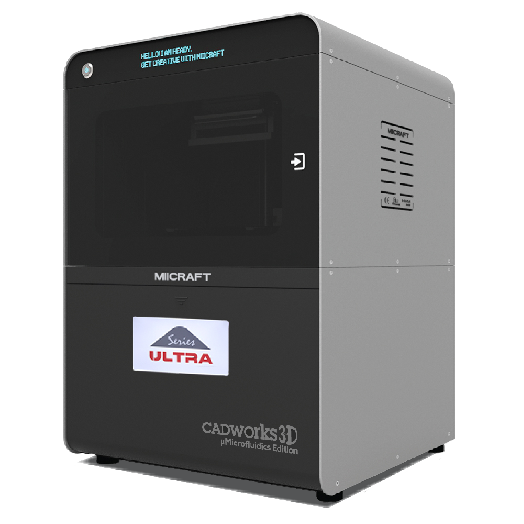
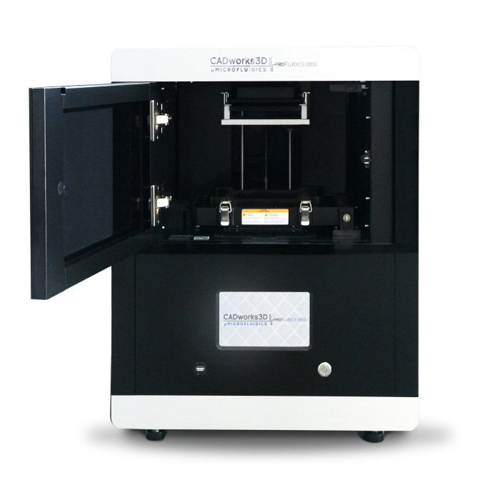
For DLP 3D printing of the batch capillary arrays, we used a Miicraft M50 microfluidics DLP 3D printer (CADworks3D, Toronto, ON, Canada) to fabricate two batches (i.e., 18 capillaries in total) per print run, which corresponded to a total print time of less than 45 min (Movie S1, Supporting Information). To enable direct integration with the nanoinjector system (MO-10, Narishige International USA, Inc., Amityville, NY), we designed each capillary with a consistent inner diameter (ID) of 650 µm, but with a variable OD that was set at 1.2 mm for the top 1.5 mm and then gradually increased to 2.4 mm for the remainder of the 10 mm length of the capillary (Figure S1, Supporting Information). Fabrication results revealed effective construction of the arrayed capillaries—each attached to the batch via five connecting structures (400 µm in width and depth; 1.5 mm in length) (Figure 2a,b). In addition, the outer dimensions of the overall batch resolved such that the print could be readily loaded into the multi-DiLL holder of the DLW system (Photonic Professional GT2, Nanoscribe GmbH, Germany) (Figure S2, Supporting Information) to facilitate esDLW-based 3D printing.

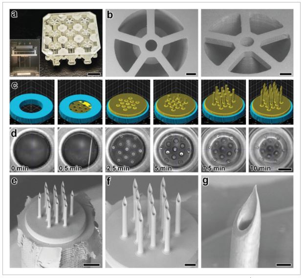
Fabrication results for DLP 3D printing of batch arrays of capillaries and esDLW-based printing of MNAs. a,b) DLP prints of batch arrays of capillaries. a) Photograph of a complete batch with nine arrayed capillaries. Scale bar = 5 mm. Inset shows two batches attached to the build plate directly after DLP 3D printing (see Movie S1 in the Supporting Information). b) Low-vacuum scanning electron microscopy (SEM) images of a representative DLP-printed capillary attached to the batch via five connecting structures. Scale bars = 500 µm. c,d) The esDLW approach for printing MNAs directly onto DLP-printed capillaries in a single print run. c) Computer-aided manufacturing (CAM) simulations and d) corresponding images of the esDLW printing process. Scale bar = 250 µm (see Movie 2 in the Supporting Information). e–g) Low-vacuum SEM images of representative fabrication results showing: e) an esDLW-printed MNA atop a DLP-printed capillary following release from the batch array (see Movie S3 in the Supporting Information); f) a magnified view of the MNA; and g) a magnified view of a single microneedle tip in the array. Scale bars = e) 250 µm, f) 100 µm, and g) 25 µm.

We designed the MNAs to include identical hollow microneedles—each with an ID of 30 µm, an OD of 50 µm, and a height of 550 µm—with needle-to-needle spacing of 100 µm (Figure S3, Supporting Information). For the esDLW printing process, we initiated the print with 50 µm of overlap with the top surface of the capillary to ensure bonding at the interface. Computer-aided manufacturing (CAM) simulations and brightfield images of a corresponding esDLW process for printing the MNA directly onto a DLP-printed capillary are presented in Figure 2c,d, respectively (see also Movie S2, Supporting Information). The total esDLW printing process was completed in ≈10 min. Following development, we retrieved target MNA-capillary assemblies from the batch by manually severing the five connecting structures (Movie S3, Supporting Information). Images of the released MNA-capillary assemblies captured using low-vacuum scanning electron microscopy (SEM) revealed effective alignment and integration of the esDLW-printed MNAs with the DLP-printed capillaries, without any visible signs of physical defects along the MNA-capillary interface (Figure 2e). In addition, images of the esDLW-printed MNA and needle tips suggest that the manual release process did not appear to affect MNA integrity (Figure 2f,g).

In Silico and In Vitro Investigations of MNA Mechanical Performance

The critical first steps of MNA-based microinjection protocols involve the effective puncture and penetration into a target medium (e.g., biological tissue), which can impart significant mechanical forces on the microneedles.[66] Thus, the potential utility of MNAs is predicated on their ability to successfully withstand such mechanical loading conditions. To evaluate this capability for the esDLW-printed high-aspect-ratio MNAs, we employed both numerical and experimental approaches to elucidate the mechanical performance of the MNAs. We performed finite element analyses (FEA) to provide insight into the mechanical failure behavior of the MNAs when subjected to a compressive load applied longitudinally with respect to the needles. The simulation results revealed that each arrayed microneedle exhibited a buckling-like deformation with the largest displacements observed around the midpoint of the heights; however, needles positioned in the outer region (i.e., the needles radially arrayed farthest from the center of the MNA) displayed larger deformations compared to those located in the more central array positions (Figure 3a). This behavior arises from the load distribution caused by the disc-like base of the MNA, which deforms more in its central region than its peripherical region, thereby allowing the centrally located microneedles to rigidly displace more in the axial direction than their outer-region counterparts. According to the stress–strain curve generated from the FEA compressive loading simulations (Figure 3b), the overall MNA exhibited an effective Young's Modulus (E) of 4.31 MPa and yield strength (σy) of 135 kPa. We also numerically modeled MNA mechanics associated with puncture into the brain tissue. By characterizing the nonlinear response at the interface between the tips of the microneedles and the brain substrate, we found that the forces associated with the needles located in the outer region were larger than those in the central regions (Figure S4, Supporting Information), which is in agreement with the compressive loading analyses (Figure 3a).

The critical first steps of MNA-based microinjection protocols involve the effective puncture and penetration into a target medium (e.g., biological tissue), which can impart significant mechanical forces on the microneedles.[66] Thus, the potential utility of MNAs is predicated on their ability to successfully withstand such mechanical loading conditions. To evaluate this capability for the esDLW-printed high-aspect-ratio MNAs, we employed both numerical and experimental approaches to elucidate the mechanical performance of the MNAs. We performed finite element analyses (FEA) to provide insight into the mechanical failure behavior of the MNAs when subjected to a compressive load applied longitudinally with respect to the needles. The simulation results revealed that each arrayed microneedle exhibited a buckling-like deformation with the largest displacements observed around the midpoint of the heights; however, needles positioned in the outer region (i.e., the needles radially arrayed farthest from the center of the MNA) displayed larger deformations compared to those located in the more central array positions (Figure 3a). This behavior arises from the load distribution caused by the disc-like base of the MNA, which deforms more in its central region than its peripherical region, thereby allowing the centrally located microneedles to rigidly displace more in the axial direction than their outer-region counterparts. According to the stress–strain curve generated from the FEA compressive loading simulations (Figure 3b), the overall MNA exhibited an effective Young's Modulus (E) of 4.31 MPa and yield strength (σy) of 135 kPa. We also numerically modeled MNA mechanics associated with puncture into the brain tissue. By characterizing the nonlinear response at the interface between the tips of the microneedles and the brain substrate, we found that the forces associated with the needles located in the outer region were larger than those in the central regions (Figure S4, Supporting Information), which is in agreement with the compressive loading analyses (Figure 3a).

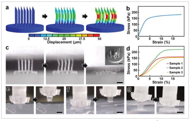
Numerical and experimental results for MNA mechanical characterizations. a,b) Finite element analysis (FEA) results for a) microneedle deformations and b) stress–strain curve corresponding to MNA mechanics under compressive loading conditions. c,d) Experimental results for MNA compression testing. c) Sequential images of the MNA during axial compression test. Inset shows an SEM image of an MNA following compressive failure. Scale bars = 250 µm (see Movie S4 in the Supporting Information). d) Stress–strain curve generated from compressive loading experiments (n = 3 MNAs). e–g) Sequential images of representative MNA penetration and retraction operations corresponding to hydrogels with agarose concentrations of: e) 2.4%, f) 5%, and g) 10%. Scale bars = 500 µm (see Movie S5 in the Supporting Information).

To experimentally examine the mechanical performance of the esDLW-printed MNA, we conducted two sets of puncture and penetration-associated studies. First, we performed axial compression tests with esDLW-printed MNAs (n = 3), which revealed buckling-type deformations of the microneedles with increasing loading until complete mechanical failure (Figure 3c and Movie S4, Supporting Information). From SEM images of MNAs following compressive testing, we observed several cases of complete fracture, but the majority of the arrayed microneedles remained intact with the caveat that the tips and the overall shapes of the needles exhibited plastic deformation (Figure 3c, inset). Quantified results for the stress–strain relationships for the esDLW-printed MNAs revealed an average E of 2.12 ± 0.35 MPa and σy of 155 ± 30 kPa (Figure 3d). Although these results provide insight into the upper boundaries of mechanical loading, compression testing using an impenetrable plate is limited in its direct relevance to microinjection applications that rely on microneedle penetration into a target medium. Thus, we also investigated the capacity for the esDLW-printed MNAs to puncture and penetrate into surrogate hydrogels with increasing concentrations of agarose that correspond to varying degrees of biologically relevant stiffness. In particular, we performed experiments with agarose concentrations of: i) 1.2% (E = 12.8 ± 1.1 kPa), which would support penetration into liver and breast tissue; ii) 2.4% (E = 27.5 ± 1.0 kPa), which is relevant to brain, heart, kidney, arterial, and prostate tissue; and iii) both 5% (E = 223 ± 14 kPa) and 10% (E = 268 ± 31 kPa), which are relevant to cartilage tissues (Figure S5, Supporting Information).[67-70] Experimental results revealed that the MNA successfully penetrated into the 1.2%, 2.4%, and 5% agarose gels; however, we observed buckling of the microneedles and failure to penetrate into the 10% agarose gel (Figure 3e–g and Movie S5, Supporting Information). These results suggest that the esDLW-printed MNA is sufficient for penetration into brain tissue as well as a variety of other tissues (e.g., liver, breast, heart, kidney, arterial, and prostate tissues), but alternative photomaterials (with stronger mechanical properties) and/or microneedles with geometrically enhanced strength (e.g., by increasing the OD) would be needed for microinjection applications involving target mediums with E in excess of 250 kPa.

In Vitro Microfluidic Interrogations of MNA-Capillary Interface Integrity

One of the most catastrophic failure modes for esDLW-based prints—whether for optical,[71] photonic,[72] mechanical,[73] or fluidic[63-65] structures—is the potential for the DLW-printed objects to detach from the meso/macroscale components on which they are additively manufactured. For biomedical MNA applications, the consequences of this type of failure could be particularly serious, such as an MNA detaching from the capillary while embedded in brain tissue following microinjection. To investigate the potential for this failure mode and, in turn, provide insight into the mechanofluidic integrity of the interface between the esDLW-printed MNAs and the DLP-printed capillaries, we performed microfluidic cyclic burst-pressure tests with the MNA-capillary assemblies. Initially, using an applied pressure set at 5 kPa, we gradually infused blue-dyed deionized (DI) water into the MNA-capillary assembly via the opposing end of the capillary (i.e., the side without the printed MNA) until the fluid began exiting the tips of the arrayed microneedles (Figure 4a and Movie S6, Supporting Information). Thereafter, we performed separate sets of cyclic burst-pressure experiments (n = 100 cycles per experiment) corresponding to applied pressures set at 100, 200, and 300 kPa (Figure 4b–d). Throughout the burst-pressure testing, we monitored the MNA-capillary interface under brightfield microscopy for visible signs of undesired leakage phenomena (e.g., fluid exiting at any point along the interface rather than out of the tops of the microneedle tips); however, we did not observe any instances of such flow behavior. Similarly, quantified results of fluid flow through the MNA-capillary assembly recorded during the burst-pressure tests did not exhibit any indications of burst events—i.e., large increases in flow rates after a certain point, despite the applied pressure remaining constant—nor signs of gradual leakage phenomena associated with the flow rates increasing from pressure cycle to pressure cycle over the course of the experiment. Rather, the flow rate magnitudes corresponding to the applied input pressures remained consistent throughout the burst-pressure experiments (Figure 4b–d), suggesting uncompromised fluidic integrity of the MNA-capillary interface for all cases examined.

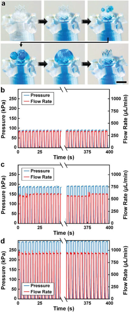
Experimental results for MNA microfluidic investigations. a) Sequential images during fluidic infusion. Scale bar = 500 µm (see Movie S6 in the Supporting Information). b–d) Quantified results for representative cyclic burst-pressure experiments (n = 100 cycles) corresponding to input pressures targeting: b) 100 kPa, c) 200 kPa, and d) 300 kPa.

Ex Vivo Mouse Brain Studies of MNA Penetration, Microinjection, and Retraction Functionalities

As an exemplar with which to interrogate the penetration, microinjection, and retraction capabilities of the esDLW-printed MNAs, we excised brains with intact dura mater from euthanized 6-month-old male mice (Wildtype C57BL/6 J, Jackson Laboratory) for experimentation ex vivo (Figure 5a). We performed three sets of experiments to elucidate these fundamental MNA functionalities. First, we investigated the ability to execute penetration and retraction operations (but not fluidic microinjections) with the MNAs as critical measures of performance with respect to three potential failure modes that would critically limit the efficacy of the esDLW-printed MNAs: i) the sharpness of the tips of the microneedles—governed by the resolution of the DLW 3D printer—is insufficient to puncture the brain tissue without inducing significant deformation of the brain; ii) the mechanical properties of the high-aspect-ratio microneedles lead to buckling and/or fracture of the microneedles prior to effective penetration into the brain tissue; and/or iii) the forces during the penetration or retraction processes fracture the microneedles, causing microneedles (or fragments of microneedles) to remain embedded in the brain tissue after retraction completion. To facilitate the penetration and retraction studies, we interfaced each MNA-capillary assembly examined with a nanoinjector system fixed to a stereotactic frame as a means to enable precise position control while optically monitoring the MNA-brain tissue interactions. Experiments performed with three distinct MNA-capillary assemblies (n = 3 penetration and retraction operations for each distinct MNA-capillary assembly) revealed that the MNAs could successfully puncture the brain tissue within 1 mm of total displacement from initial contact and, importantly, without any visible signs of mechanical failure during any of the penetration or retraction operations (Figure 5b and Movie S7, Supporting Information). Images of the MNAs (captured after completion of the retraction process) corroborated these results, without any indications of microneedle-associated failure modes (e.g., buckling or fracture) or MNA detachment from the capillary (Figure 5c).

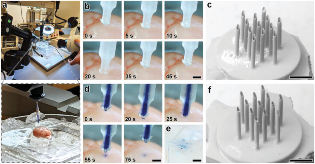
Experimental results for ex vivo MNA penetration, microinjection, and retraction operations using an excised mouse brain. a) Experimental setup including the MNA-capillary assembly interfaced with a custom-built nanoinjector and an excised mouse brain on ice. b,c) Brain tissue puncture and retraction results. b) Sequential images of MNA insertion into (≤20 s) and retraction from (≥20 s) the brain tissue. Scale bar = 1 mm (see Movie S7 in the Supporting Information). c) SEM image of the MNA after retraction from the brain tissue. Scale bar = 250 µm. d–f) MNA-mediated microinjection results. d) Sequential images of a representative MNA penetration, microinjection, and retraction process for a surrogate fluid (blue-dyed DI water) injected into brain tissue. Scale bar = 1 mm (see Movie S8, Supporting Information). e) Magnified view of the postinjection site. Scale bar = 250 µm. f) SEM image of the MNA following microinjection into the brain tissue. Scale bar = 250 µm.

After validating the penetration and retraction capabilities, we then initially investigated the microinjection functionality of the MNAs based on the ability to deliver a surrogate microfluidic payload into the brain tissue. In this case, we preloaded the MNA-capillary assembly with blue-dyed (1.5% Evan's Blue) DI water, and then interfaced the assembly with the nanoinjector (Figure 5a, expanded view) for control of both the MNA position and fluidic microinjection dynamics. Although the results for the cyclic microfluidic burst-pressure experiments performed in vitro (Figure 4b–d) suggested that the MNA-capillary interface should withstand the forces associated with microinjections into the brain tissue, we optically monitored the overall MNA-capillary assembly during the microinjection process for potential signs of undesired leakage via the interface. Akin to the tissue penetration and retraction studies, we used the stereotaxic frame to guide the descent of the MNA into the brain tissue (Figure 5d, top and Movie S8, Supporting Information). Following completion of the penetration process, we then used the pneumatically controlled nanoinjector to dispense the surrogate dyed fluid through the MNA-capillary assembly and, in turn, deliver the fluid into the brain tissue. Thereafter, we retracted the MNA from the brain (Figure 5d, bottom and Movie S8, Supporting Information), and then washed the surface of the injection site with phosphate buffered saline (PBS) to eliminate any residual surrogate fluid from the surface, such that the only remaining fluid was located beneath the tissue surface (Figure 5e). Throughout the microinjection process, we did not observe any undesired leakage phenomena (Movie S8, Supporting Information), with optical characterizations of the postinjection site indicating effective, distributed MNA-mediated delivery of the surrogate fluid well below the surface of the excised brain (Figure 5e). Furthermore, SEM images of the MNA-capillary assembly following tissue penetration, fluidic microinjection, and retraction revealed uncompromised structural integrity (Figure 5f).

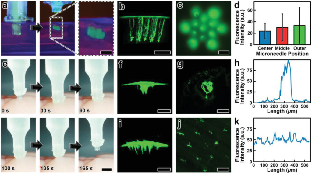
Lastly, we evaluated the microinjection performance of the esDLW-printed MNA compared to a conventional needle (Hamilton 33G) widely used for delivering therapeutics into brain tissue.[74] In this case, we used a suspension of fluorescently labeled nanoparticles (100 nm in diameter) as the surrogate microfluidic payload. As an initial positive experimental control for the esDLW-printed MNA, we performed microinjections (n = 3 MNAs) of the nanoparticle suspension into 0.6% agarose gel in vitro (Figure 6a and Movie S9, Supporting Information) and visualized the particle distributions using two-photon (Figure 6b S10) and widefield fluorescence microscopy (Figure 6c). We observed injected nanoparticles corresponding to each microneedle in the array—which included one microneedle in the center of the array, six needles arrayed radially in a middle region (150 µm from the center), and six needles arrayed radially in an outer region (260 µm from the center)—but to determine if microneedle array position influenced injection behavior, we analyzed the fluorescence intensities associated with each arrayed needle. Quantified results revealed that the fluorescence intensities were statistically indistinguishable, with no discernable difference for the microneedle injection sites between the center and either the middle (p = 0.66) or outer regions (p = 0.61), nor between the middle and outer regions (p = 0.72) (Figure 6d). Thereafter, we performed microinjections of the nanoparticle suspension into excised mouse brains using both the conventional needle and the esDLW-printed MNA (Figure 6e and Movie S10, Supporting Information). Two-photon fluorescence images of the injection sites revealed stark differences in the nanoparticle distributions associated with each needle system. In the conventional needle case, the nanoparticles accumulated tightly within the single needle track (Figure 6f,g). For example, quantified fluorescence intensity results revealed that the majority of the fluorescence signal was detected within an ≈150 µm region (Figure 6h). In contrast, MNA-associated microinjection sites exhibited a more homogeneous distribution of injected nanoparticles over a larger area (Figure 6i,j)—with particles detected at sites corresponding to each arrayed microneedle—resulting in a more consistent fluorescence signal along the length of the injection site (Figure 6k). These results suggest that MNAs offer an effective means to distribute fluidic payloads more uniformly over a larger area compared to conventional single-needle systems. In combination, these experimental results for MNA penetration, surrogate fluid/suspension delivery, and retraction functionalities using an ex vivo mouse brain provide an important foundation for the utility of the presented hybrid DLP-DLW-enabled MNAs for microinjection applications.

Experimental results for microinjections of fluorescent nanoparticles a–d) in vitro in 0.6% agarose gels and e–k) ex vivo using excised mouse brains. a) Sequential images of nanoparticle microinjection and retraction. Scale bar = 250 µm (see Movie S9 in the Supporting Information). b,c) Fluorescence images of the postinjection site captured using b) two-photon and c) widefield fluorescence microscopy. Scale bars = 250 µm. d) Mean fluorescence intensities of injection sites corresponding to microneedles in distinct array regions (n = 3 MNAs). Error bars = S.D. e) Sequential images of a representative MNA penetration, microinjection, and retraction process for a suspension of fluorescent nanoparticles injected into brain tissue. Scale bar = 1 mm (see Movie S10 in the Supporting Information). f–k) Postinjection results for fluorescent nanoparticles delivered via f–h) a conventional Hamilton 33G needle, and i–k) an esDLW-printed MNA. f,g,i,j) Fluorescence images of the postinjection site captured using two-photon fluorescence microscopy visualized in f,i) side and g,j) cross-sectional views. Scale bars = 250 µm. h,k) Quantified fluorescence intensities along the length of the corresponding cross-sectional views of the postinjection sites.

3.Conclusion

Microneedle-based microinjection protocols are essential to wide-ranging fundamental research and clinical applications across biological and biomedical fields, with MNAs providing numerous benefits over their single-needle counterparts in many scenarios.[75-77] Unfortunately, manufacturing-associated limitations have heretofore impeded researchers from leveraging the potential benefits of high-density MNAs comprising hollow, high-aspect-ratio microneedles at small length scales.[78-80] In this work, we introduced the concept of using esDLW to 3D print MNAs directly atop DLP-printed capillaries in batch arrays and demonstrated this approach by fabricating arrays of 50 µm OD, 30 µm ID, 550 µm tall hollow microneedles with 100 µm needle-to-needle spacing. Because the presented strategy is founded on two additive manufacturing technologies, the inherent geometric versatility can be harnessed to tailor both the DLP-printed capillaries and the esDLW-based MNAs to target experimental setups and applications. For the DLP-printed capillary, the shape and size need not be uniform along the length of the capillary as is the predominant case for conventional and/or commercially available fluidic capillaries. Here, for instance, we designed the OD of the base of the capillary to yield facile, direct integration with the nanoinjector, thereby circumventing the need for additional fluidic adapters or sealants. Similarly, although the presented design for the esDLW-printed MNAs included identical microneedles with dimensions based on a specific exemplar—i.e., fluidic microinjection into the cerebral cortex of a mouse brain—the high architectural control and submicrometer-scale resolution of DLW can be leveraged to customize the size, shape, and position of each individual microneedle in an array as desired (Figure S4, Supporting Information). For example, future efforts could increase the microneedle heights substantially to target different regions of the brain and/or additional animal models. Conversely, while this work centered on printing hollow microneedles (with 30 µm IDs) to support fluidic delivery operations, given the recent developments for the utility of solid MNAs in other cases, the presented strategy could also be extended to print MNAs composed of solid microneedles, such as those fabricated using DLW-compatible biodegradable materials,[81, 82] or potentially hybrid MNAs that comprise both hollow and solid microneedles.

The presented strategy also provides an important foundation for future academic and industrial translation through four pathways. First, in contrast to prior esDLW efforts, DLP-printing of the batch arrays of fluidic capillaries allows for facile loading into the DLW 3D printer, obviating the need for custom-built capillary holders as well as the time- and labor-intensive protocols required to manually load each individual capillary into such holders. Furthermore, because each capillary is printed in a designated array position with specified orientations, the setup for initiation of the esDLW-printing process is minimized, which could provide a promising avenue to scalable and automated production. Second, although we employed a layer-by-layer DLP printer to manufacture the batch arrays of fluidic capillaries, numerous vat photopolymerization approaches could be used instead to increase production speed, including continuous liquid interface production to print parts in minutes[83] and various volumetric 3D printing strategies to fabricate parts in tens of seconds.[84-86] Third, for esDLW-based printing of the MNAs, while the voxel size remained constant throughout the printing process with a scan speed of ≈120 mm s−1, future efforts can harness recent advancements for state-of-the-art DLW printers that can not only dynamically tailor the size of the voxel to target features but also allow for scan speeds up to 1,250 mm s−1 (e.g., with 5× objective lens configurations) in order to dramatically enhance print efficiency and speed. Lastly, recent improvements in the available build area for commercial DLW printers could be extended to print multiple MNAs simultaneously in a single pass (in contrast to the serial MNA printing strategy reported here), which would further increase the attainable production volume.

The numerical and experimental mechanical characterizations of the esDLW-printed MNA suggest that, in addition to brain tissue, the MNA described in this work could be used to facilitate microinjections for a wide range of additional biological tissues, including those associated with the liver, breast, heart, kidney, veins, arteries, and prostate.[67-70] For future efforts based on different injection targets with higher stiffness (e.g., E > 250 kPa), however, the inability of the presented MNA to successfully penetrate into the 10% agarose gel indicates that, for the current design, alternative photomaterials should be used for esDLW-based printing. In particular, researchers have reported DLW-compatible fused silica glass-based photomaterials,[87] which are now available commercially and would provide an order of magnitude increase in E of the fabricated MNAs. Alternatively, while we designed each microneedle with 10-µm-thick walls and 50 µm ODs, both dimensions could be readily increased to improve the mechanical strength. For excised mouse brains specifically, the ex vivo investigations in the current study revealed effective MNA-mediated penetration, microinjection, and retraction operations without any instances of microneedle-associated mechanical failures (e.g., buckling or fracture). In addition, throughout both in vitro microfluidic cyclic burst-pressure characterizations (with applied pressures in excess of 250 kPa) and ex vivo brain tissue experiments, the MNA-capillary interface exhibited consistent fluidic integrity, without any signs of undesired leakage phenomena or MNA detachment from the capillary.

We envision that future efforts could extend the methodology reported here to achieve novel MNA designs that remediate the deficits of single-needle injection strategies by expanding the delivery range via simultaneous, distributed microinjection. For example, as both in vitro and ex vivo experiments for MNA-mediated microinjections of nanoparticle suspensions revealed homogeneous distributions of implanted particles, such capabilities could offer new means to address the cell crowding challenges of SCT associated with single-needle delivery systems that contribute to low cell viability and, thus, limited therapeutic efficacy.[88-91] Such a pathway to improved SCT could hold distinctive promise for treating a diversity of medical conditions and neurodegenerative diseases, but further studies are needed to explore the potential for MNAs at this scale to enhance therapies that rely on fluidic microinjections—not only for stem cells, but also additional therapeutic payloads (e.g., growth factors and viruses for gene therapy)—into the brain. Nonetheless, given the vast diversity of scientific and clinical applications that are founded on microinjections and/or microneedles, the presented hybrid additive manufacturing strategy offers unique potential as an enabling technology for realizing entirely new classes of MNAs to advance scientific discovery and promote human health and well-being.

4.Experimental Section

Batch Capillary Array Fabrication via DLP 3D Printing

The computer-aided design (CAD) software, SolidWorks (Dassault Systèmes, France), was used to generate models of batch arrays of capillaries (Figure S1, Supporting Information). Models were exported as STL files and then imported into the CAM (slicer) software for the Miicraft M50 DLP 3D printer (CADworks3D, Canada) to define the print parameter settings (Table S1, Supporting Information). The batch capillary arrays were DLP-printed using Clear Microfluidics Resin V7.0a (CAdworks3D) with the layer height set to 50 µm. Following the DLP printing process, the build plate was removed and the prints were manually detached from the build plate using a razor blade. The prints were developed in methanol for ≈10 s and then methanol was perfused through each capillary to eliminate any residual resin from the interiors. After one additional rinse with methanol, the prints were washed with 90% isopropyl alcohol (IPA). The prints were then dried with pressurized air and postcured under UV light for 20 s (flipping the device after 10 s to cure both sides equally).

MNA Fabrication Atop the Capillaries via esDLW

The microneedle arrays—modeled using SolidWorks (Dassault Systèmes)—were designed with identical needles (ID = 30 µm; OD = 50 µm; height = 550 µm) and arrayed with 100 µm needle-to-needle spacing (Figure S3, Supporting Information). MNA models were exported as STL files and then imported into the CAM software, DeScribe (Nanoscribe), to define the print parameter settings (Table S2, Supporting Information), which included a hatching distance of 800 nm and a layer height of 2.5 µm. Initially, IP-Q photoresist (Nanoscribe) was dispensed directly atop the DLP-printed capillaries and the batch was then loaded into the Nanoscribe Photonic Professional GT2 DLW 3D printer (Figure S2, Supporting Information). For esDLW printing, the dip-in laser lithography (DiLL) mode was used with a 10× objective lens, a laser power of 27.5 mW, and a laser scanning speed of 120 000 µm s−1. The printing process was initiated with 50 µm of overlap with the top capillary surfaces. Following the esDLW process, the batch assembly (with MNAs printed atop the capillaries) was removed from the DLW printer for development. The prints were developed using propylene glycol monomethyl ether acetate (PGMEA) for 30 min and IPA for 5 min, and then dried using a gentle stream of N2 gas. Individual MNA-capillary assemblies were removed from the batch by manually severing the five connecting structures arrayed radially around each capillary (Movie S3, Supporting Information).

Finite Element Analysis (FEA)

Numerical simulations of the MNA compression test were performed using the commercially available software, ABAQUS/Standard (Abaqus Inc., Palo Alto, CA). Initially, the complete 3D CAD model of the MNA (i.e., including both the base and needles) was imported into the FEA software, and then the distinct material properties were set. Specifically, the MNA was modeled as a linear elastic homogeneous material (E = 250 MPa; ν = 0.49). The mesh was constructed using four-node, linear, 3D-stress-tetrahedra elements (ABAQUS element type C3D4H), and the accuracy was verified by mesh convergence. During all studies, the circular bottom surface orthogonal to the loading direction was modeled to be perfectly fixed. A static analysis (*STATIC step with NLGEOM = ON in ABAQUS) was conducted to characterize the nonlinear response and loaded the structure by linearly increasing the applied tip force. To characterize the nonlinear response at the interface between the needle tips and the brain substrate, the bottom surface of the cylinder mimicking the brain sample was modeled to be fully clamped while a displacement was applied to the MNA's cylindrical base. A surface-to-surface contact was defined between the brain substrate and the MNA needle tips. Both tangential and normal contact behaviors were defined. The MNA was modeled as a linear elastic homogeneous material, while the brain substrate was modeled as a hyperelastic Neo-Hookean material. To characterize the nonlinear response at the interface between the needle tips and the brain substrate, a dynamic implicit analysis (*DYNAMIC step with NLGEOM = ON in ABAQUS) was conducted.

MNA Mechanical Characterization

Mechanical testing on the MNAs was conducted using a Q800 Dynamic Mechanical Analysis (DMA) system (TA Instruments, New Castle, DE) equipped with a compression clamp. Samples were compressed at a rate of 0.1 N min−1 until the failure was confirmed via optical microscopy. Values for E and σy of MNAs were calculated from the linear region of the resulting stress-strain curve. To evaluate the puncture ability of the MNAs, hydrogels with different stiffness were prepared by mixing agarose gel powder in 1% PBS (Sigma-Aldrich, Saint Louis, MO) at four different concentration levels: 1.2%, 2.4%, 5%, and 10%. The solutions were heated to a boiling temperature and then cooled down until the hydrogels were set at room temperature. Before each MNA puncture, the top surface of the hydrogel was rinsed with PBS. The MNA was mounted on a stereotaxic manipulator, slowly inserted into the hydrogel samples, and optically monitored for any signs of failure.

Ex Vivo Mouse Brain Extraction and Experimentation

Brain tissues excised from 6-month-old male mice (Wild-type C57BL/6 J, Jackson Laboratory) were used for all ex vivo experiments. Each brain with an intact dura mater was excised within 10 min of euthanasia and stored in cold PBS on ice prior to testing. To maintain tissue integrity, the tissue samples were handled gently before and during the experiment. Each MNA-capillary assembly was interfaced with a custom-built nanoinjector (Narishige) and mounted on a stereotax with a digital display (#68807, RWD, China) to control the displacement and perform microinjections. In separate experiments, blue-dyed water and green fluorescent nanoparticles (505/515, 100 nm diameter, #F8803, Thermofisher) diluted with PBS were injected into the freshly dissected mouse cerebral cortex (or agarose gel) using either an MNA-capillary assembly connected to a micromanipulator (#MO10, Narishige) or a Hamilton syringe with a 33G needle connected to a motorized pump (#78–8130, KD Scientific, Holliston, MA). The injection depth was 500 µm with an extra 200 µm overshoot. The injection duration was ≈2 min for both MNA and Hamilton syringe-mediated injections. After injection with fluorescent nanoparticles, the fresh mouse brains were fixed with 4% paraformaldehyde for 2 d, rinsed, and mounted on glass slides for imaging under a two-photon microscope. These studies were performed in accordance with the National Institutes of Health (NIH) Guide for Care and Use of Laboratory Animals and the University of Maryland, School of Medicine, Animal Care and Use Committee.

Optical Characterizations

SEM images were captured using a TM4000 Tabletop SEM (Hitachi, Tokyo, Japan) under low vacuum, which allowed for imaging of uncoated samples. The mechanical tests were recorded using a Monocular Max 300× microscope objective and a 41MP USB C-Mount Industry Microscope Camera Set (Hayear Electronics Co. Ltd., Shenzhen, China). Brightfield microscopy during microfluidic testing was performed using an inverted microscope (Motic AE31, Motic, Canada) connected to a CCD camera (Moticam Pro 285B, Motic). For ex vivo microinjection experiments, the injection process was recorded using the Monocular microscope while the fluorescent images of the top view of the gel injection site were captured using a DMi8 automated fluorescence microscope (Leica Microsystems, Wetzlar, Germany). The 3D stack images of the injection sites were acquired using the Modular In Vivo Multiphoton Microscopy System designed by Janelia Research Campus, Howard Hughes Medical Institute. A 900 nm laser (≈5 mW) was used for excitation of the green fluorescent nanoparticles. The 3D stacks from the top of the brain to the bottom of the needle track were acquired at a step size of 2 µm under a water-immersion 25× objective (numerical aperture of 1.05, Olympus). Fluorescence emission was collected by two GaAsP photomultiplier tubes after being split by a dichroic mirror (560 nm, T560pxrxt, Chroma) with an emission filter green (510/84 nm, 84–097, Edmund) fluorescence. A similar acquisition setting was used for imaging the needle tracks in hydrogels injected with the fluorescent nanoparticles. Fluorescence images were processed and visualized with ImageJ (NIH, Bethesda, MD). BigDataViewer was used to adjust the tilting angle of the 3D stack for optimized visualization. For comparisons of needle-to-needle injection sites within the MNAs as well as injection distributions between the MNA and Hamilton injections, ImageJ was used to quantify the fluorescence intensities.

Statistical Analysis

Statistical significance was quantified via unpaired Student's t-tests, with two-tailed p values greater than 0.05 considered statistically indistinguishable. A minimum of three samples were used to quantify any means reported, with data presented in the text as mean ± standard deviation (S.D.).

Acknowledgements

The authors greatly appreciate the contributions of Olivia Young, Michael Restaino, and Chen-Yu Chen, as well as additional members of the Bioinspired Advanced Manufacturing (BAM) Laboratory and the William Bentley Laboratory. The authors appreciate the help and support of staff members at the University of Maryland Terrapin Works and the Micro/Nanofabrication Center at the Princeton Institute of Materials. This work was supported in part by the Maryland Robotics Center, the Center for Engineering Concepts Development (CECD), U.S. NIH Award Numbers 1R01EB033354-01, 1R03NS123733-01, 1R21AG077631-01, 1R03NS128459-01, 1R01EB019963, and F31DK129021, the Maryland Stem Cell Research Fund 2022-MSCRFL-5893, and U.S. National Science Foundation (NSF) Award Number 1943356. The content is solely the responsibility of the authors and does not necessarily represent the official views of the NIH. Correction added on 10th March 2023 after initial publication: The affiliation for P. Walczak was corrected.]

Conflict of Interest

The authors declare no conflict of interest.

3D-printed capillaric ELISA-on-a-chip with aliquoting

3D-printed capillaric ELISA-on-a-chip with aliquoting

Azim Parandakh, Oriol Ymbern,  William Jogia, Johan Renault, Andy Ng and  David Juncker

Sandwich immunoassays such as the enzyme-linked immunosorbent assay (ELISA) have been miniaturized and performed in a lab-on-a-chip format, but the execution of the multiple assay steps typically requires a computer or complex peripherals. Recently, an ELISA for detecting antibodies was encoded structurally in a chip thanks to the microfluidic chain reaction (Yafia et al. Nature, 2022, 605, 464–469), but the need for precise pipetting and intolerance to commonly used surfactant concentrations limit the potential for broader adoption. Here, we introduce the ELISA-on-a-chip with aliquoting functionality that simplifies chip loading and pipetting, accommodates higher surfactant concentrations, includes barrier channels that delay the contact between solutions and prevent undesired mixing, and that executed a quantitative, high-sensitivity assay for the SARS-CoV-2 nucleocapsid protein in 4×-diluted saliva. Upon loading the chip using disposable pipettes, capillary flow draws each reagent and the sample into a separate volumetric measuring reservoir for detection antibody (70 μL), enzyme conjugate (50 μL), substrate (80 μL), and sample (210 μL), and splits washing buffer into 4 different reservoirs of 40, 40, 60, and 20 μL. The excess volume is autonomously drained via a structurally encoded capillaric aliquoting circuit, creating aliquots with an accuracy of >93%. Next, the user click-connects the assay module, comprising a nitrocellulose membrane with immobilized capture antibodies and a capillary pump, to the chip which triggers the step-by-step, timed flow of all aliquoted solutions to complete the assay in 1.5 h. A colored precipitate forming a line on a nitrocellulose strip serves as an assay readout, and upon digitization, yielded a binding curve with a limit of detection of 54 and 91 pg mL−1 for buffer and diluted saliva respectively, vastly outperforming rapid tests. The ELISA chip is 3D-printed, modular, adaptable to other targets and assays, and could be used to automate ELISA in the lab; or as a diagnostic test at the point of care with the convenience and form factor of rapid tests while preserving the protocol and performance of central laboratory ELISA.

We kindly thank the researchers at McGill University for this collaboration, and for sharing the results obtained with their system.

Introduction

The enzyme-linked immunosorbent assay (ELISA) is utilized for the detection and quantification of proteins, antibodies, or antigens. The sandwich format with a capture antibody immobilized on the surface and a detection antibody applied in solution is used for assays requiring high sensitivity and specificity. Laboratory microplate ELISA still serves as a gold standard for assays and benefits from high sensitivity thanks to enzymatic signal amplification (down to sub-picomolar concentration for the best antibody pairs), quantitative results, standardized operations, off-the-shelf consumables, and a comparably high throughput thanks to the use of 96-well plates. Long incubation times and copious washing between different steps to reduce non-specific binding and assay background are critical to achieving high assay sensitivity. However, the ELISA suffers from several downsides, such as being laborious, lengthy (∼2–12 h depending on the protocol), requiring precise timing for each step, dependence on technical skills notably for adding and removing reagents (and thus susceptible to inter-operator variation) and necessitating a plate reader for signal readout.1,2

The miniaturization of ELISA has proceeded thanks to microfluidic lab-on-a-chip systems that can also automate the protocol.3,4 Microfluidics successfully reduced the consumption of reagents and the total assay time while preserving assay performance. However, whereas the chips are small, they rely on bulky peripherals such as syringe pumps3 or control motors,4 and a computer or an instrument for operation.5,6 Capillary phenomena and gravity have been harnessed to automate simple liquid manipulation, reducing or obviating the need for an external/active power supply.7–9 For instance, a disk-like microfluidic platform (powered by a combination of centrifugal and capillary forces)8 and a microfluidic siphon platform (powered by gravitational forces)9 have been developed to carry out the common steps of a conventional ELISA with reduced reagents consumption and assay time while preserving assay sensitivity. Yet, both examples require multiple precise pipetting steps and timed user interventions for operation.

Sandwich assays can also be performed at point-of-care using so-called lateral flow assays (LFAs), also called rapid diagnostics, and are used globally for pregnancy tests and COVID-19 (coronavirus disease 2019) diagnosis. LFAs replace the enzyme amplification with conjugated colorimetric particles (either gold nanoparticles or polystyrene beads) that become visible to the naked eye upon accumulation. LFAs are simple to use as they only require the application of the sample, which flows thanks to capillarity without the need for peripherals, and produce a test result within a few minutes. However, LFAs offer only qualitative yes-no results, their sensitivity is typically lower compared to that of laboratory ELISA and are not suitable for archival as the readout must be completed within a few minutes of the test, because otherwise, the result can be compromised.10–12 Enzymatic amplification has been implemented in the LFAs,13,14 for instance by using a microfluidic interface,14 to improve sensitivity. Yet, they cannot implement various fluidic handling tasks of common ELISA such as timed incubation of reagents and multiple rinsing steps between each incubation interval.

Paper-based microfluidics has been developed to introduce more advanced fluidic functions such as sequential delivery, additional rinsing step, and enzymatic amplification that collectively help improve assay sensitivity compared to LFAs.15–17 Sponge actuators that upon swelling connect or disconnect different parts of a paper-based microfluidic circuit, along with flow paths with different lengths and resistance, have been used to time the delivery of multiple reagents for completing a bona fide ELISA.17 However, these systems lacked the intermediate washing steps characteristic of classical ELISA, and undesired mixing of consecutive reagents occur at their mutual interface. Enzyme–substrate mixing may limit the potential for higher sensitivity as it could contribute to non-specific signal amplification.

Capillaric circuits (CCs) are capillary microfluidics in microchannels designed and built using capillaric elements which can automate liquid handling operations by pre-programming them structurally using capillary phenomena and powering them by capillary flow, without the need for peripheral equipment.18,19 Multiple CCs have been designed to perform and automate ELISA with new functionality including flow reversal,18 timing, reagent lyophilization,20 and portable readers,21,22 but they skip intermediate washing steps. Aliquoting a single solution into multiple reservoirs has been shown for a nucleic acid test.23 For an ELISA in a CC, multiple solutions including sample, buffer, and reagents must be serially delivered, and fluidically connected to effect fluid flow by hydraulic transmission of pressure differentials, which would subject them to unwanted mixing due to diffusion and/or convection, negatively affecting assay sensitivity and reliability.

The microfluidic chain reaction (MCR) introduces conditional initiation of capillary flow events, whereby event n is triggered after the preceding event n − 1 has been completed, and completion of n, in turn, initiates event n + 1; the condition is encoded using the so-called capillary domino valves.24 MCR can drive hundreds of sequential flow operations robustly, thus opening new opportunities for CCs. CCs and MCRs are susceptible to failure in the presence of surfactants that reduce surface tension and contact angles. Yet surfactants are essential ingredients to assays, and often 0.05% Tween 20 is used to prevent non-specific binding.25 In the initial MCR demonstration,24 only 0.0125% was used because higher concentrations led to corner flow and trapping of air bubbles19 and failure of stop valves. The initial MCR was used for a SARS-CoV-2 (severe acute respiratory syndrome coronavirus 2) antibody assay that could help determine the immune or vaccination status or detect prior infection, but which does not typically require high sensitivity needed for antigen assays where insufficient assay sensitivity often limits clinical usefulness.

User-friendliness is a critical feature for a device to be used at the point of need,26–28 and accurate aliquoting and volumetric consistency are essential to reliable immunoassays.29,30 Whereas in the lab they can be met using precision pipettes operated by technicians, they are difficult to achieve in a point-of-care setting. Both ELISA and the MCR CC introduced previously are dependent on precision pipetting. In particular, for the MCR chips,24 reagent loading occurred via miniature inlets that require precise positioning of the pipette, precise volumetric control and hence precision laboratory pipettes, and controlled pipetting rates to match the capillary flow rate of the reservoir being filled. LFAs for COVID-19 often include a dropper and instructions for delivering a precise number of droplets.31 Droppers are prone to occasional miscounting,31 while for more complex assays multiple solutions with different volumes are required that could not be serviced using droppers to be supplied and aliquoted with different volumes.

Here, we introduce the ELISA chip that automates ELISA protocol on a chip using an MCR CC while preserving the washing steps used in classical ELISA. The ELISA chip eases the pipetting procedure thanks to the automated aliquoting of solutions and can accommodate higher surfactant concentrations commonly used in immunoassays. Akin to measuring spoons that are used to size ingredients in cooking, measuring reservoirs with different volumetric capacities are used to aliquot reagents, buffer, and sample. Upon loading, solutions spontaneously fill their respective measuring reservoir, while an integrated capillaric aliquoting circuit (CAC) autonomously drains excess liquid from all reservoirs simultaneously, forming precise aliquots. We describe the capillaric circuitry and its components, and the step-by-step automated capillary flow operations of both aliquoting of all solutions and the sequential MCR-controlled ELISA protocol. We characterize the volumetric accuracy of aliquoting, the timing precision of delivery of the reagents for the ELISA, and the performance and limit of detection (LOD) of an assay for the detection of the SARS-CoV-2 nucleocapsid (N) protein spiked in buffer and 4×-diluted human saliva.

Materials

Results and discussion

ELISA chip

We designed a capillaric ELISA chip without a moving part that automates aliquoting of sample, reagents, and buffer, and autonomously executes an ELISA protocol by flowing eight solutions in sequence according to predetermined flow rates using an MCR (Fig. 1A and S1†). The solutions are delivered for the ELISA in the order of (i) sample, (ii) buffer, (iii) biotinylated detection antibody, (iv) buffer, (v) streptavidin poly-HRP (horseradish peroxidase), (vi) buffer, (vii) colorimetric substrate DAB (3,3′-diaminobenzidine) and (viii) buffer. The ELISA was developed for measuring the SARS-CoV-2 N protein in natural saliva and includes a strip of nitrocellulose membrane with a positive control line and a test line that will produce a permanent colorimetric signal proportional to the concentration of the N protein.

Fig. 1 3D-printed ELISA chip with aliquoting for SARS-CoV-2 N protein assay in saliva. (A) Picture of the chip with superposed process flow graphics. (i1) Reagents (R1–3) and (i2) washing buffer (W) are added to the inlets using disposable, low-precision pipettes shown in (B) and fill the measuring reservoirs by capillary flow; the washing buffer is split into four reservoirs automatically (W1–4). (i3) Addition of the sample brings the drainage capillary pump to a fluidic connection, initiating drainage of excess solutions from all inlets via the capillaric aliquoting circuit (CAC, see C), and producing (ii) final aliquots schematized by graduated tubes. (iii) Connection of the nitrocellulose strip triggers the ELISA via the sequential flow of sample, reagents, and washing buffer through the chip according to the propagation of the MCR. (iv) Following the enzymatic conversion of the substrate into a permanent line of a brown precipitate, the result can be read out by eye, and quantified following digitization. (B) Picture of a disposable pipette used to load the chip. (C) 3D design view of the ELISA chip with the structurally encoded capillaric elements without moving parts. The CAC is highlighted in yellow, and insets showcase (i) inlet barrier channel and supply/drainage conduit and air vent, (ii) reservoir outlet, outlet barrier channel, main assay conduit, and air vent (iii) sample inlet and reservoir, main drainage conduit and connection to supply/drainage conduit, and drainage capillary pump.

The need for the use of laboratory micropipettes is circumvented by integrating CAC into the chip which accepts the delivery of larger-than-needed volumes into the adequately sized inlets, followed by the spontaneous flow of the solutions via capillarity into serpentine measuring reservoirs for each solution. To complete the aliquoting process, the CAC removes excess volumes into a drainage capillary pump. The volume of each reservoir was set following assay optimization.

Simple squeeze pipettes, shown in Fig. 1B, can be used to load the chip while visually monitoring filling progression, and the measuring reservoirs form the aliquots (symbolized by graduated tubes) after draining excess liquid. The ELISA chip has five inlets servicing the eight reservoirs, three for the reagents, one for the buffer, and one for the sample, which need to be added in this order. The buffer is automatically split into four separate measuring reservoirs on the chip. The addition of the sample simultaneously fills the sample reservoir and initiates the drainage of excess volumes via the CAC. Next, upon click-connection of the main capillary pump, the step-by-step execution of the ELISA protocol is triggered, and the eight reservoirs chained by capillary domino valves are drained one by one as the MCR progresses. Finally, the signal is read out via the naked eye or using a scanner for quantification. A fluidic flow chart to explain the step-by-step manual user interventions and the ELISA chip's autonomous functions is provided in Fig. S2.

The ELISA chip is made by additive manufacturing using an off-the-shelf 3D printer and light-based photopolymerization, followed by a series of post-processing steps for a total time of ∼1 h (Fig. 2; see Experimental section for additional details).

Fig. 2 Additive manufacturing of ELISA chip and post-processing steps. The manufacturing includes (A) ELISA chip design in computer-aided design software, (B) digital light processing-based 3D printing, (C) rinsing with isopropanol (IPA) to remove uncured resin, (D) drying under a stream of pressurized nitrogen gas (N2), (E) 1 min UV curing, (F) 10 s air plasma treatment and (G) sealing with a microfluidic tape with cut-out openings for servicing sample, buffer, and reagent inlets.

Step-by-step loading and aliquoting

The ELISA chip loading and aliquoting are shown in Video S1.† Using a low-precision pipette (Fig. 1B), the user first deposits each reagent in the respective inlet in an arbitrary order with an excess of solution. The three serpentine reservoirs for the detection antibody, streptavidin poly-HRP, and DAB solutions have nominal measuring volumes of 70, 50, and 80 μL, respectively. Fig. 3A and B show the loading of the detection antibody and are representative of the other reagents. Capillary flow fills the reservoir up to the trigger valve at the empty outlet barrier conduit, while excess solution remains in the inlet and fills the trigger valve connecting to the conduit at the inlet (called inlet barrier channel) that is part of the CAC (see Fig. 1C). Next, the washing buffer is delivered to the common inlet to the right of the ELISA chip and flows by capillarity through the supply/drainage conduit into the four washing buffer measuring reservoirs with a nominal volume of 40, 40, 60, and 20 μL (Fig. 3C). The buffer simultaneously fills the main assay conduit, which is supplied by the vertical channel adjacent to the buffer inlet. The buffer distribution and splitting simplify chip loading as only one buffer solution needs to be added. However, the chip design imposes contact between buffer and reagents both at the inlet and outlet of the reagent reservoirs which could lead to unwanted mixing by diffusion and convection between various solutions.

Fig. 3 ELISA chip loading, filling into measuring reservoirs, and drainage of excess liquid by the CAC. Most figures show the part of the chip outlined by the dashed rectangle in Fig. 1C. (A and B) Loading of the detection antibody reagent into the inlet followed by capillary flow into the measuring reservoir and stop of the liquid at the capillary stop valves located next to the inlet and at the outlet. Loading of the other two reagents, i.e., streptavidin poly-HRP and DAB, follows the same procedure. (C and D) Loading of buffer in buffer inlet and splitting into the buffer reservoirs supplied by the supply/drainage conduit. (E–H) Sample loading with the filling of the sample reservoir and simultaneous triggering of the drainage of all excess solutions on the chip via the CAC. See Video S1† and text for further details.

Suppressing unwanted mixing and bubble trapping

We isolated each of the reagents measuring reservoirs to prevent unwanted mixing between them and/or the sample prior to assay completion. We equipped them with two diffusion barrier channels located upstream (at the inlet) and downstream (at the outlet) of each reagent reservoir. By isolation, we suppress undesired preliminary mixing of reagents that could affect assay performance and reproducibility during both aliquoting (i.e., filling and excess volume drainage), and subsequent ELISA sequential delivery (e.g. premature reaction between enzyme and colorimetric substrate DAB could lead to unwanted background signal). Because diffusion will occur for a long time at the outlet of each reservoir, and for almost the entire assay duration particularly for the DAB solution, the last reagent to flow in the ELISA protocol, a long diffusion barrier is needed. By implementing diffusion barrier channels, we increase the distance between ELISA reagents to prevent premixing that could occur by both diffusion and/or convection (e.g. small convective flows due to evaporation). The outlet barrier channel was designed with a U-turn and a separation length between the outlet of the reservoir and the main assay conduit with a length of 13–17 mm. The characteristic one-dimensional diffusion time is given as t = L2/D with L = length, D = diffusion constant, and t = time.32 For an IgG antibody with D ≅ 36 μm2 s−1 and DAB with D ≅ 570 μm2 s−1 (calculated by the Stokes–Einstein law for diffusion),32 the time for diffusion across 10 mm is ∼16 days and ∼1 day, respectively. In our case, the functional connection connecting the reservoir and the barrier forms a constriction,24 hence the diffusion time would be further increased relative to the calculation. The diffusion barriers thus ensure that no unwanted mixing occurs among reagents during the ELISA.

The inlet and outlet barrier channels form a separation between each reagent reservoir and the supply/drainage conduit (upstream), and main assay conduit (downstream) respectively. Both barrier channels remain empty during the autonomous filling of the reagents due to the action of trigger valves (see Fig. 3A), and autonomously fill by buffer after buffer injection (Fig. 3D). The inlet of the inlet (upstream) barrier conduit is located to the left of the reagent reservoir and branches out from the serpentine buffer reservoir, close to the outlet of the buffer reservoir. Upon reaching the branching point, capillary flow filling the buffer reservoir immediately branches into the barrier channel and fills it up to the extremity, which forms a dead-end. To prevent bubble trapping, an air vent is included that is connected to the channel via four stop valves, including three positioned upstream of the dead-end. At the reservoir outlet, the outlet barrier channel, which forms an extension to the buffer reservoir, is similarly filled by the buffer. However, the buffer reservoir to the right of the reagent channel supplies the corresponding outlet barrier channel and fills only after the buffer reservoir is filled completely (Fig. 3D bottom close-up, Video S1†). Akin to the inlet barrier channel, the extremity of the outlet barrier channels also forms a dead-end and is connected by three stop valves to a venting opening. Note that the design ensures that only pristine buffer fills each of the buffer measuring reservoirs. The inlet and outlet barrier channels are empty as the buffer starts flowing, and hence there is no contact or mixing between the reagents and the buffer flowing into the reservoirs.

The provision of multiple venting connections/stop valves is needed to accommodate liquids with low surface tension such as buffer containing a surfactant that is used in ELISA (e.g., Tween 20) and other assays. Low surface tension liquids have a lower contact angle than water (which has a high surface tension), which induces corner flow preceding the main filling front. The corner flow reaches the extremity of the conduit before the main filling front and can thus clog small air vents located at the extremity of dead-end channels before all the air can escape (see Fig. S3†). Upstream connections to the vent allow air to escape even after corner flow reaches the dead-end and here prevent air bubbles from being trapped. For the ELISA chip, we evaluated the chip fluidic functionality under Tween 20 concentrations of 0.0125%, 0.025%, 0.05%, and 0.1%, and because of occasional failure at 0.1%, limited it to 0.05% for subsequent experiments.

Excess volume draining

Drainage of the excess volumes is initiated by supplying the sample to the sample inlet (Fig. 3F). The sample inlet is connected to both the sample measuring reservoir and the main drainage conduit, both filling simultaneously by capillary flow. The outlet of the sample reservoir connects to a now pre-filled outlet barrier channel supplemented with an air vent to permit complete filing. The sample flowing into the main drainage conduit also initiates drainage of the excess volumes by triggering a trigger valve connecting the filled supply/drainage conduit to the main drainage conduit, and subsequently flowing to the drainage capillary pump, all part of the CAC. Initially, most of the drainage flow is supplied by the sample owing to excess solution in the sample inlet, the absence of a retention capillary pressure, and lower flow resistance. Once the sample inlet is emptied to the point where only corners remain filled, the drainage flow rates from the inlets containing excess buffer and reagents increase. The inlet barrier channel, in addition to minimizing the diffusion between the main drainage conduit and each reservoir, also forms the fluidic connection through which the excess reagent is drained from each reagent inlet.

Flow path routing during drainage

Whereas conceptually simple, in CCs, drainage must both be triggered and stopped without external intervention. In addition, multiple possible drainage paths exist when the circuit is operating in the absence of active valves to close off sections of the circuit, yet to avoid unwanted mixing and drainage of solutions in the reservoirs, the liquid flow must flow through a pre-designed flow path, Fig. 4A. In the desired path, the excess reagents flow from the common inlet to the drainage capillary pump as follows: reagent inlet → inlet barrier channel → supply/drainage conduit → main drainage conduit → drainage capillary pump. To facilitate flow and favor this fluidic path while preserving other capillaric functionality, we included 4 parallel connection conduits (0.1 × 0.2 × 0.75 mm3) between the inlet barrier channel and the supply/drainage conduit (Fig. 1C close-up i), which yielded an overall flow resistance of 135 Pa s mm−3 for path i.

Fig. 4 Drainage of excess volumes via the CAC. (A) The flow path for draining excess volumes in sample, reagent, and buffer inlets is shown with the black arrows. (B) In addition to the desired flow path i, three alternative, parasitic paths ii, iii, and iv are schematized using colored arrows. Drainage of reagent via a parasitic flow path could lead to mixing with other solutions and jeopardize the function of the ELISA chip. The design minimizes parasitic flow by ensuring that their flow resistance is much higher because they are longer and if necessary, sections with a small cross-section (and therefore a high flow resistance) are included. Note that in panel B, all flow paths are shown for only one reagent, and the same exist for other reagents as well.

For each reagent inlet, three unwanted, leaky flow paths exist, as illustrated for the detection antibody in Fig. 4B. Flow through any of the parasitic paths should be disabled as they would result in unwanted reagents mixing and/or deviation from the pre-programmed volumes. Path ii proceeds from reagent inlet → inlet barrier channel → washing buffer reservoir → supply/drainage conduit, and path iii from reagent inlet → reagent reservoir → reagent outlet barrier channel → washing buffer reservoir → supply/drainage conduit to the main drainage conduit and drainage capillary pump. Both paths would result in reagents flowing into, and mixing with, the washing buffer in the adjacent reservoirs. To impede drainage through path ii, the resistance at the inlet of the inlet barrier channel as well as that of the corresponding washing buffer reservoir was increased, resulting in overall flow resistance of 250 Pa s mm−3 for path ii. Likewise, to impede drainage through path iii, the resistance at the inlet of the outlet barrier channel as well as that of the corresponding washing buffer reservoir was increased, thereby the overall resistance of path iii was 550 Pa s mm−3.

Path iv follows the reagent inlet → reagent reservoir → reagent outlet barrier channel → main assay conduit → sample outlet barrier channel → sample reservoir → sample inlet → main drainage conduit → capillary drainage pump (Fig. 4B, path iv), with an overall resistance of 700 Pa s mm−3. This drainage path would lead to mixing with the sample, yet the last part of it being in charge of the excess drainage of the sample. This path only exists until the point where the excess sample is drained to the drainage capillary pump through the main drainage conduit (with an overall resistance of 50 Pa s mm−3) and is disconnected from the sample reservoir as the inlet is emptied.

Here we discussed the overall flow resistance of each of the four paths, but the parasitic flow is governed by the difference between the point where a given parasitic path splits from the drainage path i to the point where it merges again, which is a shorter distance. The ratio of flow resistance for the split section between path i, and each of paths ii, iii, and iv was calculated to be 7.8, 8.4, and 6.9 times higher respectively (Table S1†). Path iv is only active for a short time, and thus only contributes marginally. This design hence ensures that most of the excess volume will flow through path i.

The automated ELISA protocol

The ELISA is initiated by the user click-connecting the main capillary pump to the chip (Fig. 5A), which wicks liquid from the CC and the reservoirs, and initiates the MCR that propagates from one reservoir to the next via the capillary domino valves that chain the reservoirs24 (Video S2†). Briefly, the first reservoir is the sample reservoir that is capped by a retention burst valve (RBV) with a nominal capillary/burst pressure of −200 Pa (i.e., it will burst when the negative sucking pressure in absolute value is >200 Pa), which quickly bursts and results in draining of the reservoir. Air drawn in from the outside replaces liquid, and once all liquid is displaced, the capillary domino valve that forms an air link to the next reservoir is now connected to the outside via the just-emptied reservoir. At the top of the buffer reservoir, there is another RBV (here with the nominal capillary pressure of −215 Pa), which in turn bursts, leading to the draining of the first buffer reservoir, and in turn, opening the air link to the next (reagent) reservoir, and so on. The sequence of flow is thus sample, buffer, detection antibody, buffer, streptavidin poly-HRP, buffer, DAB, and buffer (Fig. 5B–F). Drainage of the main assay conduit is not controlled via the MCR because the chip lacked space for an additional capillary domino valve. Instead, we implemented an additional RBV with a nominal burst pressure of −550 Pa. That is the RBV with the highest threshold within the CC, and hence the last one to burst. The ELISA chip illustrates the possibility of combining an MCR with an RBV to control the sequence of liquids flowing through an assay conduit. Upon draining the main assay conduit at the last step, the main capillary pump and therefore the nitrocellulose membrane, is fluidically disconnected from the microfluidic chip to complete the ELISA.

Fig. 5 MCR progression of the ELISA chip to complete ELISA steps. (A) Click-connecting the main capillary pump to the chip (the region indicated by the black circle and arrow) triggers (B–G) sequential delivery of the sample, reagents, and corresponding washes to the sensor. Black arrows indicate the direction of flow. The black rectangle in panel A shows the small serpentines implemented in the ELISA chip to avoid mixing the sample with other reagents due to evaporation-induced backflow during sample delivery.

ELISA chip over-loading capacity and overflow

We evaluated the volumetric operational window of the ELISA chip that preserves aliquoting and overall ELISA chip functionality. We analyzed the video of four ELISA chips loaded using precision pipettes with known volumes of sample, reagents, and buffer, determined the minimum volume required to fill the measuring reservoirs, tested a range of excess volumes, and verified flow functionality while also monitoring unwanted mixing.

The nominal aliquot volume corresponds to the capacity of the measuring reservoir. However, in practice, some additional volume is needed to account for dead volumes in the chip. Conversely, if the inlets are overfilled, leakage into other parts of the chip could occur. We verified the nominal aliquoting accuracy by mapping the levels of the measuring reservoirs filled with food dyes after aliquoting was completed, and calculating the volumetric error by image analysis (see Experimental and Fig. S4† for detailed explanation). For the sample, the nominal aliquot volume is 210 μL but at least 300 μL is required because the sample triggers the CAC (as explained above). As this ELISA chip is designed for saliva, which was collected in an amount of 1 mL per individual, the additional volume requirement could be accommodated easily. We verified that the chips preserved their functionality and nominal aliquoting accuracy for a volume of 400 μL (maximum tested). Within the 300–400 μL range, the nominal accuracy of sample aliquoting was 99.5% with the coefficient of variation (CV) of 1.1%.

In the case of detection antibody, streptavidin poly-HRP, and DAB, the nominal aliquot volume is 70, 50, and 80 μL respectively, while loading the chip with a micropipette showed that at least an extra of ∼1 μL (for a total of 71, 51, and 81 μL, respectively) is needed to ensure complete filling of each reservoir with desired flow rate and without bubble entrapment. The maximum volumes that reagent inlets could accommodate while avoiding pre-mixing of reagents with buffer were 110, 90, and 120 μL for the detection antibody, streptavidin poly-HRP, and DAB, respectively. Under these conditions, the nominal accuracy of aliquoting was found to be 99.7 (CV = 2.1%), 93.4 (CV = 1.5%), and 99.9% (CV = 3.5%) respectively. In a case that overloading exceeds the maximum volumes, the chip will continue to function, but some part of the excess may spill into other reservoirs, which was observed when loading 140 μl of detection antibody led to spilling into the adjacent buffer reservoir (Fig. S5†).

For the washing buffer, ∼300 μL is needed to fill all washing buffer reservoirs as well as the supply/drainage conduit, inlet/outlet barrier channels, and main assay conduit. We tested its operation for a volume of up to 400 μl, successfully. Within this operating range, the buffer was reliably aliquoted into the four reservoirs of 40 μL, 40 μL, 60 μL, and 20 μL with a nominal accuracy of 98.7, 97.4, 98.3, and 94.7%, respectively, all with the CV of <1%. The results are summarized in Table 1. Considering these values, the ELISA chip outperforms the bulky pipetting robots utilized in laboratory ELISA, and indicates superior performance over the previously developed microfluidic devices while requiring significantly less user intervention.29,30 The computed tomography data provided in our previous study also confirm the high dimensional/volumetric precision of 3D-printed CCs with CV values of ≤3.9% in width and ≤1.2% in depth for the range of 400–1000 μm.24 It should be noted that due to the dimensional precision, the error in accuracy can be compensated by fine-tuning the length of a corresponding reservoir to adjust the volume.

Flow timing

We characterized the reliability of the timing of the ELISA protocol by measuring the duration of each step pre-programmed into the ELISA chip. The timing of the assay steps is an important parameter when considering the accuracy and reproducibility of ELISA. We analyzed the video of four ELISA chips loaded with assay reagents spiked with food dye colors for visualization purposes. Table 1 summarizes the draining/delivery duration for the sample, reagents, and buffer. Remarkably, we found the timing to be reproducible within a CV of 3.5% which confirms print-to-print precision on the smallest conduits which have a remarkably high flow resistance relative to large conduits, and where imprecision could thus disproportionally affect flow timing. We consider these results, both for the volumes and incubation times, excellent for a capillary-driven microfluidic system and suitable for conducting ELISA. Sequential delivery of all solutions takes ∼1.15 h. To reduce the effect of evaporation-induced backflow and the resultant mixing of the sample with other reagents, particularly during the ∼25 min of sample draining, the size and length of the main assay conduit were expanded (see serpentines in the main assay conduit in Fig. 5A).

SARS-CoV-2 N protein ELISA

To evaluate the performance of the ELISA chip, we used it to run a saliva-based SARS-CoV-2 N protein assay. We performed an in-depth optimization process including testing various concentrations of capturing antibody, detection antibody, streptavidin poly-HRP, and Tween 20 as well as the extent of saliva dilution on the minimum detectable signal and assay background. In particular, we observed that increasing Tween 20 concentration improved the assay background, with 0.05% and 0.1% concentrations having comparable performance (Fig. S6†). Saliva dilutions of 1×, 2×, 4×, and 10×, were tested, and 4× was selected as it eased flow through the nitrocellulose membrane, preserved a low assay background, and yielded good assay-to-assay reproducibility without significantly compromising sensitivity (see Table S2† for a summary of the optimization process).

Akin to classical microplate ELISA, the ELISA chip allowed for the implementation of enzymatic amplification that necessitates a two-step process (i.e., the addition of enzyme, followed by the substrate) which is not possible for the common LFAs that are typically carried out in one-step. DAB is the substrate used here which is chromogenic and oxidized in the presence of HRP, forming a brown precipitate at HRP locations. Whereas in laboratory ELISA the assay produces a colored solution, here it forms a precipitate on the paper strip which can be read out by the naked eye or digitized with a scanner.24 While the read-out time for both ELISA and LFAs is limited to a window of a few minutes, the precipitate in the ELISA chip is stable and can be read out later, thus potentially also serving as an archival record.

We generated binding curves by spiking-in N protein of SARS-CoV-2 across 6 orders of magnitude of dilution from 1 to 106 pg mL−1 in 4×-diluted pooled human saliva and ELISA buffer. Fitting the experimental data using a 4-parameter logistic regression, we obtained an LOD of 54 pg mL−1 and 91 pg mL−1 for the N protein in buffer and 4×-diluted pooled saliva, respectively (Fig. 6). The difference in LOD between buffer and saliva is due to the use of saliva as the diluent in the saliva binding curve, which leads to a higher background signal and greater variation than buffer alone. The small dilution of human saliva together with the high sensitivity of the assay is a practical advantage of the developed ELISA-on-chip given the higher performance needed for reliable COVID-19 diagnosis based on saliva testing.33

Fig. 6 Calibration curves of the SARS-CoV-2 N protein assay enabled by the ELISA chip. Different concentrations of SARS-CoV-2 N protein were spiked in ELISA buffer or 4×-diluted pooled saliva. The resultant time-insensitive colorimetric signals were then captured by a regular scanner and yielded a binding curve that was fitted with a 4-parameter logistic regression. The number of replicates for each concentration is 3 for each calibration curve.

We benchmarked the ELISA chip against two commercially available microplate-based ELISA for SARS-CoV-2 N protein detection (SinoBiological, Inc. and RayBiotech Life, Inc.). These ELISA kits use blood serum as the sample and have a time-to-result of ∼5 h with an LOD of 35 pg mL−1 and 70 pg mL−1, respectively, as reported by the manufacturer's protocol (Table 2). Note that the LODs of these serum ELISA were established based on a binding curve using buffer, and are thus comparable to the ELISA chip LOD for buffer; besides, RayBiotech calculated the LOD based on 2 × SD (standard deviation) above the blank instead of the widely used 3 × SD. The LOD of the ELISA chip rivals one of the classical ELISA kits while being four times faster with less hands-on time and no time-sensitive manipulations of liquids, and in a format that is compatible with the point-of-care setting.

A study compared the performance of seven LFA rapid antigen tests for N protein spiked in phosphate buffer saline.34 The tests notably included the widely used Abbott Panbio COVID-19 Ag Rapid Test and the Roche-SD Biosensor SARS-CoV Rapid Antigen Test. The most sensitive one was reported to be the R-Biopharm RIDA QUICK SARS-CoV-2 Antigen Test which yielded a line visible to the naked eye for a concentration as low as 2.5 ng mL−1.34 The LOD of the ELISA chip is ∼50 and ∼25 times higher than this LFA test in buffer and 4×-diluted pooled saliva, respectively.

Conclusions and future work

We presented an integrated ELISA chip that miniaturized and automated an ELISA-on-a-chip using capillarics and an MCR with an encoded aliquoting function, enabling the ELISA chip to be serviced with disposable pipettes. The ELISA chip generated aliquots with various volumes and timed the assay steps both within the CV of ≤3.5%, rivaling the common pipetting robots utilized in laboratory ELISA and other automated microfluidic ELISA.29,30 The ELISA chip could operate with 0.05% Tween 20 commonly used in assays. The LOD of the ELISA chip for the SARS-CoV-2 N protein in 4×-diluted saliva was 91 pg mL−1, in line with classical microplate ELISA and outperforming conventional lateral flow assays by ∼25×.

The ELISA chip could be 3D-printed and assembled in less than 1 h, and ∼1200 chips were manufactured as part of this work. ELISA chips were designed with superficial channels only and may thus be adaptable to mass production by injection molding with much lower mass manufacturing costs than 3D printing.

In the future, the chip may be validated with patient samples in retrospective and possibly prospective studies. The ELISA-on-chip introduced here will be particularly attractive for point-of-care applications where higher sensitivity than an LFA is needed while a longer assay time can be tolerated. Shortening assay time and further simplifying operations by pre-drying reagents and rehydrating them with a buffer solution20–22 would further increase the usefulness of the ELISA chip. A more systematic optimization to accommodate higher surfactant concentrations might expand the range of assays that could be automated on the chip. Finally, the effect of temperature, which is known to modulate the enzymatic turnover, will need to be studied and accounted for prior to clinical use. Following these improvements, ELISA Chips could be deployed at the point-of-need and used by non-experts, and using a cell phone for imaging and quantifying the assay results,21,22,24 quantitative, point-of-care tests with the performance of a central laboratory ELISA become available for everyone.

Experimental

ELISA chip fabrication and preparation

The chips were designed in AutoCAD (Autodesk), exported as “STL” files, and printed via an automated stereolithography 3D printer with the LED wavelength of 405 nm (Pr 110, Creative CADworks, Concord, Canada) using a monocure 3D rapid clear resin (Monocure 3D, NSW, Australia) with the following printing parameters: exposure time per layer: 2.5 s (10 s for the base layer); transition buffer layers: 2; layer thickness: 20 μm; printing delay: 1 min; and gap adjustment: 0.1 mm. Once printed, the chips were rinsed with isopropanol (Fisher Scientific, Saint-Laurent, Quebec, Canada) to wash away uncured resin, dried under a stream of pressurized nitrogen gas, cured for 1 min in a UV lamp (CureZone; Creative CADWorks; Concord; Canada), plasma treated for 10 s at 100% power (PE50 plasma chamber, Plasma Etch, Carson City, USA), and sealed with a microfluidic diagnostic tape (catalog number: 9795R; 3M Science. Applied to Life.™, Ontario, Canada).

A strip of Whatman CF4 paper (Cytiva, Marlborough, Massachusetts, United States) was clamped between 2 absorbent pads (Electrophoresis and Blotting Paper, Grade 320, Ahlstrom-Munksjo Chromatography, Helsinki, Finland) from the back end to collectively serve as the capillary pump. For the main capillary pump, a strip of Vivid™ 120 lateral flow nitrocellulose membrane (catalog number: VIV1202503R; Pall Corporation, Port Washington, USA) was clamped between the same absorbent pads from the back end and to a G041 glass fiber conjugate pad (Millipore Sigma, Oakville, Ontario, Canada) from the front end to facilitate connection to the chip.

Nitrocellulose membrane

The strips of Vivid™ 120 lateral flow nitrocellulose membranes were designed in AutoCAD with the dimensions of 5.2 mm wide and 12 mm long and cut using the Silhouette Portrait paper cutter (Silhouette, Lindon, USA). Membranes were stripped with a 5 mm-wide test line of SARS-CoV-2 N protein mouse monoclonal antibody (catalog number: 40143-MM08; Sino Biological, Inc., Beijing, China) at the concentration of 1 mg mL−1 and a 5 mm-wide control line of bovine serum albumin (BSA)–biotin solution at the concentration of 50 μg mL−1, both delivered using a programmable inkjet spotter (sciFLEXARRAYER SX, Scienion, Berlin, Germany). The membranes were dried for 1 h at 37 °C and blocked by dipping into the blocking buffer solution (1% BSA and 0.1% Tween 20 in PBS) until completely wet, followed by shaking on a rocker for 60 min at 75 rpm. The membranes were then retrieved, dried in an oven for 1 h at 37 °C, and stored with a desiccant at 4 °C until use on the next day.

SARS-CoV-2 N protein ELISA

Fresh saliva specimens were collected from three individuals using oral cotton swabs (Salivette, Sarstedt, Numbrecht, Germany) with their informed consent. The collected saliva samples were then pooled at a 1 : 1 : 1 ratio, filtered through a 0.22-micron filter, and diluted by a factor of 4 in the ELISA buffer solution (0.1% BSA and 0.05% Tween 20 in 1× PBS). The sample solutions were prepared by spiking SARS-CoV-2 N protein (catalog number: 40588-V08B; Sino Biological, Inc., Beijing, China) at the concentrations of 0, 1, 5, 10, 50, 102, 103 104, 105, and 106 pg mL−1 in either the ELISA buffer solution or 4×-diluted pooled saliva solution. The biotinylated SARS-CoV-2 N protein rabbit monoclonal antibody (catalog number: 40143-R004-B; Sino Biological, Inc.; Beijing, China) and streptavidin poly-HRP (Pierce; catalog number: 21140; ThermoFisher; Ottawa, Canada) solutions were prepared in the ELISA buffer solution both with the concentration of 7.5 μg mL−1. The substrate solution was prepared by dissolving SIGMAFAST™ DAB tablets (catalog number: D4293-50SET; Sigma-Aldrich; Oakville, Canada) in Milli-Q water. The washing buffer solution was the same as the ELISA buffer solution.

For benchmarking, the developed SARS-CoV-2 N protein assay in buffer was compared with the SARS-CoV-2 (2019-nCoV) Nucleocapsid Detection ELISA Kit (catalog number: KIT40588; Sino Biological, Inc.; Beijing, China) and the RayBio® COVID-19/SARS-COV-2 Nucleocapsid Protein ELISA Kit (catalog number: ELV-COVID19N; RayBiotech Life, Inc.; Peachtree Corners, United States).

Nitrocellulose membranes image analysis and LOD calculation

After completion of the ELISA, the nitrocellulose strips were removed from the ELISA chip, left to dry at room temperature, and scanned at 1200 dpi in TIFF format (Epson Perfection V600) (see Fig. S7†). The images were imported in Photoshop (version: CS5 ME) and superposed with guide structures to locate the region of interest (2.5 × 0.4 mm) for the test line as well as the bottom background and top background, each located 1.5 mm below and above the test line respectively. The superposed images were then imported into Fiji to measure the gray value of the three regions of interest for each nitrocellulose membrane (see Fig. S8†). For each concentration and the negative control, the local signal intensity of the test line was calculated by subtracting the gray value of the test line from the average gray value of the top and bottom local backgrounds. The relative signal intensity was then calculated by subtracting the local signal intensity of the test line from the average of the local signal intensity of the negative controls.

The experimental data were fitted using a 4-parameter logistic regression with the following equation:35

where a and d are theoretical responses at zero and infinity, respectively, b denotes the slope factor (i.e., Hill slope), and c represents the mid-point concentration (inflection point).35

The LOD was then determined by adding 3 standard deviations to the mean relative signal intensity of the bank samples (i.e., zero antigen concentration) and calculating the corresponding concentration from the established calibration curve.36

ELISA chip video recording and still image capture

For video recording (Panasonic Lumix DMC-GH3K), the ELISA chips were loaded with the ELISA buffer solution in the reagents and washing buffer inlets and with the 4×-diluted pooled saliva solution in the sample inlet. Both solutions were colored with food dye for visualization purposes unless stated otherwise.

Videos were edited in Adobe Premiere Pro (version: 22.1.2) to adjust brightness, contrast, sharpness, and speed. Still images were captured using the Sony α7R III camera and edited in Adobe Photoshop for brightness, contrast, and sharpness.

Characterization of ELISA chip aliquoting and maximum over-loading capacity

To characterize aliquoting, screenshots of the chips following the completion of aliquoting were analyzed in Fiji. The regions corresponding to the extra or lost solution shown in Fig. S4† were mapped, and the equivalent volume was calculated based on the 3D design file. The visual aliquoted volume and the nominal aliquoting accuracy were then calculated as follows:

where the nominal aliquot volume is equal to the capacity of the reservoir in the 3D design.

To characterize the maximum overloading capacity, the chips were loaded with exact volumes of sample, reagents and washing buffer using laboratory micropipettes with an increment of 5 μL for each solution. The recorded videos were analyzed visually to investigate any unwanted mixing or spilling of reagents to the adjacent reservoirs.

Characterization of ELISA chip timing

The videos of the ELISA chips were recorded, and the timing of each step in the MCR read from the video data was tabulated and the duration of different steps was calculated.

Capillary pressure and resistance calculation

Capillary pressure was calculated using the Young–Laplace equation as follows:19


where P denotes the capillary pressure, γ represents the liquid surface tension, h and w are the microchannel height and widths, and θt, θb, θl, and θr respectively are the contact angle of the liquid with the top, bottom, left, and right wall of the microchannel.19 For the ELISA buffer and 4×-diluted saliva, the liquid surface tension γ was measured to be 37.8 and 38.0 mN m−1 respectively using a dynamic tensiometer (DCAT11; Filderstadt; Germany). A custom-built apparatus was utilized for the contact angle measurement. Each θb, θl, and θr was replaced by the contact angle of ELISA buffer (10° ± 1.5°) (mean ± SD) or 4×-diluted saliva (12.5° ± 2°) on the plasma-treated, flat 3D printed samples. θt was replaced by the contact angle of the ELISA buffer (86.2° ± 3.4°) or 4×-diluted saliva (88.7° ± 1.9°) on the microfluidic diagnostic tape. As reported in our previous study, flat 3D printed monocure has a native contact angle of 77° ± 3° before, and 33° ± 5° after plasma treatment for MilliQ water.24 To calculate the resistance of a fluidic path, a lumped-element model was created where each section of the circuit was assigned a resistance calculated using the following equation:19

where R denotes the resistance, η represents the liquid viscosity, and h is the height of the microchannel. Then, for circuit elements in series or parallel, the equivalent resistance (Req) was calculated as follows:

where N denotes the number of capillaric elements included in the corresponding fluidic path. The liquid viscosity, η, was measured to be 1.11 mPa s (temperature: 16.9 °C) for the ELISA buffer and 1.07 mPa s (temperature: 17.7 °C) for the 4×-diluted saliva using a viscometer (SV-10; A&D Company Ltd; Tokyo; Japan).

Author contributions

A. P. and O. Y. designed the ELISA chip. A. P. characterized the ELISA chip. A. P., J. R. W. J., and O. Y. optimized the SARS-CoV-2 N protein assay. A. P. and D. J. wrote the initial draft of the manuscript. A. P. and O. Y. prepared the figs. A. P., O. Y., A. N., and D. J. reviewed and edited the manuscript. A. P. and D. J. analyzed the data. D. J. conceptualized, administered, and supervised the work.

Conflicts of interest

Authors declare that they have no conflicts of interest.

Acknowledgements

We thank Geunyong Kim and Molly Shen for their assistance in assay optimization. We thank Mohamed Yafia for his constructive feedback regarding chip design. We thank Galyna Shul from NanoQAM, UQAM for her assistance in operating the viscometer and tensiometer. This work was supported by the NSERC Alliance COVID-19 Grant (grant number: ALLRP 551058-20), NSERC Discovery Grant (grant number: RGPIN-2016-06723), and the McGill MI4 Emergency COVID-19 Research Funding Grant. D. J. acknowledges support from a Canada Research Chair in Bioengineering (grant number: CRC-232159).

Footages

Electronic supplementary information (ESI) available. See DOI: https://doi.org/10.1039/d2lc00878e 

These authors contributed equally to this work.

Thermomechanical Soft Actuator for Targeted Delivery of Anchoring Drug Deposits to the GI Tract

Thermomechanical Soft Actuator for Targeted Delivery of Anchoring Drug Deposits to the GI Tract

Joshua A. Levy, Michael A. Straker, Justin M. Stine, Luke A. Beardslee, Vivian Borbash, and Reza Ghodssi

Current systemic therapies for inflammatory gastrointestinal (GI) disorders are unable to locally target lesions and have substantial systemic side effects. Here, a compact mesoscale spring actuator capable of delivering an anchoring drug deposit to point locations in the GI tract is demonstrated. The mechanism demonstrated here is intended to complement existing ingestible capsule-based sensing and communication technologies, enabling treatment based on criteria such as detected GI biomarkers or external commands. The 3D-printed actuator has shown on command deployment in 14.1 ± 3.0 s, and a spring constant of 25.4 ± 1.4 mN mm−1 , sufficient to insert a spiny microneedle anchoring drug deposit (SMAD) into GI tissue. The complementary SMAD showed a 22-fold increase in anchoring force over traditional molded microneedles, enabling reliable removal from the actuator and robust prolonged tissue attachment. The SMAD also showed comparable drug release characteristics (R2 = 0.9773) to penetrating molded microneedles in agarose phantom tissue with a drug spread radius of 25 mm in 168 h. The demonstrated system has the potential to enable on command delivery and anchoring of drug-loaded deposits to the GI mucosa for sustained treatment of GI inflammation while mitigating side effects and enabling new options for treatment.

We kindly thank the researchers at University of Maryland for this collaboration, and for sharing the results obtained with their system.

1. Introduction

Inflammatory bowel disease (IBD), that is, Crohn’s disease and ulcerative colitis (UC) is a class of inflammatory gastrointestinal (GI) disorder that impacts 3.1 million adults in the United States and involves chronic inflammation and eventual damage of the gastrointestinal tract.[1–3] Conventional treatment for inflammatory bowel disease (IBD) is primarily achieved through oral or intravenous delivery of therapeutic agents.[4,5] A wide variety of drugs can be employed, including aminosalicylic acids, corticosteroids, immunosuppressants, and various biological macromolecules.[6–8] These medications have a myriad of adverse side effects, limiting the course of treatment for patients.[9–11] For example, corticosteroid treatment duration is limited to approximately 3 months to mitigate the potential for conditions like osteoporosis,[12,13] and immunosuppressants increase susceptibility to opportunistic infections.[14] The presence of substantial side effects can be partly attributed to the large systemic doses needed to achieve effective therapeutic concentrations within the GI tract. Localizing treatment to inflammatory lesions using topically active agents, like corticosteroids, is one method to reduce the necessary drug dose and combat the adverse systemic side effects associated with intravenous and oral non-site-specific therapeutic delivery.[13,15–17] Highly localized topical treatment may also offer a path to mitigate drug costs by reduced dosing, making room for costs associated with innovative delivery modalities. Commercial technologies exist that can improve the localization of drug release within the GI tract. One such technology is pH-sensitive enteric coatings, like Evonik Eudragit L100, that swell and release drugs in pH-specific regions in the GI tract (stomach [pH 1.5–3], small intestine [pH 6–7.4], caecum [pH 5.7], etc.).[18,19] Such coatings help to localize delivery; either focusing the release of systemic drugs to the most absorbent regions of the GI tract or releasing locally active drugs in the most afflicted GI regions enabling site-specific treatment. Another technology that can be applied in conjunction with pH-sensitive polymers is mucoadhesive coatings.[5,20] These coatings bind to the intestinal mucus layer via valence forces or interlocking action slowing tablet transit; thus, localizing the release and delivery of the contained therapeutics.[21] Both technologies help to localize to regions in the GI tract, but do not allow the targeting of highly specific locations of disease affliction. Furthermore, the physiological attributes that determine localization (pH and mucus) can vary from patient to patient. With the advancement of microsystem fabrication technology enabling the miniaturization of remote electronics, sensors and actuators, the treatment of diseases within isolated locations in the human body has become more attainable. Recently, a focus of many researchers on ingestible capsule devices has enabled drug delivery to several regions within the GI tract to treat systemic diseases.[22] For example, the spring-loaded SOMA capsule can deliver millimeter-scale dissolving needles to the stomach triggered by hydration-dependent polymers,[23] and the Rani Pill can do the same using pH-responsive polymers.[24] The LUMI capsule also uses a pH-responsive unfolding mechanism to inject microneedle patches into small intestine tissue.[25] While these passive mechanisms support locational delivery, they do not permit fully closed-loop deployment in response to sensors or explicit commands, and hence only offer regional control over delivery.

Sensing technologies such as optical sensing,[26] gas sensing,[27–29] pH sensing,[30] temperature sensing,[31] and electrochemical impedance spectroscopy (EIS)[32] have been readily integrated into ingestible capsules in recent years. These sensing modalities can give insights into the current state of inflammation in the GI tract and be used to inform active targeted drug delivery to afflicted tissue locations. However, due to the motion in the GI tract, rapid on command actuation is a key requirement to feedback-driven localized therapeutic treatment. Previously, MEMS-based actuators have been developed to achieve on command payload release in ingestible fluid drug delivery and endoscopic location tagging capsules.[33] Various investigators have employed heating elements[34,35] and combustion-based microthrusters[36,37] to achieve a rapid release of fluid drugs from a reservoir. Goffredo et  al. even integrated a ring electrode electrochemical impedance spectroscopy (EIS) sensor with a fluid drug release reservoir.[38] Yet, localization using this fluid payload release method is limited due to fluid dispersion after release from the capsule reservoir, which varies by case and allows little opportunity for control over the release profile. An alternative method capable of further localizing delivery of therapeutics in the GI tract is active delivery of drug-loaded dissolving microneedles to the GI tissue. Lee et al. demonstrated this type of site-specific microneedle delivery using a magnetic locomotion and actuation system.[39] Though they were able to achieve highly localized delivery ex vivo, utilizing such a system in vivo requires external electromagnetic devices that may be clinically impractical. Furthermore, Lee and co-authors observed challenges with tissue adherence of the therapeutic-loaded molded microneedles. A variety of passive and active microsystems have been used previously to enable tissue attachment by latching on to tissue with different forms of thermo and hydration responsive microgrippers,[40] theragrippers,[41,42] microinjectors,[43] and anchoring microneedles[44–48] on benchtop and in vivo. The tissue attachment achieved using these technologies enables long-term residency for extended-release therapeutic delivery, however locational control is still limited. Various forms of thermoresponsive soft meso-scale actuators are also prevalent in literature,[49–51] however the application of these systems for ingestible capsulebased localized drug delivery has yet to be demonstrated. Furthermore, a true combination of thermally triggered and highly localized actuation with active or passive anchoring techniques remains elusive and is a powerful coupling for achieving superlative control over drug localization and release.

In this paper, we look to address the challenges of sitespecific and on command drug delivery in the GI tract (Figure 1a) using a thermomechanical spring actuator paired with a biomimetic drug anchoring structure, termed the spiny microneedle anchoring drug deposit (SMAD). The compact system shown in Figure  1 and Figure S1, Supporting Information, is compatible with sensing and communication ingestible capsule technology for closed-loop detection and therapeutic delivery to lesions in the GI tract. Release of a dissolving drug-loaded deposit anchored in the GI tissue allows prolonged delivery of therapeutics in the target region. A novel 3D-printable spring was designed to imitate a wave spring, which is used in applications requiring large travel distance with less consumed space—a necessity for ingestible capsule devices. In addition, this type of spring provides greater lateral stability when compared to a standard conical coil spring. The spring is fixed in compression using polycaprolactone (Tm = 60 °C), and releases by melting the polycaprolactone using a resistive heating element fabricated on a Kapton substrate. The drug-loaded SMAD in Figure 1b attaches to the top of the spring actuator with a water-soluble polymer to enforce reliable release after actuation. The SMAD exploits recently developed biomimetic barbed microneedle technology that has been demonstrated by our group[44,48] and others[45–47] for improved tissue anchoring. The hybrid system developed here can be combined with sensors to enable on command delivery of a drug-loaded anchoring deposit for early, focused, and prolonged treatment of GI lesions and has the potential to be applied for various other localized treatment applications in the gastrointestinal tract.

2. Experimental Section

2.1. Design and Fabrication of Multi-Coil Spring

Springs were designed using Autodesk Fusion 360 (Autodesk, San Rafael, CA, USA) with a base diameter of 3 mm on center, an outer tip diameter of 2.1 mm, and a height of 8 mm. The conical design had four overlapping coils (two clockwise and two counterclockwise) with a pitch of 2.66 mm, a width of 400 µm, and a thickness of 150 µm. COMSOL Multiphysics 5.4 (Stockholm, Sweden) was used to compare the overlapping conical springs to a traditional conical coil spring. The single-coil spring was designed with the same 400 µm width as the superimposed spring, however with a 600 µm thickness, 4× that of the superimposed spring, yielding a comparable stiffness. A 50 mN axial force was applied to each spring, and lateral deflection was measured to assess the stability under axial compression/decompression. A 4 mm post (∅ = 1 mm) extends down from the underside of the spring tip to affix compression of the spring with a low melting point PCL polymer (Figure 2a).

2.2. Design and Microfabrication of Resistive Heaters

A resistive heater was designed using Autodesk AutoCAD (San Rafael, CA, USA) for an intended resistance of 50 Ω with a 100 nm thickness of deposited thin-film Au on a 1 mil Kapton polyimide film (McMaster-Carr, Elmhurst, IL, USA). The circular heater coil pattern had an outer diameter of 2.18 mm with trace width of 100 µm and a trace length of 20.6 mm, yielding the theoretical 50 Ω resistance with a Au resistivity of 2.44 × 10⁻⁸ Ω⋅m.[53] The Kapton film, used for its low thermal and electrical conductivities, was mounted to a carrier wafer with 3M double sided tape (St. Paul, MN, USA), then cleaned using acetone, methanol, isopropanol and DI water (18 MΩ). Cr/Au (20 nm/155 nm) was deposited on the surface at ≈2 Å s−1 using an Angstrom NexDep Electron Beam Evaporator (Kitchener, ON, Canada) and revealed using a liftoff process.

2.3. Molding of PVA Drug Disk and Microneedle Array

Drug disks were cast from a 20% w/v aqueous solution of polyvinyl alcohol (PVA) (Mw 31–50 kDa, Sigma Aldrich, St. Louis, MO, USA) containing FD&C blue #1 dye. Molding of the drug disks was done by solvent casting of the dye-PVA onto a polystyrene (PS) tray. The casting solution was poured into the container to a depth of 2.5 mm, such that the final film thickness would be 500 µm after the ≈1:5 volume reduction. The solvent was then allowed to evaporate for 24 h in the ambient environment yielding a 500 µm PVA film. The film was peeled from the PS casting tray, and a ∅ = 2 mm punch was used to punch the drug disks from the film.

To form 3 × 3 molded microneedle (MMN) arrays for comparison with the SMAD (Figure S5, Supporting Information), an 11 × 11 microneedle array mold was acquired from Blueacre Technology Ltd. (Dundalk, Co Louth, Ireland). Microneedles molded from the 11 × 11 mold had a height of 600 µm, a base diameter of 300 µm and an interspacing of 600 µm on center. 500 µL of the dye loaded PVA solution was deposited on the microneedle mold, then the mold was placed in vacuum for 15 min to evacuate air from the needle mold, prompting filling of the mold. Molds were then removed from vacuum, and the solvent was allowed to evaporate in the ambient environment for 24 h. Arrays were then segmented into 3 × 3 needle sections.

2.4. Fabrication of Biomimetic Barbed Microneedles

Barbed microneedles previously demonstrated in the authors’ group by Liu et  al.[44,48] were fabricated by direct laser writing (DLW) (Figure  2b). The microneedles were 650 µm in height with a 74 µm tip diameter and were adapted to include a 300 µm flared base for greater surface contact and enhanced adhesion to the drug disk (Figure S6, Supporting Information). Each needle contains a total of 72 backward-facing barbs with high sharpness (≈1 µm) that promote robust tissue anchoring. DLW was performed using the Dip-in Laser Lithography (DiLL) mode on a fused silica substrate with the Nanoscribe Photonic Professional GT (Karlsruhe, Germany). IP-S photoresist was used with a 25× objective and a slicing distance of 1 µm to fabricate a 3-needle array. Needles were printed upside down in a triangular pattern, each needle being 600 µm from the array center and 120° separated from the adjacent needle. This predetermined spacing supports reliable attachment to the drug disk and control over the spatial arrangement of the needles on the fabricated structure. After printing, needle arrays were cleaned in propylene glycol monomethyl ether acetate (PGMEA) for 15 min, followed by 5 min in isopropyl alcohol and 2 min on a hot plate at 60 °C.

2.5. Package Assembly

Polycaprolactone (PCL) flakes (Mw ≈ 14 000, Sigma Aldrich, St. Louis, MO, USA) were melted and compressed between two Kapton sheets to a thickness of 150 µm. A 4 mm biopsy punch was used to punch a disk from this film. This disk was melted on top of the resistive heater, then the spring was placed atop the melt, and compressed as shown in Figure 2a. The package was then removed from heat and held compressed until the PCL solidified. The drug disk was then attached to the top of the actuator using ≈1.5 µg of melted polyethylene glycol (PEG) that solidifies after cooling. The assembly was then lowered onto the barbed 3-needle array and adhered using a film of Loctite M-21HP biocompatible (ISO-10993) epoxy adhesive. The adhesive was allowed to cure for 2 h then the assembly was raised to mechanically detach the needles from the fused silica substrate (Figure 2c).

2.6. Mechanical Characterization of Spring Actuator

The spring actuator underwent mechanical compression testing using an Instron 5942 universal testing system (Norwood, MA, USA) equipped with a 10 N load cell. The force profile was obtained during loading and unloading at a crosshead speed of 1 mm min−1 . Springs were attached to the platen, then the crosshead was lowered until contacting the spring. Springs were compressed to a displacement of 3 mm, then decompressed until reaching the test origin. Two test groups were evaluated using this protocol: 1) springs compressed for ca. 18 h before testing (n = 3); and 2) springs untouched after printing (n = 8).

2.7. Characterization of SMAD and MMN Anchoring

Mechanical tests were performed to compare SMAD and MMN tissue anchoring and removal forces (Figure S7, Supporting Information). This was done using the same Instron 5942 universal testing apparatus with a 10 N load cell. All tests were performed using a crosshead speed of 1 mm min−1 . Spring actuators fitted with MMN or SMAD tip structures were lowered onto tissue samples until reaching 75 mN of compressive force. Tissue was ordered frozen from Animal Biotech Industries (Boylestown, PA, USA) with mucus attached and without mesentery. Tissue samples were pre-coated with a ≈2 mm layer of 1× phosphate buffered saline solution (PBS) (Sigma Aldrich, St. Louis, MO, USA) to simulate the presence of mucus and aqueous intestinal media on the tissue surface. Upon reaching the 75 mN force, the tissue was moved 2 mm laterally to reproduce the longitudinal motion experienced in the GI tract. The sample was then retracted from the tissue. For samples that removed from the tissue before detaching from the actuator, the tissue removal force was measured. For samples that detached from the actuator and remained in the tissue, the detachment force was measured. An additional group of SMAD samples were permanently adhered to the actuator to determine the SMAD tissue retention force because the SMAD remained anchored in tissue for all other cases.

2.8. Model Drug Delivery

MMN and SMAD samples were compared using a quantitative method to evaluate the diffusion of dye from each structure into agarose phantom tissue. A ≈1 mm agarose film was created in petri dishes, and dye-loaded MMNs and SMADs were applied to the film to evaluate the 2D diffusion profile from each sample type. Images were captured with controlled lighting at set time points from 0 to 168 h after insertion into the agarose phantom. The images were processed in MATLAB R2021b (MathWorks Corporation, Natick, MA, USA) to quantitatively determine the diffusion radius for each time point (Figure S8, Supporting Information). The red channel image was obtained for each image, and the image was binarized using a 40% intensity threshold. Pixels were scaled and counted, and the radius of diffusion was calculated using the number of 0 pixels representing the area of dye spread. Radial diffusion was then plotted, and correction for initial dye mass in each sample was performed in the context of the diffusion equation.

2.9. Deployment Characterization in a Simulated Environment

The heating element, spring actuator, and attached drug disk were packaged in a polyethylene terephthalate glycol (PETG) 3D printed capsule shell to evaluate properties of actuator deployment. Capsules (n = 7) were mounted on a custom-made testing apparatus designed to control translation speed of the capsules. Contact was made between the capsule body and an agar hydrogel bed, which was intended to capture the location of contact with the dye-loaded drug disk based on dye remnants in the hydrogel. The capsules were set to translate at 1.4 cm min−1 across the hydrogel surface, the mean speed of motion in the small intestine.[54] The actuator was fired at a set displacement along the bed and the deployment translation distance was then measured as the distance between firing the spring actuator and the appearance of the dye marker on the agar bed.

Assessment of the fully assembled SMAD and actuator was performed in a similar manner to the deployment characterizations, however ex vivo porcine intestinal tissue with mucus still attached (Animal Biotech Industries, Boylestown, PA) was used instead of the agar bed. The ex vivo tissue was placed in a 3D-printed PLA semicylindrical cutout (∅ = 25 mm) to replicate the curvature of the small intestine. Test capsules were translated at 1.4 cm min−1 and the actuator was deployed via current flow through the resistive heater, and the detachment process of the SMAD from the actuator was monitored. SMAD removal was also evaluated during lateral translation across ex vivo intestinal tissue outside of a capsule to verify removal of the SMAD from the actuator upon capsule translation in the small intestine. The actuator and attached SMAD were lowered onto intestinal tissue (Figure S9, Supporting Information), then the actuator was moved laterally at ≈1.4 cm min−1 while monitoring the detachment process via stereomicroscope.

3. Results and Discussion
3.1. Fabrication and Assembly
Figure  2 shows the fabrication and assembly process for the thermomechanical spring actuator and SMAD system. Polycaprolactone (PCL) is melted on the microfabricated resistive heater, then the spring is compressed and held in place when

the PCL solidifies (Figure 2a). The SMAD is then built on top of the spring. First, the biomimetic anchoring microneedles are printed upside down on a fused silica substrate using DLW (Figure  2b). The drug-loaded polyvinyl alcohol (PVA) disk is then attached to the spring with polyethylene glycol (PEG) and the microneedles are transferred to the SMAD via biocompatible epoxy resin (Figure  2c), yielding the fabricated structure (Figure 2d).

3.2. Simulated Characteristics of the 3D-Printed Soft Spring Actuator

Wave springs offer high lateral stability and space conservation in the axial direction, but their fabrication using 3D-printing is challenging due to the low level of connectivity between the stacked coils. To address this challenge, we developed a wave-like spring design that utilizes similar principles to improve lateral stability and axial compression characteristics but is compatible with DLP 3D-printing because of the reinforced joints between coils. Figure 3 shows a comparison in COMSOL Multiphysics between an 8 mm conical coil spring and the wave-like spring under axial compression with a force of 50 mN. Lateral deflection experienced by the superimposed spring was reduced to approximately 1/8th that of the standard conical coil spring (1341 to 172 µm). This result validates this design, indicating higher stability under axial loading—a necessary attribute for reliable injection of microneedles into the mucosal tissue using a freestanding soft spring actuator. Furthermore, the lateral stability achieved by this design is critical for the repeatable 3D printing of the springs in a vat polymerization process like DLP. Springs with less lateral stability tended to sway with movements of the build plate and resin, causing misalignments between the crosslinked layers, and print failure in some cases. DLP 3D fabrication is advantageous because it permits the fabrication of soft polymeric springs with blunt surfaces and tunable mechanical characteristics by varying the volume ratio of the Tuff:Flex100 resins that were used. The balance of compliance and stiffness achieved here is critical to attaining sufficient spring stiffness while safely interfacing with the delicate GI mucosal tissue.

Apparatus &Materials

M Series

3.3. Mechanical Characterization of the 3D-Printed Spring

Mechanical properties of the spring were characterized via mechanical compression tests to evaluate the spring stiffness and force application profile (Figure 4). Additionally, a comparison was performed between freshly printed springs and springs compressed overnight (≈18 h) to examine the impact of prolonged compression on deployment reliability. Further experimentation on the effects of compression and ageing is shown in Figure S2, Supporting Information. Samples were loaded between chucks and the springs were compressed to a displacement of 3 mm at a rate of 1 mm min−1 , then decompressed at 1 mm min−1 until reaching the origin. Force exerted on the 10 N load cell was plotted versus displacement and averaged for each group to yield the mean spring compression curves. The mean spring stiffness for each group was calculated using the maximum force, minimum force, and displacement through force loading for each sample.

The mean spring stiffness within the control group was found to be 25.4 ± 1.4 mN mm−1 (n = 8), while stiffness among the overnight compression group was 27.0 ± 2.5 mN mm−1 (n = 3). Comparing these figures to the 0.6 mN insertion force for the biomimetic barbed microneedles previously shown by Liu et al,[44,48] this force is sufficient to insert many microneedles into the GI mucosa at only small deflection values. Furthermore, the pressure exerted on the tissue at full compression, ≈24 kPa, is expected to be non-destructive to the GI tissue as previous reports of pressure application on porcine intestinal tissue showed no significant tissue trauma below 100 kPa.[55] The use of soft polymeric materials has advantages for tissue compatibility, because the soft material is less destructive than metal springs to the delicate GI tissue. However, soft polymeric materials can exhibit viscoelastic characteristics and plastic deformation that make them challenging to use for a spring mechanism. The mechanical tests performed here give insight into the effects of viscoelastic properties on the spring actuator. The first notable consequence is that at the compression–decompression rate of 1 mm min−1 , the spring exhibited ≈600 µm relaxation throughout the compression. This degree of relaxation is still not prohibitive to the project objectives, as only ≈1 mm of the full 3 mm actuation distance needs to be realized for microneedle penetration into tissue. The comparison here also gives insight into the effects of long-term compression on the spring characteristics. It was observed that the overnight compression springs experience ≈390 µm of relaxation due to the prolonged compression and showed comparable relaxation to the as-printed springs during the compression cycle. Though this still enables more than the ≈1 mm actuation distance needed for SMAD anchoring, the challenge of viscoelasticity in such a soft actuator deserves more attention. In the future, selection of low-creep polymers and process refinement may significantly improve these characteristics.

3.4. Heater Characterization

Power supply for ingestible electronics is a significant limitation, and coin cells like the 2L76 are commonly used, which can produce a sustained current of up to 60 mA. Heaters were designed to maximize power dissipation under these constraints. Accordingly, the design resistance of 50 Ω limits peak current draws to ≈60 mA by ohms law with a 3.3 V source after consideration of additional internal resistances of the system. The linear dependence of conductance on cross sectional area begins to fail as material properties change below ≈100 nm trace thickness,[56] therefore the heater was designed to have the desired 50 Ω resistance with a 100 nm film deposition thickness to minimize material cost while still enabling predictable 
changes in resistance with changes in trace deposition thickness. Given the constraints on resistance and trace thickness, the critical parameter of trace Length Width-1 must have the value of 208.3. Au heaters were deposited to 100 nm design trace thickness (Figure 5), but resistance testing revealed a systematic process error, resulting in a mean resistance of 77.5 Ω, a 55% deviation from the design value. The origin of this error is unclear; however, it could be a result of a systematic error in deposition instrumentation, lithography process, substrate topography or deposition uniformity that may have impacted the cross-sectional trace area in some regions, yielding higher than expected resistance values.

To address the deviation, a linear correction was made using the design and experimental resistance values, indicating that a 155 nm deposition thickness would return the desired 50 Ω trace resistance. The revised fabrication process was performed, yielding an experimental resistance of 49.8 ± 1.8 Ω, a 0.4% deviation from the intended resistance. The melt time of PCL when in contact with the resistive heater was evaluated by supplying current from a 2L76 coin cell battery regulated to 3.3 V. A mean melt time of 3.3 ± 0.2 s was achieved, indicating the ability of the mechanism to fire rapidly to achieve on command delivery of the drug-loaded SMAD to the GI tissue. Moreover, this melt duration at 60 mA corresponds to only 0.03% of the 2L76 160 mAh capacity.[57]

3.5. Spring Deployment Testing

Following the validation of the independent spring and heater systems under capsule-relevant constraints, the combined system was evaluated to understand characteristics of spring deployment (Figure  5). The spring actuator was deployed outside of a capsule (Figure S3, Supporting Information) and packaged in a capsule (Figure 5a) to image deployment using a 2L76 coin cell battery. Then, to determine the deployment time and distance, a capsule was translated on an intestinal simulator and the spring was fired into an agar bed. The spring was capped with a dye-loaded PVA disk, and fired at a predetermined location, eventually marking the point of contact between the dye-loaded disk and agar bed (Figure 5c). The distance between firing and dye marking was measured and the time to contact was calculated using the translation speed. The mean measured transit distance before contacting the phantom agar medium was 3.3 ± 0.7 mm (n = 7). Using this data and the translation speed, a deployment time of 14.1 ± 3.0 s (n = 7) was determined. Based on the deployment time demonstrated here and the polymer melt times, it is evident that the major contribution to deployment time is the decompression of the spring. This deployment time contribution is the experimental manifestation of the previously discussed viscoelastic spring properties. Nevertheless, spring deployment was found to be reliable and predictable, as indicated by the 3.0 s standard error in deployment time, which is acceptable relative to the mean intestinal translation speed of 1.4 cm min−1 . [54] Furthermore, instances of failed deployment did not occur during the controlled experiment. In early testing and development, instances of failed deployment were a result of fabrication error, for example, spring-heater misalignment, excess of PCL or poor electrical attachment to the thin-film heater—errors that would largely be resolved by mass-fabrication approaches.

The actuator deployment distance demonstrated here is an important metric to determine both the accuracy and precision of location targeting. The precision of delivery location should be high in comparison with the radius of drug spread after delivery to ensure that the delivered drug reaches the target location. This point will be addressed below in the discussion of model drug delivery experiments. Another significant consideration is the locational accuracy, or mean deployment distance, compared to the size of the ingestible capsule. For sensor-informed delivery to locations of interest, the accuracy of drug delivery location can be augmented by the positioning of sensors in front of the drug delivery actuator to correct for the deployment distance. The Food and Drug Administration (FDA) recommended 22 mm maximum capsule size[58] is significantly larger than the 3.3 mm deployment translation distance shown here, therefore sensor placement can be used to account for the deployment time, yielding much higher accuracy in delivery. These calculations rely on the mean translation speed in the GI tract, however motion in the GI tract is not continuous, thus a more comprehensive evaluation of delivery timing could improve the precision of delivery. With sensing modalities like optical sensing, one can even estimate the current translation speed and fire the actuator at a suitable time to improve locational accuracy.

3.6. Characterization of SMAD Anchoring in Ex Vivo Tissue

To quantitatively evaluate the axial tensile removal properties of the SMAD when compared to the widely demonstrated MMN technology,[59–67] mechanical removal experiments were performed on the SMAD and MMNs attached to the spring actuator. Figure 6a shows a representative sample at each stage of testing, and Figure  6b illustrates the force loading and unloading during experimentation, including a red arrow indicating the point of detachment or removal. Figure  6c,d shows the mechanical removal and tip detachment data of the SMAD compared to MMNs and the corresponding renderings of each structure. ‘Tip detachment force’ refers to the removal force of the SMAD or MMN structure from atop the actuator, while ‘anchoring force’ refers to the force required to remove the SMAD or MMN structure from the tissue sample. The conical MMNs showed an anchoring force of 0.8 ± 0.1 mN (n = 4) compared to the 17.2 ± 2.6 mN (n = 4), a 22-fold improvement over the conical MMNs. Furthermore, the 17.2 mN anchoring force of the SMAD is significantly higher than the 3.3 ± 1.1 mN (n = 4) force required to detach the tip structure from the actuator. Conversely, the MMNs demonstrated an anchoring force that was insufficient to remove the array from the actuator. In all cases, we found that tissue removal or SMAD/MMN removal occurred before rupture of the spring. The firm tissue anchoring achieved here is critical for removal of the SMAD from the actuator, but it also enables robust adherence to the target region and, consequently, reliable prolonged therapeutic delivery. The exceptional anchoring ability of the structure demonstrated here compared to the MMNs generates more reliable tissue anchoring and system operation. Furthermore, the biocompatibility of the IP-S microneedles, Epoxy resin, PVA, and PEG materials enables prolonged attachment without significant harm to tissue and surrounding organs.

3.7. Model Drug Delivery

To demonstrate the efficacy of drug delivery in agarose phantom tissue, the diffusion of a model drug (FD&C Blue #1 Dye) from SMAD and MMN samples was compared. Figure 7a shows the release and subsequent diffusion of dye from a SMAD sample at 0, 48, and 168 h as representative time points for the dye diffusion profile. At 48 h, the apparent perimeter of dye diffusion is at a radial distance of ≈1.8 cm, while this expands to ≈2.5 cm after 168 h. Five samples of each SMAD and MMN were characterized using this diffusion approach and represented quantitatively as the mean diffusion radius at each measured time point in Figure  7b. Upon initial observation, there exists a discrepancy between the extent of diffusion from the MMN and SMAD. However, a difference in outcomes is to be expected due to variations in initial dye mass between MMN and SMAD structures. The thin agarose diffusion medium constrains diffusion to two dimensions; thus, this case most closely resembles 2D Fickian diffusion. The time-dependent concentration profile pertaining to this diffusion case is described by Equation (1), where C is concentration, C0 is initial concentration, D is the diffusion constant in the given medium, t is time and r is radial distance:

The extent of diffusion from each sample can be measured by the radial diffusion distance at which the dye concentration exceeds a threshold value. With consistent lighting, the threshold concentration value corresponds to a constant light intensity value in the dye spreading image. Thus, the red channel light intensity from a blue dye sample can be used as a direct indicator of the perimeter of constant dye concentration—enabling a quantitative treatment of the diffusion to account for differences in initial dye content across samples. For a given intensity threshold (T), the squared radial diffusion distance (r2 ) is predicted by Equation (2):

At one specific measurement time, D, t, and T are constant and r2 carries a logarithmic dependence on the initial concentration; therefore, one time point can be used to compare the relationship between r2 and C0 for the SMAD and MMN cases. Figure  7c uses t = 168 h to compare the radial diffusion distance with initial dye mass in the context of Equation (2). The data across both groups obeys the equation with R2 = 0.9773. To validate the logarithmic character, a diffusion coefficient of D = 2.6 × 10⁻¹⁰ m2 s−1 was calculated from the logarithmic coefficient using Equation  (2). This value is in strong agreement with previously reported values for the diffusion of dye in agar gel (D = [2.5 ± 0.2] × 10−10 m2 s−1 ),[68] corroborating the logarithmic data trend. These results indicate that the SMAD is capable of effusion of drug into tissue in a comparable manner to penetrating MMNs that have been widely validated in literature.

Revisiting the spread radius of dye in the agarose phantom, the radius of dye spread in tissue is a critical parameter because containment enables increased local concentration with reduced dosing. However, radial diffusion distance must be sufficient to target an inflammatory location with high repeatability using the actuation mechanism demonstrated here. The intestinal translation distance between firing and tissue contact varied with a standard error of 0.7 mm and a 99.9% confidence level of repeatability within 2.24 mm. Compared to the dye spread radius demonstrated in Figure  7 of up to 25 mm, the repeatability is more than sufficient to ensure therapeutic coverage to the inflammatory target site. Moreover, there is room to increase the localization, which can be done using material selection. The expulsion of model drug from the drug disk relies primarily on the diffusion of a dye from the PVA following the polymer hydration and swelling. Once hydrated, the diffusion from the SMAD to the phantom tissue is rapid compared to diffusion through the phantom and the concentration in the SMAD is approximately equal to the directly adjacent phantom. In this sense, the disk acts as a directly connected reservoir of therapeutic agent, thus the drug spread relies largely on diffusion from the SMAD. Alternatively, low-solubility materials could be used that would offer the ability to regulate and significantly slow the release of drug from the SMAD. Consequently, the system developed here provides a platform for modulating the release profile utilizing a variety of materials with different dissolution or swelling rates in intestinal fluid to fit the needs of the desired application, potentially spanning to broader applications than only gastrointestinal inflammation.

3.8. Spring Deployment and SMAD Release in Tissue

To demonstrate the combined system operation in a controlled ex vivo environment, the entire packaged system was placed in a test capsule and fired into porcine intestinal tissue (Figure 8). Power was supplied to the heater and limited to 3.3 V and 60 mA, emulating capsule conditions. Translation on the ex vivo tissue occurred at a speed of 1.4 cm min−1 , and the spring was fired during translation. No leakage of dye into the tissue and surrounding fluid was observed before the SMAD was released into the tissue. Following the deployment of the actuator, blue dye could be seen behind the capsule, then the SMAD appeared from behind the capsule. This result validates the reliable location-specific release that the actuator and SMAD can achieve. Notably, the presence of simulated intestinal fluid media increases the rate of drug spread and impacts the level of achievable localization. Further investigation will be required to understand the degree of drug spread with varying drug disk composition and intestinal fluidic conditions. Nevertheless, the prolonged direct tissue contact made by the SMAD enables the greatly increased localization of effused drug when compared to an instantaneous release of fluid.

Throughout deployment a significant component of displacement and force on the system will be applied perpendicular to the actuation direction. To model and document SMAD release in this case, the SMAD was attached to an actuator outside of a capsule, applied to tissue and translated laterally (Figure 8c) until the SMAD structure was removed. Removal occurred at ≈3 mm deflection, corresponding to 3 mm of capsule transit within the intestine. This experiment further validates the structures removal in tissue under lateral force application and gives insight into the removal characteristics.

Overall, the significantly localized model drug delivery achieved using the SMAD has the potential to considerably increase the level of focused treatment for early intervention of GI disorders. Directed therapeutic delivery to the 2.5 cm delivery radius demonstrated here compared to the ≈32 m2 gastrointestinal surface area[69] would result in a ≈16  000-fold higher areal drug concentration. This drastic enhancement in local concentration could serve to mitigate or effectively eliminate drug side effects with lower dosing and achieve enhanced targeted treatment of affected inflammatory regions, enabling early intervention of GI disorders, and limiting the spread and consequences of the disease while minimizing drug side effects.

It is critical to note that the localization of drug release could vary significantly when performed in vivo. The introduction of peristaltic and segmentation movements,[70] as well as varying fluid and mucus content will result in lower predictability in delivery localization. Still, location specific delivery is significantly enhanced using this mechanism. There are also tissue compatibility challenges within the dynamic GIT environment. The SMAD has the potential to become permanently lodged within tissue via envelopment in intestinal folds, which could lead to complications including blockage and infection. One mitigating circumstance is the solubility of the drug disk, resulting in complete dissolution on the scale of days, leaving only the microscale biocompatible needles to be cleared by cellular mucosal cell turnover.[71] Further experimentation is also needed to evaluate the impacts of prolonged retention on tissue integrity and inflammation, as well as blockage for passing luminal contents including the capsule itself. Microneedle devices in general have been established as exhibiting low tissue damage,[59,60,65] however more analysis is needed to evaluate the impacts of the biomimetic needles on tissue. Nevertheless, the system demonstrated here has the potential to meaningfully enrich the collection of available targeted drug delivery technologies.

The hybrid fabrication process demonstrated here utilizes several technologies in concert to achieve precise actuation and robust anchoring. Scaling of these processes also presents a challenge, as 3D printing methods in particular are of notoriously low throughput. However, micromolding of 3D printed components from this proof-of-concept system presents a possible mass scale fabrication strategy that would further enable versatility in material selection. Fabrication reliability and throughput would also be augmented by robotic assembly machines for film casting, stamping, microfabrication, and component placement. Evaluating the aptitude of such largescale processes will be a critical investigation for future application of this technology.

4. Conclusion

In this paper we introduce a compact thermomechanical 3D-printable actuator combined with the first application of biomimetic barbed microneedles toward drug delivery in the GI tract. This is accomplished using a 50 Ω microfabricated thin film Au resistive heating element that melts a PCL adhesive layer, firing the spring actuator. Gastrointestinal anchoring is achieved by a SMAD structure, composed of spiny microneedles adhered to a dissolving drug loaded PVA deposit. The high resolution (≈1 µm) of the DLW process enables high sharpness and a firm tissue anchoring force of 17.2 ± 2.6 mN (n = 4). The actuator demonstrated reliable and repeatable deployment with a mean deployment time of 14.1 ± 3.0 s (n = 7), and SMADs with the barbed microneedles anchored with a 22-fold higher tissue retention force than conical molded microneedles—reliably overcoming the force required for removal of the SMAD from the spring actuator. SMADs also demonstrated comparable drug delivery characteristics to standard MMNs through model drug delivery in an agarose phantom tissue. Diffusion of dye from SMADs reached a radial distance of 25 mm. After correction for the initial dye mass in each sample, the SMAD and MMN data showed high correlation (R2 = 0.9773) indicating predictable and comparable performance with a diffusion constant of D = 2.6 × 10⁻¹⁰ m2 s−1 . Furthermore, the vast material selection available for a simple disk structure introduces a means for direct modulation of drug release profiles and spread characteristics. Overall, the reliable actuation and robust anchoring provided by this system enables location-specific long-term delivery and anchoring of therapeutics to facilitate prolonged treatment of target locations in the GI tract, opening new possibilities for early therapeutic treatment of GI diseases and other local gastrointestinal conditions.

Microfluidics system. The microfluidics system created for this study encompasses the micro-electrodes designed on PCB and a PDMS microchannel squeezed hermetically between 3d-printed components.

Impact of Scala Tympani Geometry on Insertion Forces during Implantation

Impact of Scala Tympani Geometry on Insertion Forces during Implantation

Filip Hrncirik, Conceptualization, Methodology, Writing – original draft,† Iwan V. Roberts, Conceptualization, Methodology, Writing – original draft, Funding acquisition,,† Chloe Swords,Peter J. Christopher, Conceptualization, Writing – review & editing, Akil Chhabu, Andrew H. Gee, and Manohar L. Bance, Writing – review & editing, Supervision, Funding acquisition, Conceptualization

Background: During a cochlear implant insertion, the mechanical trauma can cause residual hearing loss in up to half of implantations. The forces on the cochlea during the insertion can lead to this mechanical trauma but can be highly variable between subjects which is thought to be due to differing anatomy, namely of the scala tympani. This study presents a systematic investigation of the influence of different geometrical parameters of the scala tympani on the cochlear implant insertion force. The influence of these parameters on the insertion forces were determined by testing the forces within 3D-printed, optically transparent models of the scala tympani with geometric alterations. (2) Methods: Three-dimensional segmentations of the cochlea were characterised using a custom MATLAB script which parametrised the scala tympani model, procedurally altered the key shape parameters (e.g., the volume, vertical trajectory, curvature, and cross-sectional area), and generated 3D printable models that were printed using a digital light processing 3D printer. The printed models were then attached to a custom insertion setup that measured the insertion forces on the cochlear implant and the scala tympani model during a controlled robotic insertion. (3) Results: It was determined that the insertion force is largely unaffected by the overall size, curvature, vertical trajectory, and cross-sectional area once the forces were normalised to an angular insertion depth. A Capstan-based model of the CI insertion forces was developed and matched well to the data acquired. (4) Conclusion: By using accurate 3D-printed models of the scala tympani with geometrical alterations, it was possible to demonstrate the insensitivity of the insertion forces to the size and shape of the scala tympani, after controlling for the angular insertion depth. This supports the Capstan model of the cochlear implant insertion force which predicts an exponential growth of the frictional force with an angular insertion depth. This concludes that the angular insertion depth, rather than the length of the CI inserted, should be the major consideration when evaluating the insertion force and associated mechanical trauma caused by cochlear implant insertion.

Keywords: cochlear implant, 3D printing, scala tympani, insertion forces, micro-CT

We kindly thank the researchers at Cambridge, UK for this collaboration, and for sharing the results obtained with their system.

1. Introduction

There are over 466 million people worldwide that suffer from disabling hearing loss and is expected to rise to 700 million by 2050 [1]. As the second leading disability worldwide [2], hearing loss can be severely debilitating and has been linked to depression [3,4,5,6,7], dementia [8,9,10,11], and living discomfort [12,13,14].

Those suffering from severe to profound sensorineural hearing loss can benefit from cochlear implants (CIs), a transformative technology that helps people regain their hearing. However, a key limitation in increasing the eligibility of CIs is the damage caused to the cochlea during the insertion of these implants as well as the resulting chronic inflammatory response. This insertion trauma has been shown to reduce or destroy the residual acoustic hearing in up to 50% of implantations [15,16,17,18,19]; therefore, only those with the most severe hearing loss are currently implanted.

A CI consists of a linear array of 12–22 platinum-based electrodes insulated by silicone connected via a lead to a processor placed on the skull. The electrode array is typically inserted into the scala tympani (ST) chamber of the cochlea, in the inner ear, which is a hollow spiral-shaped chamber within the mastoid bone, filled with perilymph fluid. In order to be implanted, patients must undergo surgery where the skin is opened behind the pinna, and the skull and mastoid bone are drilled until the facial nerve, chorda tympani, and incus are visible. These landmarks are used to find the round window, an opening to the ST covered with a membrane that can be easily penetrated and which provides an entry point for the CI insertion. The common approach is to implant through the round window niche and round window where possible, rather than through a cochleostomy [20,21,22,23,24,25], which requires surgeons to create a new entry to the ST by drilling into the cochlea. Implanted CIs can then electrically stimulate the auditory nerves in the modiolus (the inner part of the cochlea spiral) and facilitate “electronic hearing”.

Furthermore, by avoiding key auditory structures (i.e., the eardrum and the middle ear) during implantation, patients can retain some residual hearing and benefit from some limited auditory cues. Furthermore, electro-acoustic stimulation (EAS), which is a combination of CI electrically stimulated hearing and low-frequency acoustic amplification, has been shown to improve the listening performance [26,27,28,29]. Additionally, destroying the residual hearing eliminates the possibility of a patient potentially being eligible for future therapies to restore the acoustic hearing, such as gene therapies [30]. Therefore, it is necessary to protect patients’ residual hearing whenever possible.

The loss of natural hearing is often associated with the mechanical trauma that arises during the CI insertion [17,18,19,31,32], which might result in fibrosis and neural degeneration, further limiting the CI performance [18,33,34]. Generally, there are two types of CI: (1) straight, which follows the lateral wall of the ST, and (2) perimodiolar, which is pre-curved and follows the modiolar (inner) wall of the ST. Although perimodiolar electrodes can, in theory, be placed closer to the target neural population, their placement can also risk more insertion trauma [35]. For straight electrodes, the initial contact is with the lateral wall of the ST, which is lined with soft tissue, and the CI slides along the lateral wall throughout the insertion. The basilar membrane, located along the top part of the lateral wall, accommodates the organ of Corti, which facilitates acoustic hearing. It is crucial to avoid damaging, or penetrating in some circumstances, this membrane as it can result in the permanent loss of hearing in that region [36,37].

Although CIs are a triumphant story of permanently implantable devices, there are still limitations in the implantation process. For instance, CIs are commonly inserted manually by a skilled surgeon; however, it has been shown that the stable, slow insertion speeds achieved with a robotic and a semi-robotic insertion setup could lower insertion forces (IFs) significantly [33,38,39,40]. Furthermore, there has been uncertainty about the effect of the CI size and its influence on the IFs. Historically, there has been a trade-off between making longer implants that could electrically stimulate a larger proportion of the cochlea, and convey a larger range of frequencies [41,42], and preventing large IFs at deeper insertions. The higher IF and related mechanical trauma have led the CI industry to converge to a “one size fits all” approach where newer CI electrode arrays are typically around 20 mm in length [43,44]. Additionally, few studies investigated how the ST size may affect IFs [45,46,47,48]; however, these either used artificial models with combined scalae (not a true ST model) or they did not investigate the individual parameters that might contribute to higher IFs.

This study aims to investigate the impact of the ST geometry on IFs. By systematically adjusting the key parameters of the ST, such as the volume, vertical trajectory, curvature, and cross-section area, it is possible to determine the influence of these individual components on the IFs. Furthermore, this can inform the optimal CI insertion strategies to improve patient outcomes by creating a mechanistic model from the acquired insights that match our experimental observations.

Materials

Clear Microfluidics Resin V7.0a

M Series

2. Materials and Methods

2.1. Micro-CT Segmentation of Scala Tympani

A cadaveric specimen was imaged with a Nikon XT 225 ST micro-computed tomography (micro-CT) scanner with an accelerating voltage of 160 kV, current of 180 µA, and a voxel resolution of 27 µm. The specimen was reconstructed using Stradview software (version 7.0, https://mi.eng.cam.ac.uk/Main/StradView, accessed on 10 March 2022). Important landmarks highlighting 68 points along the basilar membrane on the ST surface were added, so complete parametrisation using a custom-built MATLAB script was possible.

2.2. Characterisation of Scala Tympani

The 3D PLY files exported from the segmentation were imported into a custom MATLAB script for analysis together with the coordinates of landmarks along the cochlear trajectory. This workflow used the gptoolbox [49] and geom3D [50] libraries available on the MathWorks FileExchange. Using a similar methodology to Gee et al. [51], a best-fit plane was determined for the landmark point coordinates along the first 270 degrees of the basal turn of the basilar membrane. This enabled the separation of the vertical (height) and radial (spiral) components of the cochlear trajectory.

The cross-sections of the ST model were determined by producing planes along the cochlear trajectory perpendicular to the cochlear lumen according to the landmarks placed along the ST and calculating the closest intersection of the plane and cochlear mesh to that landmark (to eliminate intersections through multiple turns of the cochlea).

This spiral, represented by the centroids of the cross-sections, was fitted to the following equation defining the radius of the curve, R, in terms of angle, θ, in degrees: 

where Rscale parametrises the overall scale of the cochlea, and θ1 and θ2 characterise the tightness of the basal turn and central spiral, respectively. This is a modification of previous piecewise definitions [52,53,54] of the cochlear spiral in favour of a continuous double exponential function [55], which fits the whole cochlea while accounting for the “flaring out” of the base. Using a continuous function offers several advantages in the mathematical modelling and shape manipulation when compared to a piecewise function. Note, for the conversion of electrode insertion distance to degrees, Equation (1) was applied to the basilar membrane landmarks for each ST model as the CI would follow the lateral wall rather than the middle of the ST which was confirmed/adjusted according to the actual maximal insertion angle manually measured from the video of each insertion.

2.3. Manipulation of Scala Tympani Shape

 In order to manipulate the shape of the cochlea, the extracted cross-sections described in Section 2.2 were positioned according to the required shape manipulation, as detailed below.

A custom lofting function was created in MATLAB to re-connect the cross-sections into a 3D mesh geometry from individual cross-sections. This involved sorting the vertices of the cross-sections in a clockwise direction (with respect to the base), interpolating the cross-sections to have 100 points each, triangulating the vertices between each cross-section in turn, and capping the ends to produce a fully enclosed mesh.

2.3.1. Cochlear Size Manipulation Volumetric scaling of the ST was conducted by directly multiplying the vertices of the original ST mesh by a constant factor to produce “large” (110% volumetric scaling) and “small” (90% volumetric scaling) models.

2.3.2. Vertical Trajectory Manipulation For vertical trajectory manipulation experiments, the z-component of the ST cross-sections was altered without changing the radial trajectory of the ST. For the “flat” models, the z-component of each cross-section was subtracted from each vertex so that the ST centreline would be a two-dimensional spiral along the basal plane.

In order to simulate non-planarity, a sinusoidal function was added to the mean z-component of each cross-section from 0–270°. The amplitude of the sinusoidal change was set at 200 µm, and the period was set at either 270° or 135° for conditions of artificial non-planarity 1 (NP1) and artificial non-planarity 2 (NP2), respectively.

2.3.3. Curvature Manipulation In order to manipulate the curvature of the ST models, the parameters of the fitted spiral Equation (1) were manipulated. Specifically, θ2 was doubled for the loose model and halved for the tight one to either decrease or increase the curvature of the inner spiral, respectively. The ST cross-sections were projected along this new spiral and lofted into a 3D structure ready to produce a 3D print.

2.3.4. Uniform Cross-Section Models Uniform cross-section models used a consistent cross-section (from 1 mm from the round window) projected onto the original ST centreline to build models with the same trajectory as the original ST but with a uniform cross-section.

2.4. 3D Printing an Artificial Scala Tympani

 A custom MATLAB script, utilising Boolean operations from the gptoolbox library, was used to generate 3D printable stereolithography (STL) files for 3D printing. Scala tympani orientation was controlled to be consistent for all models where the first 10–20° degrees of the ST were orientated along the x-axis of insertion. In addition, the basal end of the ST remained open to provide a consistent entry trajectory, and an access hole was produced at the ST apex to allow for flushing of the models with solutions prior to insertion.

Prepared models were then printed at 30 µm resolution on a CADworks3D printer (M-50, CADworks3D μmicrofluidics, Toronto, ON, Canada) with Clear Microfluidics Resin (V7.0a, CADworks3D μmicrofluidics, Toronto, ON, Canada). The printed models were then post-processed using 99.9% isopropyl alcohol (SLS Ltd., Nottingham, UK). Lastly, the models were cured three times for 10 s with a one-minute break between the runs using a CureZone UV chamber (CADworks3D μmicrofluidics, Toronto, ON, Canada).

In order to achieve the transparent finish of the models, acrylic coating (Pro-cote Clear Laquer, Aerosol Solution) was used for coating the lumen (inner part) of the models. The coating was injected into the ST model, left for 10 s, and excess was then removed using compressed air to leave a thin layer to smooth the surface and achieve a clear finish. In addition, 5% solution of Pluronic (F-127, Merck KGaA, Germany) and distilled water was used for coating the lumen of the models 24 h prior to insertion to lower friction coefficient of the printed models.

2.5. Insertion Setup

A custom-built insertion setup used in this study consisted of several components, namely a one-axis force sensor (500 mN Load Cell, 402B, Aurora Scientific Europe), a six-axis force sensor (NANO 17Ti transducer, ATI Industrial Automation, Apex, NC, USA), a one-axis motorised translation stage (PT1/M-Z8, Thorlabs, UK) with a K-Cube brushed DC servo motor controller (KDC101, Thorlabs, UK), a high-precision rotation mount (PR01/M, Thorlabs, UK), a large dual-axis goniometer (GNL20/M, Thorlabs, UK), an XYZ translation stage (LT3/M, Thorlabs, UK), a high-sensitivity CMOS camera (DCC3240C, Thorlabs, UK), a ring illumination lamp (Kern OBB-A6102, RS Components, UK), and a Nexus breadboard (B6090A, Thorlabs, UK). The data acquisition was facilitated by a DAQ (USB-6210 Bus-powered, National Instruments Ltd., UK) and a connected laptop (DELL, Austin, TX, USA). A Form 3B 3D printer (Formlabs, Somerville, MA, USA) with Grey Pro resin (Formlabs, Somerville, MA, USA) was utilised to fabricate the necessary parts for attaching the aforementioned components. A custom C# program was used to synchronise the stepper motor insertion with force measurements and video recording.

The one-axis sensor was attached to the motorised translation stage with a custom adapter to facilitate the insertion movement. The six-axis sensor was attached to the dual-axis goniometer, located on the top of the rotation mount and the XYZ translation stage. The camera and the ring light were attached above the six-axis sensor to illuminate the model correctly to observe the implant behaviour during the insertion (see Figure 1).

A practice cochlear implant electrode (Cochlear Slim Straight CI422, Cochlear Europe Ltd., UK) was attached to the one-axis sensor, and a 3D-printed artificial ST model was connected to the six-axis sensor. A 1% solution of sodium dodecyl sulfate (SDS, Sigma Aldrich) in distilled water was injected into the model prior to the insertion for lubricating the lumen of the model [56,57]. The insertion speed, facilitated by the motorised translation stage, was set to 0.5 mm/s, and the insertion depth from the artificial model opening was set to 20 mm (only “small” and “tighter spiral” models were inserted to 17 mm). After the full insertion, a 5 s long pause was introduced, and then the electrode was retracted. Each model was implanted ten times combined over two identical CIs that were re-straightened by hand after every insertion.

To eliminate bubbles, the ST model was periodically filled with solution up until a point where no leakage of the fluid would occur due to surface tension at the ST basal opening.

2.6. Fitting of Insertion Forces to a Capstan Model

 Capstan Model It has been shown before [58,59] that the forces on the implant can be modelled similarly to a classical Capstan problem. The Capstan problem is a statics problem—Figure S1 (left)—encountered when attempting to pull a rope around a rigid bollard. For a non-elastic, flexible, thin line on the verge of sliding around a rigid bollard, the problem can be modelled as

where T2 is the load held by the restraining for T1, θ is the total angle subtended by the contact region of the rope, and μ is the coefficient of friction. Notably, the Capstan equation acts as a “force multiplier”, with the ratio between T2 and T1 being fixed for a given position on the verge of sliding. The exponential nature of this relationship is such that theoretically, for a coefficient of friction of 0.7, approximately that of steel on steel, a 1 kg restraining force would be capable of holding over 3.5 million tonnes with only 5 full turns.

In our case, the Capstan equation can be expressed as an overall force on the implant during insertion, FImplant(θ), being related to the angular insertion along the ST wall, θ, according to:

where Ftip is the tip force of the electrode, μ′ is the exponential coefficient that is linearly correlated to the coefficient of friction but includes other factors, including surface roughness and the spiral nature of the ST. Note that θ, in this case, is related to the angle relative to the initial contact point of the CI with the ST lateral wall rather than to the round window, measured in degrees.

When fitting the exponential growth of the insertion force exhibited on the implant with respect to insertion angle, Ftip was fixed, as the tip force during initial contact between the CI and ST wall was observed to be very similar for all insertions within each experiment. 

2.7. Statistical Analysis

MATLAB (Mathworks) ANOVA 1 with Multcompare function was used to study the statistical significance of exponential coefficients between the measurements. Data were found significant if p < 0.05. Each condition was replicated n = 5 times for two separate, but identical, Cochlear Slim straight electrodes for a total of 10 experimental repeats for each ST model.

3. Results

3.1. Insertion Setup with Accurate Scala Tympani Model

A workflow for creating the 3D printable CAD models of the ST was generated (Figure 1A), which included the characterisation of the micro-CT segmented cochlea and the manipulation of the ST shape before generating an STL file suitable for printing. The 3D-printed ST model and cochlear implant were secured to a six-axis and one-axis force sensor, respectively, to monitor the forces through the insertion (Figure 1B).

Using digital light processing (DLP) 3D printing, it was possible to produce highly accurate 3D models of the scala tympani cavity (Figure 2). Furthermore, through the addition of an acrylic coating after the standard post-processing on the inside and outside surfaces of the model, it was possible to significantly improve the transparency of the models, as seen in Figure 2A. The accuracy of these 3D prints was validated using a nominal–actual analysis to quantify the surface deviation of the 3D-printed ST with the original STL CAD file. This determined that 90% of the surface was within 32.1 µm of the original file, with the highest deviation occurring at the top surface of the basal and apical ends of the ST (Figure 2B). The localised deviation at the top surface of the ST is likely due to the printing of a free-standing surface without support structures. However, as the CI will not be in contact with these regions, they do not influence the CI insertion.

3.2. Influence of Overall Size on Insertion Force

 Although some studies have found some relation between the overall size of the cochlea and the CI insertion force [46], as well as residual hearing preservation [60], a systematic study into the force dependence on size has not been previously conducted.

This study measured the forces exerted on both the implant and the cochlea. A six-axis force sensor provided the reactive force of the implant insertion in the x, y, and z axes (as depicted in Figure 1) which correspond to the forces in the direction of the implant insertion and perpendicular on the horizontal and vertical axes, respectively, as well as the torque around these axes. The overall force on the implant shows good agreement with the reaction force measured on the implant (R2 = 0.999), which acts as a good cross-validation of the two independent sensors (Figure S3). As expected, the overall force on the cochlea is dominated by the force in the direction of the CI insertion (along the x-axis), and the force along the perpendicular directions is approximately 10% of the magnitude of that primary force; see Figure S4.

As seen in Figure 3, the insertion force on the implant increased exponentially with the depth of the insertion. Additionally, the increase in this force was highly dependent on the size of the model, where a 10% increase or decrease in the overall volume (respectively, for the “large” and “small” models) of the model significantly impacts the insertion force. However, when normalising these profiles to the angular insertion depth rather than the length of the electrode inserted, the profiles overlap. This is as predicted by the Capstan model (described in Section 2.6) and is based on the perhaps unintuitive fact that the friction force is independent from the contact area between sliding objects and depends only on the total normal force and the coefficient of friction. For instance, in a “large” model, a longer length of the CI is in contact with the cochlear wall for a given angle when compared to a “small” model, but this just distributes the same overall normal force on a larger area. However, this suggests that there would be higher local stresses in a smaller cochlea due to the same overall force being distributed along a smaller contact area.

It should be noted that the “small” model was inserted only to a 17 mm insertion distance to preserve the structural integrity of the implant as a deeper insertion might damage the implant and change the forthcoming measurements.

The tip force (Ftip) was determined as the force to bend the CI tip during the initial contact between the CI and the cochlear wall, at 100° depth relative to the round window. This remained consistent (at 3.00 ± 0.17 mN) between the different conditions and was fixed in fitting the Capstan model (Equation (3)) to the force exerted on the implant. The fitting of the force profile to the exponential Capstan model then determined the exponential coefficient μ’ (see Table S1 for the R2 error of the fitting and Figure S10 for an example of the fitting). The exponential coefficients were not significantly different between the samples, suggesting that the insertion force is related to the angle of the CI insertion rather than the overall length of the CI in contact with the ST wall.

As the overall size influences many aspects of the cochlear geometry, as depicted in Table 1, a systematic variation in the different aspects of the cochlear geometry and their effect on the cochlear implant insertion force was conducted. These three main factors included (1) the vertical trajectory of the ST, (2) the horizontal trajectory of the ST (i.e., curvature), and (3) the cross-sectional area of the ST.

3.3. Influence of Scala Tympani Vertical Trajectory on Insertion Forces

Firstly, the manipulation of the ST vertical trajectory was conducted wherein the centreline of the ST cross-sections was unaltered except for their vertical position, as depicted in Figure 4A. This included producing a “flat” model where the centreline of all the cross-sections lay along the same x-y plane. The non-planar models introduced a sinusoidal variation in the vertical trajectory in the first 270°, with conditions NP1 and NP2 having a consistent amplitude of 0.2 mm but a period of 270° and 135°, respectively. This replicates the “rollercoaster” vertical trajectories observed in several studies [51,61,62]. The overall vertical trajectory (or rising spiral) of the ST centreline did not have a significant effect on the insertion force when considering the flat model versus the original ascending model. However, an increased non-planarity (condition NP2) led to a small but statistically significant decrease (p = 0.024 relative to the “original” model) in the insertion force on the implant and along the z-axis of the model, whereas the decreased frequency of the non-planarity led to a slightly higher force along the z-axis.

3.4. Influence of ST Curvature on Insertion Forces

The curvature of the ST models was changed by adjusting the parameter influencing the curvature of the inner spiral of the cochlea (θ2), as seen in Figure 5A. This was conducted on flat models; therefore, only the curvature was influencing the force profiles. As the curvature affected the angular insertion of the implant, this was a significant factor in determining the total insertion force for a given length of the inserted CI. Once normalised for the angular insertion depth, the IF profiles of all three (“flat”, “loose” spiral, and “tighter” spiral models) models overlapped and there was no statistically significant difference in their exponential coefficients (p > 0.05; see Table S1). Similar to the “small” model, the “tighter” spiral model was also inserted to only a 17 mm insertion distance to preserve the structural integrity of the CI.

3.5. Influence of ST Cross-Sectional Area on Insertion Forces

 Finally, the effect of the ST cross-sectional area was investigated (see Figure 6). Typically, there is a decrease in the cross-sectional area with an angle as the ST tapers from the base to the apex (see Figure S7). However, in this experiment, this was compared to a uniform cross-section where the cross-section of 1 mm depth from the round window was used along the whole spiral. Similar to the curvature experiment, the vertical trajectory was controlled for in this experiment by comparing to a “flat” model. When comparing the uniform cross-section model (“flat—uniform CS”) to the tapered cross-section model (“flat”), the insertion force is seemingly much smaller for a given insertion distance. However, when normalising for the angular insertion depth, the forces overlap as with other alterations of the ST geometry. When comparing the average exponential coefficient in the growth of the force with respect to the angle, there is no statistically significant difference (p > 0.05; see Table S1) between these models.

4. Discussion

4.1. Comparison with Previous Work

This study represents a thorough analysis of the different contributions of the selected geometrical features, namely the basal planarity, vertical trajectory, overall scaling, curvature, and cross-section area of the ST on the CI insertion. We have demonstrated a method for systematically manipulating the different features of the ST shape by taking the cross-sections of a single ST segmentation, changing their position, and reconstructing them into a 3D mesh. Although others have used a cross-section analysis to characterise the ST shape [63], none have reconstructed these cross-sections into a 3D structure to investigate their effect on physical properties.

As far as the authors are aware, the shape manipulation algorithm developed for this study is the first implementation of a generalised lofting function in MATLAB for arbitrary cross-section shapes. This algorithm performed more reliably for this task than the lofting functions in established 3D design software, such as Autodesk Fusion 360. Furthermore, using a nominal–actual analysis, it was determined that the reconstruction was highly accurate to the shape of the original CAD model of the ST (90% of the surface with < 7.24µm deviation), as seen in Figure S2. At the apex of the cochlea, some meshing errors could occur due to the tight curvature of the cochlea, although this region was not of interest for the CI insertions and was not included in the manipulated ST 3D prints. Note that in the “flat” models, the ST was cut off at the point where one turn of the cochlea would intersect another due to being on the same plane but would always be beyond the level of the full CI insertion.

Furthermore, this study demonstrates the fabrication of directly 3D-printed models with a transparent finish and validated accuracy (90% of the surface within <32 μm deviation; see Figure 2). In contrast, the previous studies have either employed scaling ratios of the ST to accommodate for mismatches in their 3D-printed models [45,46,47] or used direct casting, which results in models that combine all three scalae and which does not allow for flexibility in manipulating its shape [64].

4.2. Impact of ST Shape on Insertion Forces

 Overall, it can be seen that the insertion force on the CI is determined by the angular insertion depth and is rather resilient to other factors. Although the overall volume affected several parameters, as detailed in Table 1, the changes in the force were accommodated for by controlling for the angular insertion depth rather than considering the length of the implant inserted. All the changes in the ST geometry did not cause a statistically significant difference in the force relative to the angle; this provides strong evidence for the Capstan model. The only exception is when a large non-planarity is added to the base where the implant trajectory may be altered to a point that it does not follow the Capstan model, as discussed below. As the force increases exponentially with an angular insertion depth, it is very sensitive to changes in the angle, which were confirmed manually using the videos of each insertion.

4.2.1. Effect of ST Vertical Trajectory When controlling for the vertical trajectory of the ST, the ascending portion of the cochlea did not affect the force when comparing the “flat” and “original” models, both in terms of the overall force and the force in the vertical direction, as seen in Figure 4.

Introducing a high non-planarity to the basal turn (as with NP2) led to a small statistically significant decrease in the force on the implant. This somewhat counterintuitive result may be due to the CI having less contact with the lateral wall as it travels through the centre of the cochlear lumen. NP2 also had a lower overall z-force. However, this may be due to the implant being in contact with both the top and bottom walls of the ST and the sum of the vertical forces cancelling each other out. The CI diameter relative to the ST cross-section is demonstrated in Figure S9. Although statistically significant, this rather extreme case of non-planarity only results in a small difference in the insertion force which will not likely be clinically significant.

A typical amplitude of the non-planarity and fixed angle of the insertion was used in this study, as the non-planarity can be highly dependent on the coordinate system used to define the vertical trajectory of the cochlea [51].

4.2.2. Effect of Curvature The effect of the ST curvature on the insertion force was accommodated for by controlling for the angular insertion depth. In this study, only θ2, which varied the curvature of the inner spiral, was altered and the basal turn of the ST remained unaffected. Therefore, the insertion forces were similar in this region. As with the small model, a full insertion was not possible with the tight ST models as there was a significant risk of kinking the CI at deeper insertion depths.

4.2.3. Effect of Cross-Sectional Area The cross-sectional area of the ST was determined to have a minimal effect on the CI insertion force. The “original” ST varies from 2.6 to 1.0 mm2 across the extent of the CI insertion, whereas the “uniform cross-sectional” model was fixed at 2.5 mm2, as seen in Figure S7. It is worth noting that the “uniform cross-section” ST represents a rather extreme difference in the cross-sectional area between the models, which is beyond anatomical variation. The alteration in the cross-sectional area in the volume-scaled models (as illustrated in Figure S7), however, does not demonstrate a significant influence on the force with respect to the angular insertion depth.

As predicted by the Capstan model, the insertion force is determined by the angular insertion depth of the CI into the ST. Therefore, this finding reinforces the fact that it is the CI contact with the wall that determines the force rather than the overall space within the ST. At the depths inserted in this study, the cross-sectional area and the height of the lateral wall are significantly larger than the CI, as illustrated in Figures S7 and S8, respectively. For instance, at a 20 mm insertion, the height of the lateral wall in the original model varies from 1.6 to 0.9 mm (Figure S8), whereas the CI diameter varies from 0.6 to 0.3 mm from the base to the apex [60]. The size of the CI within the ST is illustrated more directly in Figure S9 within a straightened ST. However, when the CI diameter would match the height of the ST, the insertion force and mechanical trauma are expected to increase significantly as the CI would be constrained by the top and bottom surfaces of the ST, deviating from the Capstan model.

4.3. Comparison with Surgical Approach

It should be noted that these experiments consisted of an insertion through a scala tympani with a fully open base rather than through a simulated round window or cochleostomy approach. Although not exactly the clinical approach, the round window anatomy can be very variable [65] and alters the angle of approach for the insertion. Therefore, by having a consistent insertion trajectory with an open base, it was possible to determine the influence of the ST size and shape on the insertion forces. This allowed the systematic determination of the contributors to the insertion force due to the ST shape. Future studies will focus on the angle approach of the CI insertion and the influence of many different segmentations of the cochlea and surgical approach rather than manipulating a single cochlea shape.

The amplitude range of the insertion forces measured in this study (~50–200 mN) were within the range measured in the cadaveric specimen listed in the literature [66,67,68,69,70]. However, these forces strongly depend on the angular insertion depth, which is often not reported; the treatment of the cadaveric specimen (e.g., a reduction in the endosteum—the soft tissue covering the inside of the ST lumen); and other parameters that might affect the coefficient of friction. Hence, it is difficult to compare the data with the published studies. Furthermore, no studies found used a Cochlear Slim Straight electrode as used in this study, which makes comparisons to the existing literature with different implants difficult. This supports the need for reporting insertion forces as a function of the angular insertion to ensure a fair comparison between studies.

4.4. Impact of Vertical Forces

The vertical forces exerted on the ST are important as they present a risk of damaging the basilar membrane and organ of Corti structures that are crucial in providing residual acoustic hearing. Therefore, measuring the effect of the force on the vertical z-axis could help determine the conditions of the increased risk of the basilar membrane damage and CI translocation between the scala, which can occur in up to 20% of lateral wall electrode implantations [71]. In our results, the spatial frequency of the variation in the non-planarity of the basal turn seemed to have differing effects on the insertion force. However, there was a significant variation in the force measured, as the range of the forces was reaching the limit of our sensor (a sensitivity of 1.5 mN for the z-axis). The vertical forces measured within this study are significantly lower (<5 mN) than those measured to rupture the partition, ranging from 42 to 122 mN [72], which included the bony osseous spiral lamina as well as the basilar membrane. However, the scalar translocation will largely depend on the localised stress applied to the cochlear partition, with the basilar membrane being significantly less stiff than the bony osseous spiral lamina and, therefore, being damaged at much lower forces.

4.5. Stress Relaxation of CI

Another factor that is related to the overall insertion forces is the elastic stress held in the CI, which can cause the CI to extrude due to stress relaxation. Due to the stepper motor-assisted insertion, a force relaxation could be observed when the CI was held in position at maximum insertion. The ratio of the force at a fixed distance to the maximum force was consistent across the conditions with a median value of 0.69, except for the “small” and “tight” models where a full insertion could not be achieved and therefore not fully comparable, and the results were more valid (see Figure S10). This is likely related to the inherent elasticity of the implant. This elasticity may vary across implant brands; hence, the same CI brand was used throughout this study to be consistent and eliminate the variability due to the implant mechanical properties. However, it was shown that there was no significant variability in the insertion force on the same model with repeated insertion (see Figure S9).

4.6. Consequences of Capstan Model

The basic Capstan equation has been used with significant success to understand the observed exponential behaviour of the cochlea insertion forces [59]. There are two particularly unintuitive observations, however, that have not been made.

The first consideration is that, for portions of the implant in contact with the ST wall, the bending stiffness does not affect the forces in that region. To see this, remember that

where M is the bending moment, E is the elastic modulus, I is the second moment of the area, and κ is the local curvature. It can be seen from the equilibrium conditions—Equation (S1)—that this term has no effect on the system solution as dM is zero for the locations of constant curvature. This counterintuitive fact was first noticed by Stuart et al. [73] for the classical Capstan problem and suggests that cochlea implant stiffness is not necessarily a limiting factor in the design. This comes with two major caveats, however.

Firstly, the bending moment does have a significant effect on the non-contact regions, such as at the base of the implant, and a stiffer implant may require a lateral constraint within a supportive stiff sheath.

Secondly, the bending moment does change which parts of the implant may be in contact. If the local tension/shear forces are not sufficient to hold the implant against the ST lateral wall, the forces will change.

Taken together, this suggests that the optimum implant stiffness profile is for a “pyramid of stiffness”, chosen to always be less than required to pull the implant away from the wall but great enough to maximise the steering control.

Nevertheless, the second consideration is just as significant: the angular insertion depth, coefficient of friction, and tip forces are the only significant factors affecting the implant forces. Features such as the ST size, flatness, and profile are only minor in their impact. Although these considerations would need to be directly investigated in a separate study with implants of varying stiffness, the fact that the ST curvature does not affect the insertion force suggests that the bending of the implant does not contribute significantly to the overall force. Particularly surprising is that the spiral geometry makes no difference at all in the model relative to the classical circular geometry used for a Capstan model. This suggests that the majority of the refinement effort in implant design should target the tip profiles and developing materials with low coefficients of friction.

4.7. Limitations of This Study

 Although this study represents one of the more detailed studies of cochlear implant forces to date, there are still limitations to this setup. The conclusions of the Capstan model and overall forces on the cochlea do not let us investigate the local stresses on the cochlea and the identification of the local “hotspots” which could lead to localised insertion trauma. Therefore, there is a need for high-density force sensors that could be placed along the cochlea that could measure these localised forces. For instance, the buckling of the implant may push on the top and bottom surface of the ST and, therefore, cancel out forces measured with this setup.

5. Conclusions

In conclusion, after studying the parameters determining the CI insertion force, it is clear that accommodating for angular insertion depths accounts for most of the variation between the different ST geometries. Although the spatial frequency in the vertical trajectory of the basal turn may have a statistically significant effect on the insertion force, its small influence is unlikely to have a significant effect in surgery. These observations are summarised in Table 2.

This is promising in the pre-surgical planning of a CI insertion as even a basic analysis of the cochlear shape could feed into a predictive model of the insertion force and inform the decision of which CI and approach to use for a particular patient. Common measures such as the cochlear duct length and number of turns could be used to determine this angular insertion depth-to-distance relationship. Furthermore, to reduce insertion trauma, surgeons should consider implanting a CI to the same angular insertion depth rather than to a certain length of the implant. However, this comes with a trade-off between reducing trauma and achieving optimal CI electrode positioning to achieve effective neural stimulation. Additionally, the considerations within this paper relate to conventional straight electrodes that are positioned along the lateral wall rather than pre-curved electrodes which rely on the pre-tension to achieve a perimodiolar positioning.

By appreciating the consequences of the Capstan model that the tip force and coefficient of friction are the major determinants of the insertion force for a given angular insertion depth, it is clear that developing new CI tip designs and surface coatings to reduce friction will likely be most effective in reducing insertion trauma. Furthermore, the Capstan model shows that an increased stiffness of the implants may not increase the insertion forces so long as they do not affect the implant following the lateral wall.

By combining these insights to further understand the intracochlear forces during insertion, it may be possible to improve the CI insertion to provide an optimal electrical stimulation while minimising the trauma. This could improve CI users’ outcomes by retaining more of their residual hearing that provides acoustic cues to improve their hearing. Additionally, by reducing the risks of the CI insertion, it could be possible to widen the eligibility of CIs to include those with less severe hearing loss to provide these benefits to a much wider patient population.

Electronic Supplementary Information (ESI): 3D Printing-Enabled Uniform Temperature Distributions in Microfluidic Devices

Electronic Supplementary Information (ESI): 3D Printing-Enabled Uniform Temperature Distributions in Microfluidic Devices

Derek Sanchez , Garrett Hawkins,  Hunter S. Hinnen, Alison Day, Adam T. Woolley, Gregory P. Nordin, Troy Munro

Several steps were followed when optimizing basic designs for isothermal temperature distributions. They were to model a basic design, evaluate the design, modify the design, and repeat.

We kindly thank the researchers at UCLA for this collaboration, and for sharing the results obtained with their system.

Methods for Optimizing Temperature Distributions

1.1 Model a Basic Design

The first step, to model a basic design, requires that you have a basic heater design in mind. The chip is modeled using a CAD software package, such as OpenSCAD or SOLIDWORKS. The use of parametric modeling techniques will make any modifications that need to be made much easier to implement. The chip (with voids for the channels), the heater, and any other filled channels will have to have separate CAD models. The CAD design is then imported into a finite element analysis (FEA) software package, such as COMSOL Multiphysics. See the methods section for suggestions of which boundary conditions to use.

1.2 Evaluate the Design

The second step, evaluating the design, utilizes the COMSOL simulation mentioned in the previous step. The simulation is evaluated using cut planes (or the equivalent for software packages other than COMSOL) placed as depicted in figure 1. The planes are then analyzed using surface and contour plots, such as in figure 2.

The surface plot helps to see large changes over the plane. Typically, we reduce the color and data ranges so that only the area directly around the volume of interest is shown. The contour plot helps to see small changes and how the temperature “flows”. Typically, we will set the range of the data to the same range as the surface plot and will use different level spacing depending on what is seen on the surface plot. Another plot that is used to evaluate the designs is a line graph of a cut line through the center of the volume of interest in the X direction. Such a plot can be seen as the ABC line in figures 4 and 6 of the main publication.

Fig. 1 Depiction of cut planes made for the purpose of analyzing a design

Fig. 2 Surface and contour plot for the xy Plane of the Tapered Helix Design. 0.05 mm tiers are used for the contour plot.

1.3 Modify the Design

Once the previously mentioned plots are made, they can be analyzed to see what changed need to be made. The process we typically follow is to use the line plot of line ABC to identify areas where there are large changes in temperature. Depending on if these temperatures are higher or lower than their surrounding temperatures, the heating channel can be brought further or closer to the volume of interest.

As an example, figure 4 of the main publication shows the line plot for the helical design. It can be noticed that the temperature decays significantly as it nears the ends of the volume of interest and is the hottest at the center. Based on these findings, The diameter and pitch at the ends of the helix were reduced so as to provide more heat to the volume of interest. The diameter and pitch at the center of the helix were increased so as to provide less heat to the volume of interest.

 The surface and contour plots can be used in a similar way. In the example of figure 2, an xy cut plane of the tapered helix design is shown with .05 degree levels. It can be noticed that the negative x side of the channel is slightly warmer than the positive x side of the channel. It can also be noticed that the middle of the channel is slightly cooler than the millimeter on either side of it. If we were going to try and improve this design even further, we would attempt to make the diameter at the center of the chip slightly smaller and perhaps slightly increase the diameter of the helix at x = 0 to help reduce the uneven heating.

One suggestion for this step is to only change one thing each time through the cycle. This will help isolate whether a change is helping or hurting the temperature distribution. If multiple parameters are changed and the temperature distribution is not as one would expect, it can be much more difficult to identify which change caused the decrease in performance.

1.4 Repeat

The changes suggested in the last step would then be made in the CAD model and the simulation would be run and analyzed again. This process is followed until an acceptable design is created. Figure 3 shows the results of this process for the improvement of the serpentine heater to the non-planar serpentine heater. Figure 4 show the results of this process for the improvement of the box heater to the diamond heater.

Materials

ProFluidics 285D

2 Physical Chip Creation

2.1 3D Printing

As mentioned in the introduction of the main publication, 3D printing microfluidic devices overcomes limitations and complexities of other fabrication methods. Figure 5 presents a graphic of simplified device creation. Main advantages are the lack of using molds, aligning layers, and bonding layers. Those processes can often necessitate a clean room environment.

As mentioned in the introduction of the main publication, 3D printing of microfluidics can be separated into two groups, indirect printing and direct printing. In indirect printing, 3D printers are used to create casting molds for devices typically made of polydimethylsiloxane (PDMS) 1 . Direct 3D printing creates the device that will be used, not the mold. There has been significant work in 3D printing of lab-on-chip devices via stereolithography (SLA), PolyJet (PJ), or fused deposition modeling (FDM). Extensive work has been done in this field to improve direct 3D printing of microfluidic devices 2–4, but many devices are still printing in the millifluidic regime with internal features larger than the resolutions manufacturers advertise 5 .

There is an important difference in 3D printed microfluidics between having spatial resolution of projected pixels (for SLA) of several µms and motor position (which can do well for printing some surface features) compared to producing voids within the interior of the microfluidic device. In other words, layer and pixel resolution is not the same as feature resolution. To overcome this issue of 3D printing being limited to millifluidic devices, twophoton Direct Laser Writing (DLW) Polymerization is often cited6 as the solution because of its submicron resolution, but DLW is severely limited to small build dimensions and long build times as each voxel needs to be built sequentially 7 . This limitation means DLW has rarely 8–10 constructed an entire device, and is instead used to create high resolution components in an already created device 11 .

As mentioned in the introduction of the main publication, our previous work has developed an SLA printer that is capable of voxel sizes of 7.6 × 7.6 × 10 µm 12, producing internal features as small as 18 × 20 µm 13. This is a drastic improvement on all commercial 3D printers (excluding DLW printers), including the recently released CADworks3D PROFLUIDICS 285D, with internal feature sizes of 80 µm and 28.5 µm XY resolution14 .

2.2 Liquid Metal Filling

As mentioned in the validation section of the main publication, the temperature profile of a microfluidic device filled with liquid metal may differ from a model’s prediction if there are sharp corners in the device. In Figure 6 we show a photo of an un-filled and filled corner in a 3D printed chip.

Notes and references

1 W. Jung, S. Lee and Y. Hwang, Smart Materials and Structures, 2022, 31, 035016.
2 K. Ogishi, T. Osaki, Y. Morimoto and S. Takeuchi, Lab on a Chip, 2022, 22, 890–898.

Fig. 3 Temperature map plots of (a,c) the serpentine and (b,d) the non-planar serpentine. The internal temperature distributions are presented with (a,b) a top view (xy-plane) cut through the middle of the chip and target volume and (c,d) a side view (xz-plane) cutting through the middle of the chip and target volume. The color scales are the same in all views to visually compare the degree of spatial temperature stability improvement. Some areas are blank due to the color scale being focused on the higher temperatures to increase temperature gradient visibility. The target volume in the spiral heater chips goes through many colors showing a low level of spatial temperature uniformity. The target volume in the tapered helix has fewer color changes, showing improved spatial temperature uniformity.

Fig. 4 Temperature map plots of (a,c) the box and (b,d) the diamond. The internal temperature distributions are presented with (a,b) a top view (xy-plane) cut through the middle of the chip and target volume and (c,d) a side view (xz-plane) cutting through the middle of the chip and target volume. The color scales are the same in all views to visually compare the degree of spatial temperature stability improvement. Some areas are blank due to the color scale being focused on the higher temperatures to increase temperature gradient visibility. The target volume in the spiral heater chips goes through many colors showing a low level of spatial temperature uniformity. The target volume in the tapered helix has fewer color changes, showing improved spatial temperature uniformity.

Fig. 5 Common fabrication methods for microfluidic devices.

Fig. 6 A photo of the filled galinstan heater and differences from the COMSOL model. Box A highlights a region of possible galinstan irregularity that cannot be checked visually. Box B highlights a 90 degree turn where the galinstan did not completely fill the geometry and has rounded both the inside and outside of the corner. This can be compared to the filled-in corner of box C.

3 M. Senel and A. Alachkar, Lab on a Chip, 2021, 21, 405–411.
4 R. Fernandes Quero, G. D. d. Silveira, J. A. F. d. Silva and D. P. de Jesus, Lab on a Chip, 2021, 21, 3715–3729.
5 A. V. Nielsen, M. J. Beauchamp, G. P. Nordin and A. T. Woolley, Annual Review of Analytical Chemistry, 2020, 13, 45–65.
6 P. Erfle, J. Riewe, H. Bunjes and A. Dietzel, Lab on a Chip, 2021, 21, 2178–2193.
7 T. Bückmann, N. Stenger, M. Kadic, J. Kaschke, A. Frölich, T. Kennerknecht, C. Eberl, M. Thiel and M. Wegener, Advanced Materials, 2012, 24, 2710–2714.
8 F. Mayer, S. Richter, J. Westhauser, E. Blasco, C. BarnerKowollik and M. Wegener, Science Advances, 2019, 5, eaau9160.
9 R. Di Giacomo, S. Krödel, B. Maresca, P. Benzoni, R. Rusconi, R. Stocker and C. Daraio, Scientific Reports, 2017, 7, 45897.
10 A. I. Son, J. D. Opfermann, C. McCue, J. Ziobro, J. H. Abrahams, K. Jones, P. D. Morton, S. Ishii, C. Oluigbo, A. Krieger, J. S. Liu, K. Hashimoto-Torii and M. Torii, Scientific Reports, 2017, 7, 17624.
11 F. Perrucci, V. Bertana, S. L. Marasso, G. Scordo, S. Ferrero, C. F. Pirri, M. Cocuzza, A. El-Tamer, U. Hinze, B. N. Chichkov, G. Canavese and L. Scaltrito, Microelectronic Engineering, 2018, 195, 95–100.
12 S. Garcia-Rey, J. B. Nielsen, G. P. Nordin, A. T. Woolley, L. Basabe-Desmonts and F. Benito-Lopez, Polymers, 2022, 14, 2537.
13 H. Gong, B. P. Bickham, A. T. Woolley and G. P. Nordin, Lab on a Chip, 2017, 17, 2899–2909.
14 Profluidics 285D, https://cadworks3d.com/ profluidics-285d/.

An Optimization Framework for Silicon Photonic Evanescent-Field Biosensors Using Sub-Wavelength Gratings

An Optimization Framework for Silicon Photonic Evanescent-Field Biosensors Using Sub-Wavelength Gratings

Lauren S. Puumala, Samantha M. Grist, Kithmin Wickremasinghe, Mohammed A. Al-Qadasi, Sheri Jahan Chowdhury, Yifei Liu, Matthew Mitchell, Lukas Chrostowski, Sudip Shekhar,and Karen C. Cheung

Silicon photonic (SiP) evanescent-field biosensors aim to combine the information-rich readouts offered by lab-scale diagnostics, at a significantly lower cost, and with the portability and rapid time to result offered by paper-based assays. While SiP biosensors fabricated with conventional strip waveguides can offer good sensitivity for label-free detection in some applications, there is still opportunity for improvement. Efforts have been made to design higher-sensitivity SiP sensors with alternative waveguide geometries, including sub-wavelength gratings (SWGs). However, SWG-based devices are fragile and prone to damage, limiting their suitability for scalable and portable sensing. Here, we investigate SiP microring resonator sensors designed with SWG waveguides that contain a “fishbone” and highlight the improved robustness offered by this design. We present a framework for optimizing fishbone-style SWG waveguide geometries based on numerical simulations, then experimentally measure the performance of ring resonator sensors fabricated with the optimized waveguides, targeting operation in the O-band and C-band. For the O-band and C-band devices, we report bulk sensitivities up to 349 nm/RIU and 438 nm/RIU, respectively, and intrinsic limits of detection as low as 5.1 × 10⁻⁴ RIU and 7.1 × 10⁻⁴ RIU, respectively. This performance is comparable to the state of the art in SWG-based sensors, positioning fishbone SWG resonators as an attractive, more robust, alternative to conventional SWG designs. 

Keywords: silicon photonics, evanescent field biosensor, SOI biosensor, ring resonator, fishbone sub-wavelength grating waveguide, sub-wavelength grating waveguide, SWG-assist waveguide, bridged SWG waveguide, microfluidics

We kindly thank the University of British Columbia for this collaboration, and for sharing the results obtained with their system.

Introduction

The recent COVID-19 pandemic has highlighted the importance of scalable, rapid, portable, and cost-effective medical diagnostics in public safety and informed decision making [1,2]. Currently, gold-standard medical diagnostics rely on lab-based tests, which are performed in centralized settings and suffer from high costs, long analysis times, the requirement for highly trained operators, and complex logistics regarding sample transport and information management [3]. Portable, low-cost, and easy-to-use diagnostic tools, such as paper-based assays, allow for rapid and accessible testing in decentralized settings. However, they offer less information-rich readouts and often suffer from poorer sensitivity and accuracy compared with lab-based techniques [4]. Silicon photonic (SiP) biosensors offer the potential to bridge the gap between these two classes of diagnostic systems.

By leveraging highly scalable complementary metal-oxide semiconductor (CMOS) fabrication processes, SiP chips can be produced in high volumes at low cost [5,6,7,8]. Their scalability, affordability, rapid readout, and millimeter-scale form factor, makes SiP sensors amenable to testing in point-of-care (POC) settings. In addition to managing infectious diseases, rapid POC testing is valuable for the diagnosis of conditions such as stroke and sepsis, where rapid confirmation of clinical findings is critical for timely and effective treatment decision-making [9,10,11]. POC tests can also improve access to diagnostics in remote and resource-limited communities. Dozens of sensors can be fabricated on a single SiP chip, which, when combined with spatially controlled functionalization, can facilitate high-throughput multiplexed diagnostic testing [12]. This opens opportunities for more selective and information-rich diagnosis of conditions that are challenging to identify based on a single biomarker alone [9,13]. Extremely sensitive biomarker detection down to the pg/mL scale has been demonstrated on SiP platforms based on well-established strip waveguides (Figure 1c) [14,15]. However, these exceptionally low-limit of detection demonstrations have used sandwich assay formats in which the final detected signal originated from a detection antibody [16] or subsequent amplification step [14,15], rather than from the analyte itself. Label-based strategies such as these offer slower detection and require more complex assay operation than label-free formats. While label-free detection has been demonstrated with SiP platforms [17,18] and is more suitable for POC applications due to its simplicity, label-free biosensors based on strip waveguides typically have higher detection limits in the ng/mL range. Many clinical diagnostic assays require lower detection limits [19]. This has motivated the design of SiP sensors, such as microring resonators (MRRs), with improved performance criteria, including refractive index sensitivities.

MRRs use their sensitivity to surface and cladding refractive index changes to detect analytes, such as disease biomarkers, captured on the sensor surface. These MRR structures consist of a waveguide that is looped back on itself in a ring and a straight bus waveguide that couples light into the ring (Figure 1a) [20,21]. The ring and bus waveguides are separated by a defined coupling gap distance, gc, which controls the amount of light coupled into the ring (Figure 1b). Resonance occurs when the optical path length of the ring is equal to an integer multiple of the wavelength of light in the waveguide. These devices support resonances at wavelengths, λres, given by

where neff is the effective refractive index of the waveguide, L is the resonator length (L=2πR) for a circular MRR with radius, (R), and m is an integer number representing the order of interference. A portion of the electric field, called the evanescent field, travels outside of the waveguide and interacts with the surrounding material, or analyte. This creates a thin refractive index-sensitive region that extends up to a few hundred nanometers outside of the waveguide [22]. A change in the refractive index surrounding the resonator, for example due to biomolecule binding, changes the neff, leading to a shift in λres. Several strategies are available for tracking the resonance shifts. A simplistic setup comprises a broadband optical source that provides a continuous spectrum of wavelengths and a spectrum analyzer to measure the magnitude of the transmission versus wavelength [23]. Another approach uses a combination of a tunable laser and a photodetector to scan the input wavelength and read the output intensity, respectively [1,24,25]. However, another compact and cost-effective approach recently proposed by Chrostowski et al. [1] replaces off-chip tunable lasers with a chip-integrated fixed wavelength laser. In-resonator phase shifters [26] are used to tune the resonance, and the transmission is read out using a photodetector.

Three metrics that are particularly valuable for evaluating SiP sensor performance and comparing different resonator architectures are the bulk sensitivity, Sb, quality factor, Q, and intrinsic limit of detection, iLoD [21,27]. The bulk sensitivity is defined as the change in λres for a one unit change in the bulk refractive index [27]:

where ng is the group index and ∂neff/∂nbulk is the index susceptibility and relates to the portion of the optical mode that interacts with the analyte [21]. Experimentally, Sb can be obtained by exposing the sensor to several solutions having different known refractive indices and tracking the corresponding resonance peak shifts. Often, aqueous solutions prepared with different concentrations of salt [19], isopropanol [3], or glycerol [28,29] are used. Sb is then calculated from the slope of the resonance peak shifts plotted against the bulk refractive index.

The quality factor is a dimensionless quantity that represents a photon’s lifetime in the resonator and is the number of oscillations required for the photon’s energy to decay to 1/e [21,22,27]. A high quality factor indicates that light present in the resonator interacts with the analyte for a greater amount of time, and is desirable because it improves the resolution to which the resonance peak shifts can be resolved and reduces the impact of the intensity noise on the resolved shifts [21,22,27,30,31]. The quality factor depends on the total distributed optical losses in the resonator, α (dB/m), and can be calculated according to Equation (3) [27].

For MRRs, light must be coupled out of the resonator to observe a resonance change, which degrades the quality factor. In the critically coupled condition, the quality factor is degraded by half compared with the intrinsic quality factor represented by Equation (3), because the proportion of the power coupled out of the resonator is equal to the round-trip loss, effectively doubling the total lost power with each resonator round trip [21]. As such, the critically coupled quality factor is a more useful metric for MRR sensors. Experimentally, it can be approximated based on the full width at half maximum (FWHM) at resonance (ΔλFWHM) according to Equation (4) [21,22].

Materials

Master Mold Resin

ProFluidics 285D

Finally, the iLoD is a figure of merit introduced to objectively compare sensors, independent of their experimental setups, functionalization strategies, and assays [21,22,27,32]. Unlike the system limit of detection (sLoD (RIU)) [21] or analyte limits of detection (M or g/mL) [22], it depends only on the intrinsic characteristics of the resonator and represents the minimum refractive index unit change (in RIU) required to shift the resonance wavelength by ΔλFWHM. It is given by Equation (5) [21,22].

Accordingly, Sb and Q should be maximized for optimal sensor performance. Resonators designed with conventional strip waveguides (Figure 1c) operating in the quasi-transverse electric mode (hereafter referred to as the TE mode for brevity) can achieve very low optical losses, and therefore, high quality factors [33]. However, the high index contrast between the silicon waveguide and cladding material (typically aqueous solutions for biosensing applications) results in strong confinement of the electric field in the waveguide core. This results in little overlap between the evanescent field and analyte, limiting Sb [3]. Different waveguide designs have been investigated to achieve higher sensitivities, including thin strip waveguides [34], strip waveguides operating in the quasi-transverse magnetic (TM) mode (hereafter referred to as the TM mode for brevity) [21,35], and slot waveguides [36,37].

Sub-wavelength grating (SWG) waveguides (Figure 1d) are yet another geometry that has demonstrated considerable sensitivity enhancements compared to strip waveguides operating with both TE and TM polarizations [38]. SWGs are periodic structures that consist of silicon blocks, interspaced with a lower refractive index material, such as the cladding material (e.g., air [39], water [6,19,40], or a polymer such as SU8 [41]). SWG structures significantly extend the SiP design space by allowing for the fabrication of metamaterial anisotropic structures using standard single-etch CMOS-compatible techniques [42]. SWGs have been used to create photonic structures with tailored modal confinement, broadband behavior, dispersion control, and polarization management [42,43]. For example, the tailorability of modal confinement in SWGs has allowed for the design of ultralow loss waveguide crossings [41] and efficient couplers to interface on-chip waveguides with off-chip optical fibers [44]. The tailorable modal confinement and diffraction suppression afforded by SWGs have been employed to design ultracompact and broadband Y-branches [45] and adiabatic couplers [46,47]. Further, the controlled dispersion of SWGs has been leveraged to design broadband 2 × 2 interferometric switching cells [43] and broadband directional couplers [48,49]. Finally, SWG structures have been used to design optimized sensing waveguides [42]. These periodic SWG structures behave as waveguides below the Bragg threshold where the grating period, Λ, is less than half the effective wavelength of light in the waveguide (Λ<<λ2neff) [5,38,41,50]. The optical properties (e.g., neff, ng) of the SWG are highly tunable and depend on the waveguide width (w), thickness (t), and duty cycle (δ, the ratio of the silicon block length to the grating period), in addition to the grating period (Figure 1d). Compared with strip waveguides, SWGs can offer reduced electric field confinement in the waveguide core, which increases light interaction with the analyte [6]. As such, MRRs can be fabricated with SWGs for improved bulk refractive index sensitivity Sb. In the literature, many SWG waveguide variants have been used in MRR and racetrack resonator (RTR) sensors, including SWGs that operate in the transverse electric (TE) [19,21,29,39] and transverse magnetic (TM) [51,52] modes, trapezoidal pillar SWGs [53], substrate overetch (SOE) SWGs [6], pedestal SWGs with undercut etching [28], single- and double-slot SWGs [54,55], and multibox SWGs [3].

When used for biosensing applications, a major limitation of these SWG waveguides, which are composed of isolated silicon blocks, is that they are fragile and susceptible to damage during and after manufacturing [1]. In contrast to other SWG devices (e.g., waveguide crossings, Y-branches, adiabatic couplers, and directional couplers) which are often clad with silicon dioxide, an oxide-open etch is typically necessary to expose SWG-based sensors to the analyte solution [56]. This oxide-open etch can cause delamination of the fragile silicon blocks that make up the SWG waveguides from the sensor substrate [1]. The exposed SWG waveguides can also be damaged during surface functionalization processes and binding assays [57,58,59]. This hinders the fabricability and robustness of SWG-based biosensors, complicating their translation to scalable POC sensors. One solution is to add a fishbone to the SWG waveguide (Figure 1e), which turns the waveguide into a single piece of silicon [1,60,61,62]. This lowers the risk of delamination and improves fabricability, while maintaining the sensitivity enhancements offered by the SWG design. As an additional advantage, the fishbone eliminates discontinuities in tapers which convert routing waveguides to the SWG bus region, reducing reflections and optical losses at the taper interface [1]. To our knowledge, only two other works have reported the design and fabrication of sensors based on fishbone SWG structures [1,62]. Bickford et al. [62] designed Mach-Zehnder interferometers based on fishbone SWG waveguides and presented their transmission spectra, but did not quantify device performance in terms of Q, Sb, or iLoD. Chrostowski et al. [1] designed a resonator with integrated photoconductive waveguide heater detectors for operation with a fixed-wavelength laser. A fraction of the resonator consisted of a fishbone SWG waveguide. This device achieved an experimental quality factor of 4.44 × 10⁴ and a simulated bulk sensitivity of 76.0 nm/RIU, yielding an estimated iLoD of 3.77 × 10⁻⁴ RIU. No existing works have reported the experimental sensitivity of fishbone SWG sensors. Moreover, to the best of our knowledge, no previous works have demonstrated a comprehensive optimization of the fishbone SWG waveguide geometry for sensing in terms of duty cycle, fishbone width, and grating period.

In this work, we present a novel framework for using numerical simulations to optimize fishbone SWG waveguides for high sensitivity MRRs, aiming to achieve comparable sensing performance to previously reported MRRs based on non-fishbone SWG waveguides, but with improved robustness. For the first time, we demonstrate the experimental performance of MRRs entirely fabricated with fishbone SWG waveguides and compare them to boneless SWG MRRs in terms of the key sensor performance metrics Qcrit (hereafter, simply referred to as Q), Sb, and iLoD. While the full function of a biosensor depends on several factors beyond the transducer itself, including the functionalization chemistry and assay design, characterizing the intrinsic resonator performance based on these metrics is essential to drawing fair comparisons to other transducers. In both simulations and experiments, we target sensor operation in the O-band (1260–1360 nm) and C-band (1530–1565 nm). While most SiP applications use C-band light, the O-band offers lower optical losses due to reduced water absorption, which has the potential to enhance sensor performance by improving Q [21]. To our knowledge, this is the first demonstration of any SWG ring resonators using O-band light for liquid-phase sensing. This is a valuable contribution in the context of POC biosensing, as compact O-band lasers are less expensive and easier to manufacture than C-band ones [1,63], making O-band systems more suitable for affordable and scalable SiP biosensing platforms. Lastly, we compare the performance of our fishbone SWG MRRs to other SWG sensors reported in the literature. This thorough optimization and experimental characterization of fishbone SWG MRRs is an important step toward designing sensitive SiP biosensing platforms that are practical for the POC. In the future, we envision that these sensors can be used for robust biosensing in applications such as the detection of cancer [14,15,16,17,64], inflammation [65], cardiac disorders [66,67], viral infection [68], bacteria [69], and toxins [70,71].

2. Materials and Methods

2.1. Numerical Models

2.1.1. Index and Bulk Sensitivity Simulations Finite difference time domain (FDTD) simulations were performed using FDTD Solutions from Lumerical (Ansys, Inc., Canonsburg, PA, USA). In these simulations, one unit cell of a SWG waveguide was modeled with Bloch boundary conditions. The periodicity of SWG waveguides permits the use of band structure simulations for reduced simulation time compared to discrete time domain calculations. This method has been widely used to simulate structures such as photonic crystals [19,72]. In this method, light is injected into the structure over the frequency range of interest and the time-dependent response of the structure is recorded for a range of swept wavevector values [73]. Spectral analysis is performed on this response by searching for local maxima and plotting them in the frequency domain to provide the band structure. Using linear regression to fit the band structure curve, the ratio of the angular velocity to the wavevector is obtained as well as higher order terms. This helps extract the phase and group velocities (vp and vg, respectively) from which the effective and group indices are calculated, according to Equations (6)–(8) [74,75],

where ω is the angular frequency, kx is the wavenumber, and c is the speed of light in a vacuum. To set up these simulations, the silicon SWG waveguide was drawn on top of a 2 µm-thick SiO2 buried oxide (BOX) layer with a silicon wafer layer beneath (Figure 2). Water was used as the background (cladding) material. Multi-coefficient material models based on empirical complex refractive index data available from the Lumerical Material Database were used for the simulations [76,77]. The software’s default material model fitting parameters were used for silicon and SiO2. As Lumerical’s default fitting parameters yielded an unsatisfying fit for the complex refractive index of water over the O- to C-band wavelength range (Figure S1a), the fit tolerance for this material was reduced to 1 × 10⁻⁶ with the maximum coefficients parameter set to 10 [78]. To better capture the absorption losses of the water cladding, the imaginary weight was increased to 100. This meant that the fitting routine gave 100 times more consideration to the imaginary part of the complex refractive index than the real part; increasing the imaginary weight is recommended when the imaginary refractive index is much smaller than the real refractive index [78]. This produced a model that accurately fit the empirical refractive index data (Figure S1b). Light was set to propagate along the x-axis. The FDTD simulation region enclosed one unit cell of the SWG waveguide in the x-direction and extended 0.75 µm above and below the waveguide in the z-direction and 3 µm on either side of the waveguide in the y-direction. These boundary locations were selected based on convergence testing. Bloch boundary conditions were used for the x boundaries. Perfectly matched layers (PML) were used for the z boundaries and one of the y boundaries to absorb waves propagating outwards and avoid reflections, whereas an anti-symmetric condition was used for the other y boundary to reduce the simulation time. The global mesh accuracy was set to 4 and an override mesh (dx = 0.01 µm, dy = 0.02 µm, dz = 0.02 µm) was included in the FDTD region immediately around the waveguide (dimensions defined by Λ × w × t). A plane wave source was used to inject light into the structure over a frequency range of 120–270 THz (corresponding to a wavelength range of 1111–2500 nm) to cover the O-C band spectra. A band structure analysis group was set up in the FDTD region with ten time monitors randomly distributed in the waveguide.

The effective index and group index versus wavelength were then calculated by sweeping kx across ten evenly spaced values within a specified range. For a given SWG waveguide geometry, this range was defined by firstly running a coarse sweep with a kx range of 0.1–0.5 in order to extract the kx values that corresponded to neff at 1310 nm and 1550 nm according to kx=neffΛ/λ. These values helped define a narrower simulation range with an added buffer of 0.02, which ran with a finer 10-point sweep. 2.1.2. Propagation Loss Simulations A similar band structure FDTD simulation method to that described in Section 2.1.1 was used to estimate the propagation losses of the SWG waveguides [72]. For these simulations, however, a dipole cloud light source was used to inject light into the structure over a 1-THz frequency range about the operating frequency. For operation in the C-band at 1550 nm, a frequency range of 193.05–194.05 THz (corresponding to a wavelength range of 1546–1554 nm) was used, whereas for operation in the O-band at 1310 nm, a frequency range of 228.51–229.51 THz (corresponding to a wavelength range of 1307–1313 nm) was used. A field decay analysis group was added to the simulation, which included two time monitors placed at different points along the waveguide. The field decay along the waveguide, captured by the time monitors, and the group velocity, obtained from the FDTD simulations described in Section 2.1.1, were used to calculate the propagation loss, α (dB/m), according to Equation (9):The effective index and group index versus wavelength were then calculated by sweeping kx across ten evenly spaced values within a specified range. For a given SWG waveguide geometry, this range was defined by firstly running a coarse sweep with a kx range of 0.1–0.5 in order to extract the kx values that corresponded to neff at 1310 nm and 1550 nm according to kx=neffΛ/λ. These values helped define a narrower simulation range with an added buffer of 0.02, which ran with a finer 10-point sweep.

2.1.2. Propagation Loss Simulations A similar band structure FDTD simulation method to that described in Section 2.1.1 was used to estimate the propagation losses of the SWG waveguides [72]. For these simulations, however, a dipole cloud light source was used to inject light into the structure over a 1-THz frequency range about the operating frequency. For operation in the C-band at 1550 nm, a frequency range of 193.05–194.05 THz (corresponding to a wavelength range of 1546–1554 nm) was used, whereas for operation in the O-band at 1310 nm, a frequency range of 228.51–229.51 THz (corresponding to a wavelength range of 1307–1313 nm) was used. A field decay analysis group was added to the simulation, which included two time monitors placed at different points along the waveguide. The field decay along the waveguide, captured by the time monitors, and the group velocity, obtained from the FDTD simulations described in Section 2.1.1, were used to calculate the propagation loss, α (dB/m), according to Equation (9):

where β (Np/s) is the slope of the field decay over time obtained from the simulation (1 Np=20⋅log10(e) dB) [79]. In these loss simulations, the z-span of the FDTD region and override mesh were extended to 3 µm above and below the waveguide. This reduced the risk of losses to the PML boundaries and extended the simulation region into the silicon wafer below the BOX to account for optical losses due to leakage to the substrate. As these simulations were less time-consuming than the sweeps described in Section 2.1.1, the global mesh accuracy was increased to 6 and the override mesh accuracy was increased (dx, dy, dz = 0.01 µm) to improve the simulation accuracy. For each SWG geometry, the loss simulations were performed using the kx value corresponding to the effective index of the structure simulated in Section 2.1.1.

2.2. Design and Optimization of Fishbone SWG Waveguides

In order to optimize fishbone SWG waveguides for sensing applications and compare their performance to conventional boneless SWG waveguides, we performed fully vectorial 3D-FDTD band structure simulations using Bloch boundary conditions, as described in Section 2.1.1. These simulations were used to predict the effective index, neff, and bulk sensitivity, Sb, of SWG waveguides operating with C-band and O-band light in the TE mode. Compared to Sb, surface sensitivity (Ss) is the more important metric for biosensors in the study of target molecule quantification, but it must be defined for a specific molecule of interest, meaning that Sb is a more suitable criterion for the general comparison of sensors when the target is unknown or the sensors are used for different biosensing assays [3,40]. As such, Sb was used in this work to compare sensing architectures. For all simulations, a waveguide width of 500 nm, waveguide thickness of 220 nm, and BOX thickness of 2 µm, were used. The grating period, Λ, was initially fixed at 250 nm. This grating period was selected, as it is below the Bragg threshold (Λ << λ/2neff) for all studied geometries. Further, others [19,39] have studied boneless SWG waveguides with this grating period, providing a valuable benchmark for comparison. The waveguides were optimized by performing simulation sweeps in which the duty cycle, δ, was varied from 0.2 to 0.8 for SWGs with fishbone widths, wfb, of 0, 60, 100, 140, 180, and 220 nm. Simulations performed with water cladding were used to extract neff and the group index, ng, for each waveguide geometry. To extract Sb, band structure simulations were additionally performed using an index-shifted water cladding material to simulate a dilute salt solution. For this index-shifted material, the real part of the refractive index of water was shifted by 0.01 (Δnbulk) at all wavelengths in the water material model; it was assumed that material absorption, and therefore, the imaginary term of the refractive index, remained constant. By simulating neff in both materials to extract Δneff, the susceptibility, ∂neff/∂nbulk, could be estimated as Δneff/Δnbulk. Using this susceptibility alongside the group index, Sb was calculated according to Equation (2). 

Figure 3 presents the results of these simulations. Increasing δ and wfb led to an increase in neff for the C-band and O-band structures. This reflects an increase in light confinement as the volume fraction of silicon in the SWG structure increases. This increased light confinement decreases the interaction of light with the bulk material. As seen in Figure 3, this is generally accompanied by a decrease in Sb. However, when neff approaches and falls below ~1.44, which is the refractive index of the BOX, the waveguide no longer effectively guides light, and a considerable decrease in Sb is observed when δ and wfb are decreased further [74]. For the C-band devices, the greatest value of Sb out of all the simulated structures was roughly 470 nm/RIU, whereas that for the O-band devices was roughly 400 nm/RIU. The greater sensitivities of the C-band structures can be attributed to lower mode confinement at longer wavelengths at the defined waveguide geometry of w = 500 nm and t = 220 nm [20].

The sensitivity results highlight that fishbone SWG waveguides can achieve comparable sensitivities compared with boneless SWG waveguides for appropriate combinations of δ and wfb. For both fishbone and boneless SWG structures, the electric field is highly concentrated in the gaps between the silicon blocks, as shown in Figure 4. This allows for strong interaction between the evanescent field and the bulk medium.

Next, to investigate the effect of Λ on the waveguide performance, band structure simulations were performed in which the duty cycle was varied from 0.2 to 0.8 for SWGs with Λ = 200, 250, and 290 nm. These simulations were performed with wfb = 0 and 100 nm to analyze the effect of Λ on both conventional and fishbone SWGs. The results of these simulations are presented in Figure 5. Note that O-band simulation results are not presented for the fishbone waveguide at δ = 0.7 and 0.8 for Λ = 290, nor are they presented for the boneless waveguide at δ = 0.8 for Λ = 290, as these structures exceed the Bragg threshold. For the C-band devices, neff and Sb are nearly constant across all three values of Λ for a given δ and wfb. Similarly, for the O-band devices, Λ had a small effect on neff and Sb, however a small increase in neff is seen with increasing Λ, particularly for waveguides approaching the Bragg threshold. Nevertheless, below the Bragg limit, the effect of Λ on the simulated waveguide performance is much less pronounced than the effect of δ and wfb. This is consistent with observations regarding the accuracy of the equivalent refractive index method in predicting SWG behavior well below the Bragg threshold [38,50,81]. The equivalent refractive index method approximates the SWG as a homogeneous strip waveguide with an equivalent refractive index, neq, given by Rytov’s formula, n2eq≈δn2Si+(1−δ)n2clad, where nSi and nclad are the refractive indices of the silicon blocks and the cladding material, respectively [38,50]. Using this method, less computationally taxing 2D simulations can be used to estimate the optical properties of the waveguide (e.g., neff, ng, Sb, and α) [19]. It has been reported that this method provides suitable approximations for SWG structures in the deep-SWG regime, which is well below the Bragg threshold [37,41]. As neq is independent of Λ for any given δ, in this regime, the waveguide’s optical properties are, therefore, relatively insensitive to Λ. However, the accuracy of this model degrades near the Bragg threshold, and accurate analysis of the waveguide requires 3D analysis of the periodic geometry and the propagating Bloch–Floquet modes [19,50]. Therefore, near the Bragg threshold, it can no longer be assumed that neff and Sb are independent of Λ, which supports the results illustrated in Figure 5.

Based on this analysis, we selected two C-band and two O-band fishbone SWG waveguide designs for fabrication. Given the small effect of Λ on waveguide performance, we chose devices with Λ = 250 nm. Three evaluation criteria were used to select the best combinations of δ and wfb for the fabricated structures. First, the minimum feature size had to exceed 60 nm, which was the minimum fabricable feature size of the ANT electron-beam foundry process used in this work [82]. Next, the reduced modal confinement of SWG waveguides can lead to considerable optical losses to the substrate [3,80]. Sarmiento-Merenguel et al. reported that these substrate leakage losses are independent of SWG geometry and established a direct relationship between leakage losses and neff, along with practical design guidelines [80]. In particular, for a 2 µm BOX layer, for C-band light, substrate leakage losses are negligible when neff > 1.65. Therefore, in this work, only fishbone SWG designs with simulated neff values above this cutoff were considered for fabrication. It should be noted that this leakage loss cutoff was only previously validated for a wavelength range of 1.5–1.6 µm [80]. The leakage loss cutoff is expected to be lower for the O-band than the C-band due to the higher modal confinement at lower wavelengths [20], making 1.65 a conservative estimate for this wavelength range. A comprehensive investigation of O-band substrate leakage losses, although beyond the scope of this work, would validate this assumption and establish a more precise substrate leakage loss cutoff for the O-band. As such, in this work, we used the same leakage loss cutoff of 1.65 for both the C-band and O-band devices. Lastly, among the fishbone SWG designs that satisfied the first two selection criteria, the two C-band and two O-band devices with the highest values of Sb were selected. When selecting the optimized C-band devices, an exception was made, as the geometry with the greatest Sb (δ = 0.6 and wfb = 60 nm) only exceeded the neff leakage loss cutoff by ~0.02. To mitigate the risk of leakage losses due to smaller-than-predicted feature sizes, we selected the C-band waveguide geometries with the second- and third-greatest simulated Sb values. The selected C-band (C1 and C2) and O-band (O1 and O2) designs, along with their simulated neff values, are provided in Table 1.

In addition to these optimized fishbone SWG designs, an additional six fishbone and boneless SWG waveguides (C3–C6 and O3–O4) with similar neff values to the optimized designs were included on the fabricated photonic chips. Their geometries and simulated neff values are provided in Table 1. These additional geometries were included to experimentally investigate variations between ring resonators fabricated with fishbone SWGs and conventional SWGs, and to experimentally investigate the effect of grating period on device performance.

2.3. Sensor Chip Design and Fabrication

The SWG MRR photonic circuits were designed using KLayout mask editing software, the open-source SiEPIC tools library, SiEPIC EBeam process design kit, and Applied Nanotools process design kit [82,83,84]. One half of the chip layout was dedicated to the C-band resonators, whereas the other half was dedicated to the O-band resonators. All fabricated resonator designs are included in Table 1. The layout included input and output grating couplers to couple light between the chip and benchtop tunable lasers and detectors. 500 nm-wide strip routing waveguides were used to transmit C-band light between the I/Os and resonators, whereas 350 nm-wide strip waveguides were used for the O-band routing. Waveguide bends were designed with a bend radius of 5.0 µm and a Bezier bend parameter of 0.2 [85]. 15 µm-long tapers were used to create smooth transitions between the routing waveguides and the SWG bus regions of the resonators.

The photonic chips were fabricated on silicon-on-insulator (SOI) wafers by Applied Nanotools Inc. (Edmonton, AB, Canada) using 100 keV electron beam lithography and reactive ion etching [82]. All waveguides and photonic structures consisted of silicon. The chips were fabricated with a 220 nm silicon device layer, comprising the patterned photonic circuit, on top of a 2.0 µm SiO2 buried oxide (BOX) layer, on top of a 725 µm silicon wafer layer. For this work, the chips were fabricated without cladding. No photoresist or hard mask remained on the waveguide surfaces after fabrication. The chips were used as received for testing. The water contact angle of the sensor chips was found to be 28–30°, representing the hydrophilicity of the BOX layer, which comprises most of the chip’s surface area. It is possible, however, that the silicon waveguides with native oxide exhibit different wetting behavior [86].

2.4. Sensor Characterization

The photonic sensors’ transmission spectra were measured to characterize their performance in terms of ng, free spectral range (FSR), extinction ratio, and Q. These measurements were made using a custom optical testing setup (Maple Leaf Photonics, Seattle, WA, USA) mounted on a pneumatic vibration isolation table (Newport Corporation, Irvine, CA, USA). The photonic chip was placed on a motorized XY stage (Corvus Eco, Micos GmbH, Eschbach, Germany), maintained at 22 °C with a thermoelectric cooler controlled by a laser diode controller (Stanford Research Systems LDC500, Sunnyvale, CA, USA) and illuminated by a cold light illumination source (Hund, Wetzlar, Germany). A 12-channel lidless fiber array (VGA-12-127-8-A-14.4-5.0-1.03-P-1550-8/125-3A-1-1-0.5-GL-NoLid-Horizontal, OZ Optics, Ottawa, ON, Canada) mounted to a motorized Z stage was aligned to the on-chip grating coupler inputs and outputs. Alignment was performed using open-source PyOptomip software (Python 2.7, 32-bit) [87], which controlled the position of the XY and Z stages and communicated with the tunable lasers and detectors. The relative positions of the photonic chip and fiber array were monitored using top- and side-view microscope cameras (Pixelink, Ottawa, ON, Canada) mounted to 12× zoom lenses (Navitar, Ottawa, ON, Canada). To test the C-band devices, the fiber array was connected to an Agilent 8164A mainframe (Agilent Technologies, Inc. Santa Clara, CA, USA) with a C-band swept tunable laser (Agilent 81682A); to test the O-band devices, the fiber array was connected to another Agilent 8164A mainframe with an O-band swept tunable laser (Agilent 81672B). Eight fiber array channels were connected to Agilent 81635A and Keysight N7744C (Keysight Technologies, Santa Rosa, CA, USA) optical detectors; therefore, up to eight resonators could be probed simultaneously. PyOptomip software was used to control and interface with the tunable lasers and optical detectors. 

Prior to the measurements, the resonators were pipette-spotted with ~20 µL of ultrapure water from a NANOpure water purification system (Thermo Fisher Scientific Inc., Waltham, MA, USA). Measurements were then performed by sweeping the tunable laser input and recording the transmission spectra of the resonators. All of the SWG MRR sensors were characterized on five replicate chips.

To extract the sensor performance criteria from the optical spectra, a custom semi-automated script was written in MATLAB (MathWorks, Natick, MA, USA). First, the user was presented with a plot of the overlaid optical spectra of the simultaneously measured 8 resonators and prompted to select the wavelength range to be analyzed. On each optical spectrum, the script then performed (1) peak-finding (findpeaks() function) to identify resonance peak positions and approximate peak widths, (2) fitting of the baseline (non-peak) regions of the spectra to a third-degree polynomial function (polyfit()) and subtraction of that baseline from the optical spectra, (3) linearization of the decibel-scale baseline-subtracted data, (4) nonlinear least-squares fitting of each resonance peak to a Lorentzian function (lorentzfit() 1.7.0.0 by Jered Wells on the MATLAB File Exchange). During step (1), peaks of interest were automatically distinguished from noise by setting the arguments passed to findpeaks() based on the expected form of the data. Specifically, the minimum peak prominence (height of the peak, or extinction ratio) was set to 2 dBm, and the minimum distance between neighboring peaks (FSR) was set to 2 nm. The script also plotted and saved figures highlighting the found peaks on the optical spectra so that the user could check for anomalous results during or after analysis. The fit was performed on the linearized, baseline-subtracted data, and the peak was inverted and normalized prior to Lorentzian fitting (the fitted peak was positive and extended from 0 to 1). If the goodness-of-fit was sufficiently high (R2 > 0.85), the center wavelength of the Lorentzian function was used as the resonance peak position in subsequent computations, and the peak’s FWHM was calculated from the Lorentzian fit. If the goodness-of-fit was insufficient, the raw peak location was used as the resonance peak position and the FWHM was not computed (the peak was not counted in subsequent quality factor analysis). The peak prominence from the peak-finding function was taken as each peak’s extinction ratio, the FSR was calculated as the average distance between the resonance peaks in the spectrum (and ng was computed from the FSR as ng=λ2L⋅FSR [52]), and the quality factor was calculated from Equation (4) using the FWHM extracted from the Lorentzian fit.
 

2.5. Microfluidic Design and Fabrication

Microfluidic gaskets to deliver aqueous solutions for sensor performance characterization were fabricated using Sylgard™ 184 poly(dimethylsiloxane) (PDMS) (Ellsworth Adhesives, Hamilton, ON, Canada) molded against 3D printed molds using soft lithography. 2D layouts of the microfluidic channel and mold geometry were designed using KLayout mask editing software (aligned with the photonic design in the same layout), and the microfluidic layers of the layout (separate layers for the outside of the mold, the interior mold cavity, the channel features, and the input/output through holes) were exported as a .dxf file which was subsequently imported into SolidWorks (Dassault Systèmes, Vélizy-Villacoublay, France) and extruded into the final 3D geometry of the mold. The mold created gaskets with two parallel microfluidic channels, each designed to be 200 μm in width and 200 μm in height over the region of the photonic chip containing the sensors, expanding into 500 μm diameter circular input/output regions. The inset region of the mold into which PDMS was cast was designed to be 4 mm in thickness, and the mold also contained 500 μm diameter circular through-hole features to serve as input/output ports. All through-hole features were extruded to a 0.1 mm taller height than the walls of the mold to ensure that thin PDMS membranes did not remain atop through-hole features (the results of experimental testing suggested that 0.1 mm additional height was sufficient to create effective through-holes, whereas 0 mm height differential was insufficient). The gasket mold also contained 3 mm diameter through hole features to self-align the gaskets to the photonic chip, with the chip positioned in a precision-machined recess in a custom-made aluminum mounting plate with matched 4–40 tapped bolt holes. The cast gasket was designed to have ~3.3 mm of extra PDMS on the long edge closest to the channels to reduce any demolding-related feature distortion. This extra PDMS was manually cut off of the fabricated gasket using a single-edge razor blade after demolding.

The molds were printed on a ProFluidics 285D digital light processing (DLP) 3D printer (CADworks3D, Toronto, ON, Canada) at 50 μm using Master Mold resin (CADworks3D). Standard post-processing (isopropanol wash, compressed air dry, and 40 min ultraviolet cure in a Creative CADworks CureZone UV curing chamber (CADworks3D)) was performed on the molds to prepare for soft lithography. The root-mean-squared roughness of the fabricated molds had an upper bound of approximately 65 nm [88]. No mold release agent was used. Sylgard™ 184 silicone elastomer prepolymer base and curing agent (Ellsworth Adhesives, Hamilton, ON, Canada) were mixed at a 10:1 ratio by hand-stirring and a planetary centrifugal mixer (THINKY ARE-310, THINKY USA, Laguna Hills, CA, USA), cast in the 3D printed molds (slightly overfilling the mold so that the PDMS liquid surface was convex and approximately 1 mm above the top of the mold), and degassed in a vacuum desiccator for 30–60 minutes. A sheet of overhead projector transparency material (Apollo, ACCO Brands Corporation, Lake Zurich, IL, USA) was cut to ~4 × 7 cm in size and slowly and carefully laid upon the mold, starting from one corner, to reduce the incidence of bubbles between the PDMS and transparency film [88]. A piece of 1/8”-thick acrylic was then placed atop the transparency and a weight (~500–1000 g) was placed on the acrylic to press the stack together and remove residual PDMS prepolymer between the through-hole features and the transparency film. The use of the transparency and weight system during fabrication produces flat gaskets with complete through holes. The gaskets were cured overnight at 65 °C in an oven (Fisher Isotemp® Incubator 255D, Thermo Fisher Scientific, Hampton, NH, USA), the transparency film was carefully peeled off, and the gasket was then demolded and cut to size. After inspection with optical microscopy (Aven MicroVue Digital Microscope, Aven Tools, Ann Arbor, MI, USA), the gasket was ready for assembly with the photonic chip and mounting plate.

To assemble the setup for fluidic testing (Figure 6), the photonic chip was first placed in the machined recess of the mounting plate. A rectangular washer of the same dimensions as the fluidic gasket and with 4.5 × 2.5 mm rectangular holes aligned with the fluidic I/Os was custom laser-cut from ⅛” acrylic (McMaster-Carr, Elmhurst, IL, USA) using a Universal Laser Systems VersaLaser VLS2.30 laser cutter (Universal Laser Systems, Inc., Scottsdale, AZ, USA). 4–40 brass bolts (McMaster-Carr, Elmhurst, IL, USA) were threaded through the bolt holes in the acrylic washer (first, so that the washer sat against the bolt head) and the PDMS fluidic gasket to align the two pieces together. The bolts were then aligned with the threaded holes in the mounting plate and screwed into place to align and seal the fluidics against the photonic chip. The washer serves to provide even pressure to the flat PDMS gasket to maintain a good seal without a permanent plasma bond between the PDMS and the photonic chip.

2.6. Bulk Sensitivity Testing

Bulk sensitivity measurements were performed by measuring the resonance wavelength shifts of the SWG MRRs during exposure to NaCl (Fisher Scientific S271-3, Thermo Fisher Scientific, Hampton, NH, USA) solutions with five different salt concentrations (0 M, 0.0625 M, 0.125 M, 0.250 M, and 0.375 M) and known refractive indices. The solutions were prepared using ultra-pure water. The refractive indices of the solutions were measured with an Abbe refractometer (Spectronic Instruments, Inc., Rochester, NY, USA). From lowest to highest concentration, the measured refractive indices of the solutions were 1.3335, 1.3341, 1.3346, 1.3360, and 1.3373. It should be noted, however, that these are visible wavelength refractive indices and do not account for chromatic dispersion. 

The photonic chip was assembled with the microfluidic gasket and mounting plate, as described in Section 2.5. To perform the bulk refractive index sensing measurements, the photonic chip assembly was secured on the stage of the custom optical testing setup (Maple Leaf Photonics, Seattle, WA, USA) using thermally conductive tape. A Fluigent LineUp™ series fluid control system (Fluigent, Le Kremlin_Bicêtre, France) was used to supply fluid to the photonic chip assembly. Further details about this setup are provided in Section S2 of the Supplementary Materials.The photonic chip was assembled with the microfluidic gasket and mounting plate, as described in Section 2.5. To perform the bulk refractive index sensing measurements, the photonic chip assembly was secured on the stage of the custom optical testing setup (Maple Leaf Photonics, Seattle, WA, USA) using thermally conductive tape. A Fluigent LineUp™ series fluid control system (Fluigent, Le Kremlin_Bicêtre, France) was used to supply fluid to the photonic chip assembly. Further details about this setup are provided in Section S2 of the Supplementary Materials.

During the experiment, the salt solutions were flowed over the MRR sensor via the two microfluidic channels in sequence at 30 µL/min for 20 minutes each. In the first replicate of the experiment, the salt solutions were flowed over the MRR sensor in order of ascending concentration, starting with water (0 M NaCl), followed by 0.0625 M, 0.125 M, 0.250 M, and lastly 0.375 M NaCl solutions. In the second replicate, the salt solutions were flowed over the MRR sensor in order of descending concentration. This was repeated four more times to reach a total of ten replicates. It is important to note that a known limitation of PDMS is that it can leach uncured oligomers into microchannels, with the oligomer concentration being inversely proportional to the flow rate [89]. Given the relatively high flow rate of 30 µL/min used in this study (corresponding to a residence time of ~2 s in the microchannels), in addition to the considerable precedent for use of PDMS-based microfluidics in SiP assays [3,28,71,90], oligomer leaching was expected to have a negligible effect on the bulk refractive index sensing experiments performed in this work. PDMS is also known to absorb small hydrophobic molecules, with absorption increasing with increasing residence time [91,92]. While not a concern in this study, which only used aqueous salt solutions and short residence times, this would be a relevant consideration in sensing assays using longer residence times and precious, low-concentration, and hydrophobic samples.

During the experiment, a custom Python acquisition script was used to sweep the tunable laser source over a 20 nm wavelength range (1540–1560 nm for the C-band devices and 1290–1310 nm for the O-band devices) and record the output transmission spectra from the photonic chip every 20–30 s. The fiber array alignment was monitored and adjusted every 30 sweeps using a fine align function to ensure good coupling to the on-chip grating couplers throughout the experiment.

Acquired optical spectra were analyzed using a custom Python script to Lorentzian-fit each resonance peak and track the cumulative peak shifts, generating plots and datasets of average resonance peak shift vs. time for each measured microring resonator sensor. Briefly, the custom Python script identified resonance peaks in the optical spectra and fit each resonance peak to a 4-parameter Lorentzian function (x-position of the peak center, height of the peak baseline, height of the peak, and peak width at vertical midpoint). It thus parameterized each resonance peak into a 4-element vector and each optical spectrum with n resonance peaks as an n × 4 matrix. It then matched resonance peaks in consecutively acquired spectra by computing the cosine similarity of the vectors [93], and computed the differential displacement in the x-position of the peak centers of the matched peaks. Finally, it averaged the computed differential displacement of all of the matched resonance peaks in the spectra to calculate the overall differential displacement for that sweep iteration (δλ). The overall resonance peak shift at time point i (Δλ(ti)) was calculated as the sum of all preceding displacements: Δλ(ti)=∑i1δλ.

All resonances demonstrated a gradual blue drift throughout these experiments. Therefore, prior to further analysis, the peak shift data were drift-corrected by performing a linear fit to the baseline of each peak shift plot and subtracting this linear fit from the data. From the resonance peak shift vs. time data, the bulk refractive index sensitivity values were computed using a custom MATLAB script. The MATLAB script plotted the resonance peak shift vs. time data and prompted the user to click on the regions of the plot corresponding resonator response to each bulk refractive index standard saline solution. For each refractive index standard region, the script averaged the resonance peak shift data in a 20-timepoint region (corresponding to approximately 400s of acquisition) centered at the user’s click location. The bulk refractive index difference was computed as the difference between the measured refractive index of each refractive index standard saline solution and that of water. It then performed a linear regression on the peak shift vs. measured bulk refractive index difference (forcing zero intercept), and the slope of the linear regression was taken to be the bulk refractive index sensitivity.

2.6. Bulk Sensitivity Testing
A Zeiss Sigma scanning electron microscope (SEM, Carl Zeiss AG, Jena, Germany) was used to image the fabricated photonic chips. Imaging was carried out to compare the designed dimensions to the fabricated structures and identify any fabrication limitations or unexpected effects. In-lens and secondary electron detectors were used to take top-view and angled-view (45° tilt) images of the photonic devices. ImageJ was used to measure the dimensions of the fabricated SWG waveguides on top-view SEM images taken at 50,000× magnification. For each geometrical parameter (w, Λ, δ, and wfb), five measurements were taken and then averaged to give a more representative estimation.

Results

3.1. Simulation Overestimates In-Water Group Indices of SWG Waveguides

Silicon microring resonators with the waveguide geometries outlined in Table 1 were fabricated on a SOI wafer with no oxide cladding using ANT’s electron-beam lithography process [82]. A circular ring geometry was used for the sensors instead of a racetrack geometry to eliminate mode-mismatch losses [3]. All microrings were designed with a radius, R, of 30 µm, which was selected to ensure low bend losses [3,94]. To characterize the fabricated microring resonators, a tunable laser was coupled to the devices and their transmission spectra were collected while sweeping the wavelength of the input laser from 1530–1560 nm for the C-band devices or 1270–1310 nm for the O-band devices. This characterization was performed with a droplet of water fully covering the regions of the chip containing the resonators. The measurements were performed on five replicate chips and the measured spectra were analyzed using a custom script, as described in Section 2.4.

Table 2 reports the simulated and measured group indices and FSRs of the fabricated ring resonators. All measured group indices were lower than those predicted by simulations, with the boneless SWG devices generally exhibiting a slightly greater difference in ng between the measured and simulated values compared with the fishbone devices. Accordingly, the measured FSRs were greater than the simulated values for all geometries.

Our group has previously fabricated boneless SWG microring resonators using the identical geometry as design C6 from this work, using a different electron-beam lithography fabrication process [19]. Previously, 30 µm-radius ring resonators fabricated with this waveguide geometry (Λ = 250 nm, δ = 0.7, w = 500 nm, t = 220 nm) exhibited an experimental ng of 3.27 and FSR of 3.936 nm, which align well with the simulated values reported here. This indicates that simulation inaccuracies are unlikely to be the source of variation in ng and FSR between the simulated and measured results. Instead, these variations are likely attributable to experimental factors, such as differences between the designed and fabricated structures. In particular, we hypothesized that the low experimental group indices may be due to smaller-than-designed feature sizes on the fabricated chips. To test this hypothesis, SEM imaging was performed on the fabricated structures and feature sizes were measured. The SEM imaging highlighted two unexpected observations regarding the fabricated waveguide morphologies. First, regarding fabrication tolerances, most waveguide features were slightly smaller than designed. Typically, w was 18–25 nm smaller than designed, wfb was 0–11 nm smaller than designed, and δ was approximately equal to the designs. Corners were slightly rounded, though this effect was small. Second, boneless SWG design O4, which had the smallest silicon pillars out of the fabricated devices, showed many collapsed pillars, as seen in Figure 7c. Stiction is known to cause damage to features on micro- and nanoscale devices when exposed to liquid, then dried [58]. Capillary forces pull the feature toward the substrate or adjacent features during this process, leading to deformation, and inhibiting reuse of the device [57,58,59].

The SEM-imaged chip shown in Figure 7 had been exposed to water for characterization prior to imaging, meaning stiction is a likely cause of the visualized damage. Subsequent SEM imaging of an unused chip suggested that this damage was not present before exposure to liquid. This type of damage was not observed for any other waveguides, including design O3, which had the same geometry as O4, but with the addition of a 100 nm fishbone, highlighting the additional structural stability conferred by the fishbone. Drying SiP chips in a low-surface tension solvent (e.g., pentane) is one strategy employed by foundries to prevent stiction during the fabrication process [59,95]. In many applications, however, this may not be feasible due to incompatibilities between these solvents and microfluidic materials [58]. Additionally, the chemical processes used to functionalize SiP sensors for biosensing often involve aqueous solutions and expose the chip to multiple cycles of wetting and drying [96]. In these applications, fishbone SWGs can reduce the risk of damage prior to biosensing assays.

To assess the effect of fabrication tolerance on device performance and determine if the low experimental group indices could be attributed to the smaller-than-designed feature sizes observed in the SEM images, we re-ran band structure simulations for designs C1 and C4, this time using their measured geometries. The smoothing of corners was not included in these simulations due to the small magnitude of this effect, as observed in SEM images. However, this corner smoothing should be accounted for in simulation models of waveguides fabricated with photolithography techniques (e.g., Deep UV lithography), which are known to cause prominent corner smoothing [83]. The group indices obtained from these simulations were 3.108 and 3.110, respectively, which represent a ~3–7% reduction in ng compared with the original simulations, but not a sufficiently large reduction to completely account for the experimental results.

Another possible explanation for the low experimental group indices is incomplete wetting of the SWG structures. Nanostructured surfaces can be susceptible to this phenomenon, which leads to the entrapment of air between narrow features during wetting [97]. As such, air may have been trapped between the silicon pillars when the photonic chips were coated with water for measurements. Because air has a lower refractive index than water, this is expected to decrease neff [50]. The group index can be related to neff according to ng(λ)=neff(λ)−λ⋅(dneff/dλ) [74], where dneff/dλ<0 for the designed waveguides. While the first term of this equation should decrease in the case of incomplete wetting, the magnitude of the second term should also decrease when air is added to the SWG metamaterial, as air is less dispersive than water [77]. Depending on the relative effect of trapped air on these two terms, incomplete wetting may cause a decrease in ng. To theoretically test this hypothesis, simulations were performed with fishbone SWG design C1 in which the gaps between the silicon pillars were filled with air up to a height tair (Figure S2). The fabricated waveguide geometry, as measured from SEM images, was used. Further details regarding these simulations are provided in the Supplementary Materials (Section S3). These simulations showed that the combination of reduced feature sizes and air entrapment considerably reduced ng and an increase in tair led to a decrease in ng (Figure S3). An air pocket height of tair = 120 nm yielded ng = 2.825, which is very close to the experimentally measured value of ng = 2.83. It should be noted that this model does not account for the curvature of the air–water interfaces enclosing the air pocket. Regardless, these simulation results suggest that the low experimental ng values may, indeed, be the result of incomplete wetting. Similarly to stiction during drying, incomplete wetting can cause deformations and damage to structures adjacent to the trapped air due to capillary pressure [97]. This may have contributed to the feature collapse seen in Figure 7c. Another similar phenomenon that may have contributed to the low group indices is nanobubble formation on the waveguide surfaces due to etch roughness [98]. The presence of a thin native oxide layer on the waveguide surface is yet another factor that may have contributed to these results [99].

3.2. Empirical Characterization of Extinction Ratio vs. Coupling Gap Reveals Insights for Further Optimization and Highlights Performance Degradation Due to Peak Splitting

Critical coupling is achieved when the coupling gap, gc, between the bus waveguide and ring resonator is such that the power coupled into a ring resonator is equal to the round-trip losses in the ring [20]. At critical coupling, the extinction ratios (ERs) of the resonance peaks are maximized, thus enhancing the signal-to-noise ratio; this is a desirable condition for robust peak tracking and sensitive analyte detection [98]. When gc is relatively small, the resonator is over-coupled, giving rise to increased power losses. This decreases both ER and Q. When gc is relatively large, the resonator is under-coupled, which increases Q, but decreases ER. Indeed, under-coupling can be used to enhance iLoD, although a tradeoff with ER exists for noisy systems that necessitate higher ERs for robust peak tracking [100]. In this work, we aimed to optimize ER to facilitate straightforward extraction of the sensor intrinsic quality factor for comparison with propagation loss simulations, as well as facilitate meaningful comparison to previously reported sensors operating near critical coupling [3,21,28]. Subsequent system design (building upon the optimization framework presented here) should consider the tradeoff between Q and ER in choosing the best coupling condition for the application, and may choose to under-couple the resonators.

To achieve critical coupling, gc can be selected based on numerical simulations. For example, the critical coupling condition can be estimated based on simulated coupling coefficients extracted from FDTD simulations of the entire coupling region, along with simulated propagation losses [20,101]. However, one drawback of this approach is that FDTD simulations of the coupling region are very computationally intensive for SWG resonators. Additionally, while these FDTD coupling coefficient and loss simulations account for loss contributions due to material absorption and substrate leakage, they often do not accurately recapitulate the effects of optical scattering, which depend on the surface roughness of the fabricated waveguides and can increase losses and affect the coupling condition [20]. Scattering has an increased effect on SWG waveguides compared to conventional strip waveguides owing to the increased surface area of SWG structures [3,39]. Considering these limitations, we decided to take an empirical approach to optimize gc for close-to-critical coupling. 
Each resonator was fabricated with four different coupling gaps. The fabricated coupling gaps for the C-band devices were based on our group’s previous empirical findings for conventional SWG ring resonators with similar expected effective indices. As outlined in Table 1, coupling gaps of gc = 450, 500, 550, and 600 nm were fabricated for devices C1, C2, C4, and C5, which had simulated effective indices between 1.70–1.71. Smaller coupling gaps of gc = 400, 450, 500, and 550 nm were selected for C3 and C6 due to their greater predicted effective indices and, therefore, increased optical confinement. It has been reported that coupling increases with increasing wavelengths due to reduced optical confinement at the defined waveguide geometry of w = 500 nm and t = 220 nm [20]. As such, smaller coupling gaps were selected for the O-band devices, relative to their predicted effective indices. Coupling gaps of gc = 400, 450, 500, and 550 nm were fabricated for O1 and O4, whereas coupling gaps of gc = 350, 400, 450, and 500 nm were fabricated for O2 and O3 due to their higher simulated effective indices.

The extinction ratios for all resonator designs were measured, as described in Section 2.4, and the results are presented in Figure 8 and Table 3. This characterization was performed for five replicate chips and mean values are reported. Details regarding the number of resonance peaks included from each chip in each mean calculation are provided in Section S4, Table S1. As shown in Figure 8b, all C-band devices, excluding C3, exhibited maximum extinction ratios at their largest coupling gaps. Consequently, it cannot be concluded that critical coupling was achieved for these devices, and future work should include the fabrication of these resonators with larger coupling gaps to avoid over coupling. In SEM images, the measured coupling gaps were 20–40 nm smaller than designed, which may be related to proximity effect correction in the lithography process [102]. This may have contributed to this requirement for larger coupling gaps. As illustrated in Figure 8c, devices O1, O2 and O3 exhibited maximum extinction ratios at intermediate values of gc within their fabricated ranges. However, the variations in extinction ratio between different values of gc are similar in magnitude to the standard deviations of the measurements, so these results may not confirm critical coupling. Resonator O4 achieved an extinction ratio at its largest fabricated coupling gap, further highlighting that future work should extend the coupling gap ranges investigated here.

Variations in maximum extinction ratios between the devices, in particular between the C-band and O-band devices, may be attributable to peak splitting. Peak splitting was visible in the resonator spectra and was particularly prominent for the O-band devices. This peak splitting, which is discussed further in the next section, leads to deleterious effects on the resonator performance, including a reduction in peak height, potentially explaining why the maximum extinction ratios measured for the O-band resonators were lower than those measured for the C-band resonators [103,104]. Peak splitting largely arises due to stochastic scattering effects, which vary with wavelength [20]. This can lead to unpredictability in peak splitting severity between resonances, which may account for the large standard deviations of the measured extinction ratios [20]. This peak splitting may also be responsible for the absence of prominent maxima for devices O1, O2 and O3 in Figure 8c. As the measurements were made over wavelength ranges of 30–40 nm, it is likely that the wavelength-dependence of coupling within these wavelength ranges also contributed to the large standard deviations [20]. Finally, the detectors used in the experimental characterization of the sensors had a minimum detectable power of −80 dBm, which meant that some high-extinction ratio peaks were clipped at their minima. This may have added to the large standard deviations and may have caused an underestimation of some extinction ratios for designs close to critical coupling.

3.3. Fishbone SWG MRRs Achieve Comparable Performance to Previously Reported SWG-Based Sensors

Quality factors were estimated for all fabricated resonator designs by simulating the waveguide propagation losses, as described in Section 2.1.2, then calculating the critically coupled quality factor, according to Equation (4). The simulated losses and corresponding quality factors for all waveguide designs are presented in Table 4. Indeed, these simulated losses and quality factors do not account for the effects of fabrication-related optical losses, but they do provide the fundamental limit for the device performance [3]. This offers a valuable benchmark against which to compare experimental results, which can help to identify the contribution of fabrication-related losses to the real device performance and inform future approaches to mitigate these effects.

Optical absorption in water is the dominant loss mechanism for waveguides operating in the C-band. Since the predicted effective indices were similar for all of the fabricated C-band designs, indicating similar modal confinement, similar losses were expected among these devices [3]. The simulated losses aligned well with this, as all simulated losses were between 39.9–40.7 dB/cm, suggesting that wfb and δ have little effect on the material losses of SWG waveguides with similar effective indices.

It has been reported that the optical absorption of water is roughly ten times lower in the O-band than the C-band, allowing for significantly lower material losses [3,21]. This is reflected in the simulated propagation losses for the O-band structures, which ranged from 6.1–7.5 dB/cm. These losses are roughly six times lower than the C-band propagation losses, which is a smaller reduction in losses compared to what would be predicted if the losses were solely due to material absorption. This discrepancy may be due to small losses to the substrate and PML boundaries. Corresponding to their lower losses, the simulated quality factors for the O-band resonators were considerably greater than those for the C-band resonators, highlighting the potential benefit of using the O-band light for sensing applications.

Quality factors for the fabricated ring resonators were calculated from the measured spectra, as described in Section 2.4, and the results are provided in Table 4. For the C-band devices, the simulated quality factors were 1.3–1.6 times as large as the experimental values. This difference between simulated and experimental values is likely due to scattering and coupling losses, which were not accounted for in the simulations. Scattering losses arise due to roughness introduced on the waveguide surfaces during fabrication, which makes them challenging to model. These losses are typically non-negligible for SWG waveguides owing to their large surface area [3,94]. Next, overcoupling leads to greater optical losses compared to critical coupling [100]. As discussed in the previous section, many of the C-band resonators were likely overcoupled, giving rise to this loss mechanism. Since the simulated quality factors were calculated based on the critical coupling assumption, these losses are another likely source of variation between the simulated and experimental results. It should be noted that the propagation loss simulations described in this work also did not include bending losses. Based on previously reported results, we expected negligible bending losses at the large ring radius of 30 µm considered here [3].

The simulated quality factors for the O-band resonators ranged from 4.40 × 10⁴ to 5.11 × 10⁴, whereas the experimentally measured values were 6.3–7.2 times lower (Table 4). While scattering and coupling losses, combined with the smaller-than-designed feature sizes of the fabricated structures, likely contributed to this discrepancy, peak splitting appeared to be the dominant source of this variation. In an ideal ring resonator, there exist two counterpropagating circulating modes, clockwise and counterclockwise, which are uncoupled, and degenerate, meaning they resonate at the same frequency [104,105]. In this case, the resonator exhibits single peaks. A small mode perturbation, however, can couple these modes and break their degeneracy leading to a resonance shift that manifests as split resonance peaks [20,103,104]. In silicon waveguides, this perturbation typically occurs due to stochastic backscattering arising from sidewall roughness [20,103,104]. In the spectra measured for all O-band resonators, peak splitting was prevalent, comprising 18–51% of all resonances. Conversely, split peaks were far less common in the C-band resonator spectra, comprising roughly 2–12% of all resonances. While all resonators studied in this work were fabricated using the same foundry process and, therefore, were subject to similar sidewall corrugations, the exaggerated peak splitting observed among the O-band devices suggests that sidewall scattering is exacerbated at lower wavelengths. This is consistent with analytical models for scattering losses in which the losses are proportional to the square of the ratio of surface roughness to the wavelength of light in the material [106]. Thus, the effects of scattering, and therefore, peak splitting, increase with decreasing wavelength. Additionally, the higher water absorption at 1550 nm may be hiding peak splitting, whereas a 10× lower water absorption at 1310 nm would reveal scattering induced peak splitting.

The analysis script used to extract the quality factors from the measured spectra performed Lorentzian fitting on the resonance peaks to measure the FWHM, from which the quality factors were calculated. In the case of split peaks, the Lorentzian was typically fit to the doublet, leading to an underestimation of Q (Figure 9). In this analysis, a R2 cutoff of 0.85 dictated which peaks were used in the calculation of Q. The split peaks typically exhibited poor R2 values compared with single peaks (Figure 9b); however, there was considerable overlap, with some apparent split peaks exhibiting higher R2 values than some single peaks (Figure 9c). However, it should be noted that some peaks, such as the one shown in Figure 9c, exhibited apparent peak splitting that had a similar magnitude to the spectral noise, making it challenging to confidently confirm the identity of these peaks as split or non-split.

To test whether increasing the selection stringency effectively eliminated split peaks from the quality factor calculation, the analysis was repeated on the O-band data with the R2 threshold increased to 0.95. This analysis did not produce a noticeable difference in the results and incompletely filtered out the split peaks, while eliminating numerous single peaks and underestimating the quality factors. While it may be possible to perform improved fitting to the doublets to extract more accurate quality factors in post processing, their extinction ratios will still be degraded. Further improvements could be made to the analysis algorithm to filter out split peaks and only analyze apparent non-split peaks, but such an approach is confounded by the variable severity of the split peaks. For example, split peaks may be visually imperceptible in cases where the splitting is less than a linewidth, yet these peaks will still exhibit degraded extinction ratios and quality factors. As illustrated in Figure 9c, when the magnitude of peak splitting is similar to the noise in a given spectrum, it may also be challenging to confirm the identity of split peaks with high confidence. Overall, the prevalence of these split peaks is likely to cause deleterious effects in the analysis of binding assays.

Therefore, a more robust solution for improving sensor performance is to design resonators that are less sensitive to backscattering. The back reflections that cause peak splitting have been reported to increase with ng [20]. This is consistent with our experimental results. Resonator design O4, which had the lowest ng out of the O-band devices, demonstrated the least peak splitting, with split peaks comprising approximately 18% of all resonances measured across five chips. Resonator designs O2 and O3, which had the two highest values of ng, demonstrated the most peak splitting, at roughly 50% and 51% of all resonances, respectively. In these estimates, it should be noted that split peaks with very low extinction ratios (e.g., due to overcoupling) were nearly indistinguishable from noise. This meant that some split peaks may have been overlooked, resulting in an underestimation of their true occurrence. Among the resonators that had sufficiently high extinction ratios to confirm the identity of split peaks, O1, O2, O3, and O4 exhibited peak splitting on approximately 42%, 54%, 70%, and 27% of their resonances, respectively. Overall, these data suggest that reducing ng by reducing δ and/or wfb may improve the resonator performance. This should be accompanied by a detailed analysis of O-band substrate leakage losses to ensure that any feature size reductions do not introduce additional deleterious effects. Finally, electron-beam fabrication processes have been found to yield semi-periodic surface roughness [20]. If the surface roughness of the fabrication process is well-characterized, simulation models can be established to better predict the extent of backscattering at different wavelengths, which may help predict peak splitting and inform ring resonator design [20]. If possible, a reduction in etch roughness could further reduce these scattering effects. Fishbone SWG structures fabricated by Deep UV lithography are likely to have reduced sidewall roughness. In electron beam lithography processes similar to that used in this work, the shot pitch and machine grid are very small (e.g., 5–6 nm) and the electron beam size is roughly 10–20 nm [83]. The quantization of shots, which are not very well smoothed out by the small beam size, to the machine grid results in high-resolution roughness. In contrast, Deep UV lithography processes use masks made by electron beam lithography, but they are smoothed out by the 193 nm wavelength of light used for the exposure and pattern transfer [83]. Hence, peak splitting is expected to be reduced for devices fabricated by 300 mm wafer 193 nm immersion Deep UV lithography foundries. Moreover, Deep UV lithography processes now enable high-volume manufacturing of SiP chips with sub-100 nm feature sizes, making Deep UV lithography an attractive option for mass production of SWG-based sensor chips [42,83,107].

Next, ring resonator performance was assessed in terms of Sb. The simulated Sb values for all fabricated devices are reported in Table 5. To experimentally measure the bulk sensitivities of the fabricated devices, the sensor chips were interfaced with a two-channel PDMS microfluidic gasket and five NaCl solutions with different concentrations (0–0.375 M) were flowed over the sensors in alternating ascending and descending sequences for a total of ten replicate exposures to each solution. Throughout the experiment, the transmission spectra were measured using a tunable laser and optical detectors. The measurement setup used for these experiments is shown in Figure 10a. For each resonator design (C1–C6 and O1–O4), two replicate resonators were monitored, one of which was located in microfluidic channel 1 and the other in channel 2. The same fluid sequence was delivered to both microfluidic channels. On the chip layout, the C-band and O-band devices were accessible from grating couplers on opposite edges of the 9 mm × 9 mm photonic chip. This meant that the microfluidic gasket had to be rotated 180° to access the C-band devices compared to the O-band. When the gasket was aligned to the C-band devices, the O-band resonators were in direct contact with PDMS, and vice versa. As the chips were fabricated without an oxide cladding, this made the resonators in direct contact with the PDMS prone to damage during gasket alignment and removal. Therefore, the C-band and O-band devices were tested with microfluidics on separate chips to prevent damage to the resonators prior to use. The resonators’ saved spectra were analyzed by a custom retrospective analysis script to track the resonance wavelength shifts of the sensors, as described in Section 2.6. An example of a spectrogram collected during one of these experiments and an overlaid peak shift plot generated by the retrospective analysis script are shown in Figure 10b. An example of the spectral peak shifts corresponding to each salt solution is shown in Figure 10c.

The peak shift plots all demonstrated a gradual baseline blue drift over time (10–72 pm/hr). While the source of this drift is unclear, one contributor may be the gradual etching of silicon by NaCl solution [108]. Prior to further analysis, the peak shift data were, therefore, drift-corrected by performing a linear fit to the baseline of each peak shift plot and subtracting this linear fit from the data. Sb was then calculated by performing a linear regression on the resonance peak shifts versus the bulk refractive index of the salt solutions data, and extracting the slope, as illustrated in Figure 11. For each resonator, Sb was calculated as the average slope from 8–10 linear regressions (on the data from 8–10 replicate exposures to all five salt solutions), and the average values and their standard deviations are presented in Table 5. It should be noted that only eight replicates were used when peak shift abnormalities, such as abrupt jumps and drops (likely due to bubbles passing through the fluidic system), were observed during the first replicate. In these cases, the first two replicates were excluded from the calculated averages to maintain an equal number of ascending- and descending-concentration replicates.

On average, the experimental results aligned well with the simulated ones, but the experimental results showed variations in bulk sensitivity between the two microfluidic channels. For the C-band designs, resonators in channel 1 always demonstrated higher values of Sb, whereas for the O-band designs, excluding O1, resonators in channel 2 always demonstrated higher values of Sb. For O1, Sb was virtually identical between the two channels. This spatial variation in Sb is illustrated in Figure 12a. These variations similarly affected the fishbone and boneless structures. To determine if this variation was the result of variability among the fabricated resonator structures, the spatial variation of ng was similarly analyzed based on the results obtained in Section 3.1 (Figure 12b), which showed that ng did not vary as a function of location on the chip for replicate resonator designs, though the boneless devices typically exhibited larger differences between the experimental and simulated group indices compared to the fishbone structures. This suggests that experimental factors related to fluidics were the most likely source of variation in Sb.

In these experiments, the NaCl solutions used in both channels were aliquots of the same stock solution, eliminating the solutions as a source of error. Further, the fluid control system was programmed to deliver identical flow rates through both channels. These flow rates were monitored by flow sensors throughout the experiments to ensure that the expected flow rates were delivered, making this another unlikely source of error. The refractive indices of the NaCl solutions used in the Sb calculations were measured with an Abbe refractometer at visible wavelengths and chromatic dispersion was not accounted for, which could constitute one source of experimental error.

The presence of trapped air between the silicon pillars of the SWG waveguides due to incomplete wetting may be responsible for the variations in Sb. Firstly, as discussed in Section 3.1, this phenomenon may have contributed to the lower-than-predicted values of ng. Sb is inversely proportional to ng, so a decrease in ng may lead to an increase in Sb. However, this cannot be decoupled from variations in the susceptibility, which may also arise as a result of trapped air. Trapped air in the gaps between the silicon pillars could reduce the interaction between the evanescent field and bulk fluid in these regions of high electric field intensity, reducing susceptibility. Conversely, the decrease in modal confinement associated with the decrease in neff may increase modal overlap with the bulk, potentially increasing susceptibility. Thus, the effects of this phenomenon on ng, susceptibility, and therefore Sb, are challenging to predict and may account for some of the variability observed here. Supplementary Materials Section S3 presents simulation results for a model of incomplete wetting for waveguide design C1. As shown in Figure S3, an increase in the height of the trapped air pockets between the SWG pillars decreased Sb. It is possible that differences in the speed at which fluid was introduced to the microfluidic channels affected the extent of wetting and the average sizes of these air pockets. This could have contributed to the differences in Sb between the channels. However, based on the simulation results, these differences in Sb should correlate to differences in ng between the channels. This was not observed experimentally (Figure S5). Nevertheless, the simulation model does not account for the shape of the air pocket, which may also influence Sb, potentially explaining these differences. Lastly, it should also be noted that the simulation results provided in Section S3 generally predict lower values of Sb compared with the experimental results. These simulated values were obtained at a single wavelength (1550 nm), whereas the experimental measurements were obtained from multiple resonances analyzed over a wavelength range of 1530–1560nm, which likely contributed to these discrepancies between the experiments and simulations.

Overall, the fishbone SWG resonators achieved comparable, and sometimes better, sensitivities than the boneless SWG designs. For the C-band resonators, fishbone device C2 achieved, on average, the greatest bulk sensitivity at 438 and 416 nm/RIU in channels 1 and 2, respectively. For the O-band resonators, boneless SWG design O4 achieved the greatest bulk sensitivity at 364 and 383 nm/RIU in channels 1 and 2, respectively. However, these values only surpassed the best-performing O-band fishbone resonator (O1) by 15 and 34 nm/RIU in channels 1 and 2, respectively.

Figure 13 compares the reported performance of SWG resonators based on quality factor, Sb, and iLoD. TE and TM strip waveguide resonators are also included as performance benchmarks. Lines of constant iLoD are plotted, showing that iLoD decreases and resonator performance improves toward the top right corner of the plot. The C-band and O-band boneless SWG (C6 and O4) and fishbone SWG (C1 and O2) resonators that demonstrated the smallest experimental values of iLoD in this work (listed in Table 5) are also included on the plot. The plotted bulk sensitivities for these devices are averages from the two microfluidic channels. It should be highlighted that several of the resonators with the highest iLoDs on this plot have been characterized based on simulations with gaseous cladding material (legend entries marked with a section sign, §) [54,55]. These reported levels of performance are likely considerably greater than what can be achieved with the same sensor architectures applied to real-world aqueous-phase sensing due to the additional material and scattering losses. All other sensor performance data are based on experimental results measured with water cladding.

4. Conclusions

In this work, we demonstrated the optimization and experimental characterization of SiP MRR sensors designed with fishbone SWG waveguides for both O-band and C-band operation. Waveguide designs were optimized based on 3D-FDTD simulations to find combinations of Λ, δ, and wfb that optimize sensitivity while meeting the substrate leakage loss criterion. MRRs were fabricated with the optimized waveguide designs and experimentally tested to evaluate their optical properties, spectral characteristics, and performance compared to boneless SWG MRRs in terms of ng, FSR, extinction ratio, Q, Sb, and iLoD. The O-band fishbone SWG MRRs achieved quality factors as high as 7.8 × 10³, bulk sensitivities as high as 349 nm/RIU, and intrinsic limits of detection as low as 5.1 × 10⁻⁴ RIU. The C-band fishbone SWG MRRs achieved quality factors as high as 5.5 × 10³, bulk sensitivities as high as 438 nm/RIU, and intrinsic limits of detection as low as 7.1 × 10⁻⁴ RIU. In general, the fishbone SWG resonators presented in this work have comparable performance to other SWG sensors that have been experimentally demonstrated to date, while offering improved fabricability and a lower risk of damage compared with the boneless designs. The performance of the O-band resonators was, however, hindered by peak splitting. This peak splitting was likely the result of scattering effects, which were exaggerated at lower wavelengths and likely exacerbated by fabrication issues. These scattering effects could be reduced by designing waveguides with lower group indices and designing models to better predict the effects of etch roughness. This highlights the potential to realize O-band fishbone SWG MRRs with higher quality factors and lower limits of detection than current state-of-the art SWG sensors. One of the challenges with SWG structures is the small feature size required in fabrication. O-band, as opposed to C-band, involves slightly smaller features, which in this paper were a minimum size of 100 nm, and a minimum gap of 100 nm. These sizes are compatible with deep immersion 193 nm CMOS foundry fabrication, hence can be fabricated in high volume. Overall, the results of this work indicate that fishbone SWG waveguides allow for improved robustness and fabricability without compromising performance. While we have developed a framework for optimizing fishbone SWG MRRs and have experimentally demonstrated their sensing capabilities, the POC use of these transducers relies on system-level integration with other biosensor components. Sensor biofunctionalization, sample delivery, and signal readout strategies must all be optimized for the POC setting in order to successfully translate these SiP devices into fully portable diagnostic tools.

PDMS Organ-On-Chip Design and Fabrication: Strategies for Improving Fluidic Integration and Chip Robustness of Rapidly Prototyped Microfluidic In Vitro Models

PDMS Organ-On-Chip Design and Fabrication: Strategies for Improving Fluidic Integration and Chip Robustness of Rapidly Prototyped Microfluidic In Vitro Models

Tiffany C. Cameron , Avineet Randhawa , Samantha Grist University of British Columbia – Vancouver , Tanya jane Bennet University of British Columbia – Vancouver

The PDMS-based microfluidic organ-on-chip platform represents an exciting paradigmthat has enjoyed a rapid rise in popularity and adoption. A particularly promising element of thisplatform is its amenability to rapid manufacturing strategies, which can enable quick adaptationsthrough iterative prototyping. These strategies, however, come with challenges; fluid flow, forexample, a core principle of organs-on-chip and the physiology they aim to model, necessitatesrobust, leak-free channels for potentially long (multi-week) culture durations. In this report, wedescribe microfluidic chip fabrication methods and strategies that are aimed at overcoming thesedifficulties; we employ a subset of these strategies to a blood–brain-barrier-on-chip, with othersapplied to a small-airway-on-chip. Design approaches are detailed with considerations presentedfor readers. Results pertaining to fabrication parameters we aimed to improve (e.g., the thicknessuniformity of molded PDMS), as well as illustrative results pertaining to the establishment of cellcultures using these methods will also be presented.Keywords: microfluidic; organ-on-chip; rapid prototyping; cell culture

We kindly thank the researchers at University of British Columbia for this collaboration, and for sharing the results obtained with their system.

Introduction

The use of microfluidic chips in biological research and drug discovery is an evolvingtechnology that requires interdisciplinary innovation across the sciences and engineering.The PDMS microfluidic chip has enabled the development of human cellular models,commonly referred to as organs-on-chips, which replicate elements ofin vivophysiologyabsent in traditional, static, well-plate basedin vitromodels [1]. They have the potentialto better represent thein vivocondition, with applications ranging from drug screeningto disease modeling [2,3]. Additionally, microfluidic systems can integrate a plethora ofmicrosensors for continuous monitoring of multiple culture metrics—from excretion ofsoluble biomarkers to trans-epithelial electrical resistance [4,5]. The continued developmentand refinement of microfluidic systems is well positioned to make a valuable contributionto drug discovery

Microfluidic chips for drug discovery applications often require multi-layer patterning,as well as functionality under a flow-based environment. In organ-on-chip applications. Multi-layer patterning is useful for developing a more physiologically relevant cellular en-vironment, such as a co-culture separated by a porous membrane [6–8]. In addition, theinclusion of fluid flow in thein vitromodel allows for replicating the shear stress exerted byblood flow onto the cell layer or airflow over lung epithelia [9,10]. Traditionally, multi-layeredmicrofluidic chips are manufactured in high throughput using hot embossing [11,12] or in-jection molding [13,14]. For lower throughput, research-based applications, soft lithographyis often preferred, as it can leverage the low cost, biocompatible, and oxygen permeableheat-cured polymer polydimethylsiloxane (PDMS) [15,16]. Recently, a transition to formingmaster molds using rapid prototyping techniques has gained prominence [17,18], as thetraditional method of photolithography is costly and requires a clean room facility—afactor partially responsible for the lower adoption levels PDMS has seen outside of aca-demic environments [19]. PDMS can also easily form multi-layered patterns due to itsability to be irreversibly bonded to PDMS or to glass using air plasma, partial curing, orcorona discharge bonding [20–22]. Commercially available microfluidic chips, on the otherhand, include those made from glass, and polymers including polymethyl methacrylate,polystyrene, cyclic olefin copolymer, polycarbonate. After designs are optimized and areset for commercial production, thermoplastic polymeric chips have been manufacturedusing hot embossing or injection molding. Glass chips, while historically made from wetchemical etching or laser ablation [23], can also be made using newer, more rapid methodsincluding ultrafast laser inscription [24] and glass imprinting [25].

The flow required by organ-on-chip models can be achieved passively, through gravitydriven or capillary action, or actively, through an external pump. However, there remainschallenges with connecting micro-sized channels with macro-sized commercially avail-able connectors and tubing, commonly known as fluidic interconnects [26–28]. At theseinterfaces, creating leak-proof and durable connections is integral to the overall robustnessof the chip during potentially long operation periods; the small-airway-on-chip reportedby Benam et al., for example, was cultured for over three weeks [29]. There have beenmany attempts to overcome this challenge, such as using a compressing tubing within a mi-crofluidic chip [30], using threaded inlets [31] or using adhesive-based strategies such as anepoxy to augment, for example, a pressure-fit PDMS-steel needle seal [32]. These methodsare widely used, though contain some challenges. Using compression of tubing within thechannel requires that the user does not dent the flexible PDMS channel, potentially forminga nucleus for bubble formation (detrimental to culture health and imaging capabilities).Additionally, threading inlets at the interface of a microfluidic chip can be cumbersomeand become unwieldy when many inputs/outputs (I/O) are required. Lastly, epoxy candissolve and delaminate from PDMS when exposed to alcohols used for disinfection such asethanol; it, furthermore, has the potential to occlude the channel during hardening. Thereare many considerations when designing fluidic systems for organ-on-chip applications.For example, side-loaded ports for the fluid line may be desirable as they allow the mi-crofluidic chip to be flipped for inverted imaging, especially useful for multi-compartmentdevices with multiple cell types. Side-loading, however, complicates the conventionaltechnique of biopsy-punching to create fluidic interfaces. Compression of PDMS is com-monly employed to augment fluidic seals and improve the robustness of fluidics; however,conventional fabrication methods often lead to non-uniformities in PDMS thickness, whichhave the potential to deform channels under said compression, undermining the originalobjective [33]. Additionally, some organ-on-chip applications require long-term culturedurations; for example, the differentiation period of primary airway epithelia is on theorder of weeks [34]. As such, protocols, and strategies for improving the ease of handlingwhile minimizing contamination risk are essential.

In this work, we introduce key fabrication steps and strategies to improve both fabrica-tion yield and device performance for applications in organs-on-chips development. Thesekey steps include increasing the uniformity of PDMS thickness produced from mastermolds, employing a digital-light-processing 3D printer purpose-built for rapid productionof PDMS master molds, as well as exploring methods for reinforcing PDMS bonding and fluidic integration. Selected aspects pertaining to the latter were applied to two separateorgan-on-chip designs: an airway-on-chip model and a blood–brain barrier (BBB) model.Differences and advantages to the fabrication strategies are summarized in Table 1. Weshow how these rapid prototyping strategies can improve important organ-on-chip perfor-mance metrics such as incidents of leakage, confinement of culture growth to microfluidicchannels, and overall success rate of producing morphologically typical cultures. We alsocharacterize the surface finish obtained.

2. Materials and Methods
2.1. Fabrication and Design of the Master Molds
2.1.1. Fabrication of the Master Molds

Master molds were fabricated using a digital light processing (DLP) printer (MiiCraftUltra 50, Distributor: Creative CadWorks) or a stereolithography (SLA) printer (Form2,Formlabs). Mold design was completed via CAD (computer-assisted design) software(SOLIDWORKS Dassault Systèmes, Vélizy, France) and resulting parts were exported intofile formats accepted by each 3D printer’s instrumentation software. Specifics pertaining tomold print settings and post-processing can be found in the Supplementary Materials.

The organ-on-chips consist of two layers of PDMS that are separated by a porous,transparent polyester membrane with a pore size of 0.4µm, a porosity of 2.0×106cm2anda thickness of 12µm (it4ip, cat. No. 200M12/620N403/47). This structure of microfluidicchip allows for potential to include cell-to-cell interactions as well as the ability to applyphysiological shear stress on the cell layer. Two organ-on-chips designs are used, a blood–brain barrier (BBB) chip and an airway-on-chip.

Design of the BBB Chip

The BBB chip (Figure 1A) includes a static top reservoir of 1 mm width, 18 mm length(straight), (5 mm slanted), and 5 mm height. The inlet and outlets (I/O) are inserted from theside of the PDMS. Before casting the PDMS, 25G I/O needles McMaster-Carr) are manuallyinserted into the mold to sacrificially mold fluidic port features. Employing needles that areof a higher gauge (lower external diameter) than the needle that is intended to be used as afluidic interconnect creates compression surrounding the needle, improving fluidic sealintegrity. Finally, after removing the 25G needles,12” 22G straight needles (McMaster-Carr)were inserted into the molded fluidic ports for the top and bottom channels.

Figure 1.Schematic overviews of: (A) the BBB-on-chip; and (B) the airway-on-chip. Key featuresof the BBB-on-chip include making molds of higher gauge (smaller outer diameter) needles beforeadding the I/O needles and sealing the chip using a PDMS moat. Both chips incorporate a porousmembrane to separate the channels, with the BBB-on-chip seeding endothelial cells basally andthe airway-on-chip seeding epithelial cells apically. Portions of this figure were created usinghttps://biorender.com (accessed on 20 August 2022)

.
Design of the Airway-On-Chip

The airway-on-chip (Figure 1B) channel measures 1.3 mm wide, 0.75 mm high, and25 mm long; these dimensions were chosen to achieve overall culture areas equivalent tocommonly used 24-well Transwell®inserts while maintaining a hydraulic diameter under1 mm to better replicate small airway physiology [36,37].

The airway-on-chip is composed of a monolayer of airway epithelia; as such, itdoes not benefit from the ability for dual-side imaging (or, flipping the chip under amicroscope) enabled by side-loaded fluidics. As such, it employed top-loaded fluidicports, which are partially defined by raised columnar features in the top-layer master moldand hollowing is completed using a tissue biopsy punch (TedPella, 0.5 mm). Importantly,both the diameter of these features in the master mold as well as the diameter of thebiopsy punch is undersized, relative to the 22G needle which is pressure-fit into the PDMS.Additional considerations regarding fluidic port design and integration are provided in theSupplementary Materials.

The mold edge heights define the thickness of the PDMS, which is 6 mm; this value,while large relative to other microfluidic organs-on-chip, was found to impart greater stabil-ity to the stainless-steel needles used to interface fluidics. Alignment features, consisting ofrecessed and protruding squares on the top and bottom chip halves with a 100µm margin,are also included at two corners to assist with manual alignment during fabrication.

2.2. Fabrication and Assembly of the Microfluidic Chips
2.2.1. PDMS Preparation and Bonding

A 10:1 mixture of PDMS elastomer base and curing agent (Dow Sylgard ®184 Silicon Elastomer) was mixed in a planetary centrifugal mixer (Thinky, cat. No. ARE 310) for 90 sat 2000 RPM followed by 60 s at 2200 RPM. The PDMS mixture was casted into the molds and placed into a vacuum chamber for removal of air bubbles in the PDMS mixture for 30–60 min. Following degassing, a transparency film (Apollo, purchased from Amazon.ca (accessed on 9 December 2021)), cut to fit the mold’s footprint with an excess 1–2 cm border, was placed over top of the mold. In order to minimize the formation of bubbles (or air-pockets) forming at the transparency-PDMS surface, a tweezer was used to enable gradual laying of the film from one side to the other of the mold (Figure 2A–D). After placing the transparency, a flat piece of 3/32” thick acrylic was placed on top of the film to enable even compression by an aluminum weight (total weight 200–300 g). The molds Micromachines 2022,13, 1573 5 of 20 were transferred to an oven (65◦C) to cure for at least four hours. Then, the PDMS layerswere removed from the molds using an Exacto-knife, scalpel, or razor blade and excess debris were removed from the surfaces using Scotch™ Magic tape and compressed air.

Figure 2.Slowly and carefully placing the transparency film over the uncured, PDMS-filled moldminimizes formation of bubbles: (A–D) depict the different stages of slowly lowering the transparencyonto the convex PDMS surface, starting from the top left corner. A red dotted outline is used to depictthe area of the transparency film that is in contact with the PDMS.

To identify the bonding performance of the PDMS-PDMS or PDMS-glass bonds, first, avisual inspection was made, to ensure all areas of the chip were transparent, then a leak-testwas performed by manually pushing food-colored dyed PBS through tubing attached tothe chip.

Oxygen Plasma Bonding—BBB Chip
For the BBB organ-on-chip application, using tweezers, a membrane (it4ip, cat. No.200M12/620N403/47) was carefully set into position to cover the channel. The two layersof PDMS were treated with air plasma (Harrick plasma cleaner) at ~600 mTorr for 1 minbefore manually aligning the channels and compressing the PDMS layers together forapproximately 30 s. The plasma-bonded PDMS layers were then transferred to a 65◦Coven for at least 2 h to complete the bonding procedure.

Partial Curing—Airway-On-Chip
The airway-on-chip leveraged PDMS-to-PDMS bonding through partial curing, ascharacterized by Eddings et al. [22]. This process comprised an initial, partial cure ofPDMS-filled molds for 60 min at 65◦C following which molds were removed from theoven for membrane alignment, punching, and conjoining the two chip halves. The chipswere then covered with Scotch™tape and returned to the oven under compression foran additional three hours to allow polymerization to complete, yielding a bonded andcomplete microfluidic device.

2.2.2. Fluidic Integration and Reinforcement
BBB Chip
In order to augment the fluidic interface in the side-loading BBB chip, a PDMS encase-ment (“moat”) (Figure 3) was prepared. This encasement was created by taping the tubing inposition, then using a flat, smooth bottom dish into which chips were set. To preserve PDMS,the chips were placed side-by-side and tape was used to keep them together. Then, liquidPDMS was poured around the chips, such that the PDMS surrounded the inlet and outlettubing and fully encased the system. Additionally, a weight was placed on top of the chips tokeep them on the bottom of the dish. Finally, the moat was cured at 65 ◦C overnight.

Figure 3.PDMS Moat Fabrication Steps: (A) Assembled chips are placed into a flat, smooth bottomdish. (B) PDMS is poured into the dish ensuring that the chips are completely surrounded. (C) Anacrylic sheet is placed on top of the chips to ensure the area of interest of the chip (central channel)remains clear of PDMS. (D) A weight is used to weigh the chips down within the liquid PDMS.(E) Once cured, PDMS block is removed from dish. The chips are now embedded in PDMS block andable to be immediately connected to fluidics system


Airway-On-Chip
To improve the robustness of fluidic interfaces and operation of the airway-on-chipover long (≥10 day) culture durations, two approaches were explored and ultimatelyincluded. These consist of: (1) mechanical reinforcement of the reversible PDMS-to-PET-membrane bond through a rigid plastic clamp and (2) fluidic seal enhancement via dispens-ing of uncured PDMS around fluidic interfaces.
The airway-on-chip model features cells cultured on a PET membrane that is sand-wiched between two PDMS microfluidic channels. If the PDMS is not bonded well and thereis a gap between the PDMS and the membrane, cells can grow into the thin gap. This canlead to unpredictable culture sizes and cell numbers, which may undermine reproducibilityfrom chip to chip. Mechanical reinforcement of the reversible PDMS-to-PET-membranebond to restrict cell-growth to the microfluidic channel was found to be necessary andachieved through an acrylic clamp. Quarter-inch cast acrylic (McMaster-Carr, Elmhurst, IL,USA) was purchased in 12”-by-12” sheets and cut with a VLS 2.30 (Universal Laser Systems,Scottsdale, AZ, USA) CO2laser cutter; outer dimensions of the clamp measured 73 mm-by-48 mm, 20 mm larger than the chip along both the length and width. A square cutout(4 mm-by-4 mm) was centered over each fluidic inlet/outlet port to enable access, and twocircular cut-outs sized for 8–32 threaded rods (McMaster-Carr) were made collinear withthe top channel. Compression was achieved utilizing 8–32 thumb nuts (McMaster-Carr)coupled with washers for improved uniformity of force distribution. Following assembly ofthe chip-clamp unit, 22-gauge stainless steel needles (McMaster-Carr) with a 1” 90-degreebend were inserted into the fluidic access ports with the other end of the needle coupled toa 10 cm length of 0.02” ID microbore Tygon tubing (VWR). The other end of this tubinglength was coupled to a 0.5” 22GA straight dispensing tip with a luer-lock connection forease of fluidic interfacing and handling. A strip of tape was placed on the clamp, overtopof the fluidic lines for added stability during handling. Liquid PDMS was, then, dispensedvia pipette (with the tip scissor-cut to increase the opening size, due to the fluid’s viscosity)into the clamp’s cut-outs to augment the compression fit seal between the needles and thePDMS, and cured at room temperature for 48 h. The thickness of the clamp as well as thePDMS of the top chip layer is sized such that the bent stainless steel needle rests on theacrylic when the bent portion penetrates approximately 3.5 mm into the 5.25 mm thick (with the channel depth subtracted from the overall layer thickness) PDMS (not too deep soas to risk piercing the PDMS of the bottom layer while retaining a stable pressure-fit seal).

2.3. Microfluidic Cell Culture
2.3.1. BBB Chip
For the BBB chip, human brain microvascular endothelial cells (HBMECs) (Lonza,Basel, Switzerland, lot# 376.01.03.01.2F) were thawed from passage 6 and used betweenpassage 6–9. HBMECs were cultured onto fibronectin-coated plates and passaged at 80%confluency. Cells were lifted using 0.05% trypsin and cultured with EGM-2 bullet kitcontaining 2% v/v FBS (Lonza, cat. no. CC-3162).
A 1 mL syringe with a 22G dispensing tip was inserted into chip tubing to performall liquid exchanges. For the BBB chip, a 10 min 70% ethanol rinse, followed by two PBSwashes, and an overnight equilibration using EGM-2 media was used to prepare the chipsfor ECM-coating. For the airway-on-chip, a 20 min ethanol incubation preceded coating.
For the BBB chip, a coating of 0.4 mg/mL collagen IV (Sigma Aldrich, St. Louis,MO, USA, cat. no. c5533), 0.1 mg/mL fibronectin (Sigma Aldrich, cat. no. F1141), and0.1 mg/mL laminin (Sigma Aldrich, cat. no. L2020) was applied the day after equilibrationand left overnight in the fridge. Lastly, the chip was washed twice with PBS. Then, HBMECswere seeded into the chip at a density of 5 million cells/mL and then attached to a pumpfor at least 5 days to allow for perfusion through the endothelial channel. A syringe pumpwas used to provide media perfusion resulting in shear stress values of ~0.001 dyne/cm2within the channel. The top channel media was exchanged every two days. The profile ofthe flow rate delivered by the syringe pump was measured using microfluidic flow sensors,as described in the Supplementary Materials.

2.3.2. Airway-On-Chip
Three vials of Calu-3 human lung adenocarcinoma airway epithelial cell line wereobtained from ATCC and expanded and maintained in T-75 flasks using Eagle’s MinimumEssential Medium (Corning, Corning, NY, USA) supplemented with fetal bovine serum(MilliporeSigma, St. Louis, MO, USA, Cat: F1051, Lot: 19D019), and Antibiotic-Antimycotic(Thermo, Waltham, MA, USA, Cat: 15240-062, Lot: 2441423). Cells were passaged at 80%confluence and used for experiments between Passages 20–25.

Microfluidic chips were filled with a 100µg/mL rat-tail-collagen (Corning, Cat: 354236,Lot: 1049001) solution in PBS and incubated in a biosafety cabinet overnight to completemembrane coating. Following flushing and equilibration with complete culture medium,chips were seeded via syringe-infusion with a suspension containing six-million cells permilliliter. After the suspension was loaded, luer caps (McMaster-Carr) were coupled toeach fluidic line and the chips were transferred to an incubator to allow cells to attach forfive hours.

Following the five-hour attachment period, luer caps were removed from the basalchannel inlet and outlet lines. They were, then, connected to a recirculating flow sys-tem, wherein a peristaltic pump was positioned to pull culture medium through thebasal channel and into a 2 mL medium reservoir containing the same medium used forculture maintenance. The recirculating flow regime enables the application of physiolog-ically relevant shear stresses while minimizing reagent consumption. Reservoir culturemedium was contained in five milliliter screw-cap MacroTubes™(FroggaBio, Toronto, ON,Canada); their caps were punctured with 16-gauge needles (Becton, Dickinson and Com-pany, Franklin Lakes, NJ, USA), creating an opening just large enough to accommodatethe insertion of the microfluidic tubing employed. The tubing expands in the warmerenvironment of the CO2cell culture incubator, creating a tighter seal for the duration ofthe experiment. The following day, the apical channel was washed with fresh completemedium, and maintained in a submerged state for the duration of the experiment.

The reservoir volume was chosen based on manufacturer’s recommendations forTranswell®24-well culture inserts; this recommendation stipulates a culture volume of 600µL to support a culture area of 0.33 square centimeters, equivalent to the airway-on-chip. Exchange of medium in a Transwell plate every two days is a common culture regimethat has been demonstrated to produce functional cultures [38,39]. Direct communicationwith ATCC yielded an upper bound on culture medium stability in a cell-culture incubatorof four days, and this exchange interval has been employed in previously reported organ-on-chip cultures; as such, the 600µL value was doubled to 1.2 mL and a factor of safetywas added to arrive at the 2 mL reservoir volume, with reservoir exchanges and apicalchannel washes taking place every three to four days [40]. The initial flow rate employedwas 300µL/min, which was ramped up following the second media reservoir exchangeand apical channel wash to 540µL/min, corresponding to a wall shear stress between 0.6and 0.7 dyne per square centimeter exerted basally at the higher flow rate—small airwayepithelia experience a range of 0.5–3 dynes per square centimeter at rest due to airflowin vivo [10,41].

Cultures were maintained for eleven days, at which point Calu-3 epithelia cultured onTranswell inserts reach peak barrier integrity (measured based on apparent permeability tofluorescein isothiocyanate-conjugated dextrans) [39].

2.4. Cell Culture Analysis
2.4.1. BBB Chip
HBMECs were stained to visualize f-actin and nuclei. All staining was performed in-chip. A 1 mL syringe with a 22G dispensing tip was inserted into the chip tubing to performall liquid exchanges. For f-actin staining, samples were fixed, with 4% paraformaldehydein PBS and left at room temperature for 15 min. Samples were washed twice with PBS for10 min. After washing the fixative 2×5 min with PBS, samples were incubated with the66µM dimethyl sulfoxide (DMSO) Alexa-Fluor-488 Phalloidin stock solution at a 1:400dilution in PBS for 1 h at room temperature. Samples were left in a dark, covered containerto prevent photobleaching and evaporation while staining. Then, samples are washed2×5 min with PBS (1×). For nuclei staining, cells were either stained live or fixed,with Hoechst (Thermofisher Scientific, Waltham, MA, USA, cat. no. H3570) at a 1:1000dilution in EGM-2 or PBS. Live cells were washed with EGM-2 and fixed cells were washed2×5 min with PBS (1×).

BBB chips were disassembled using an Exacto knife and pliers, and the membranewas removed and placed onto a glass slide with tweezers. The membrane was placedwith the cell side facing upwards. ProLong®gold Anti-Fade containing 40,6-diamidino-2-phenylindole (DAPI) was used to mount the membrane and a cover slip was placed ontothe membrane; because the cells were stained with Hoechst, the DAPI was not necessarybut was included in the commercial formulation. The edges of the coverslip were sealedusing clear nail polish to prevent evaporation. The mounted samples were stored at 4 ◦C.

2.4.2. Airway-On-Chip

On Day 11, the airways-on-chip were fixed in situ for preservation and staining. Allsteps involving manual syringe-infusion of chips are conducted separately for each channel,while the other is occluded; for example, when washing with PBS, the apical channel iswashed first while the basal channel is closed with luer-caps. Infusion of a channel isconfirmed both visually in the channel, for example by tracking small bubbles that may beintroduced during injection, as well as via confirmation of three droplets forming at theoutlet of the channel being infused (chosen conservatively, based on the internal volumeof the channel). The single-channel infusion with the second channel blocked minimizedthe chance of crossflow, which is especially important earlier in the experiment when cellshave not adhered or formed a barrier tighter than the porous membrane itself.

Chips were washed with PBS three times; following this, a 4% methanol-free formalde-hyde solution in PBS (Thermofisher, Pierce) was infused to fill each channel. This solutionwas incubated for 15 min at room temperature, following which an additional three PBSwashes were performed. Cells were then permeabilized by injection of a 0.02% Tween-20 solution in PBS, which was incubated for 15 min followed by an additional three PBSwashes. Chips were then blocked with a 1% BSA solution for 90 min before loading theworking concentration of Alexa-Fluor 488 Phalloidin (Thermofisher) stain (165 nM in PBScontaining 1% BSA), which was incubated for 45 min. Chips were, then, washed a finalthree times before fluidic and clamp disassembly.

Four incisions along each edge of the membrane, through the PDMS, were madeto extract the cell-laden membrane from the chip. Extracted membranes were promptlylaid onto a microscope slide with two drops of ProLong Gold antifade reagent with DAPI(Thermofisher); a coverslip was carefully placed atop the membrane and the mountingmedia was cured under a coverslip at room temperature in the dark overnight. Thefollowing morning, slides were transferred to a slide-box for storage at 4 ◦C.

2.5. Imaging

Images of HBMECs were taken on an inverted microscope (Zeiss, Observer.Z1,Oberkochen, Germany). Images of Calu-3s were taken on an inverted microscope withepifluorescent capabilities and intermediate magnification switching from 1.0×to 1.5×(Nikon Eclipse Ti2-E (Nikon, Tokyo, Japan)); 10×/NA 0.3, dry (Nikon: MRH10105) and40×/NA 0.6, dry (Nikon: MRH48430) objectives were used in conjunction with 432 nm(Semrock, Rochester, NY, USA, 36 nm bandwidth, cat: FF01-432/36) and 515 nm (Sem-rock, 30 nm bandwidth, cat: FF01-515/30) single bandpass emission filters for DAPI andAlexa-Fluor-488-Phalloidin microscopy, respectively).

2.6. PDMS Thickness Uniformity Characterisation
In microfluidic devices employing pressure clamps to aid in sealing (such as thatdepicted in Figure 4), the thickness uniformity of the PDMS critically impacts both thequality of the seal as well as channel integrity. Thickness nonuniformity can lead to unevencompression across the device, in turn leading to leakage in regions of low compressionor channel deformation in regions of higher compression. We introduced the use of trans-parency films during curing to improve thickness uniformity and thus device performance.In order to characterize the impact of employing transparency films during PDMS curing, aseparate PDMS microfluidic device with two, smaller, microfluidic channels was fabricatedthat would better highlight channel integrity under compression. Master molds werecreated on the same printers as for the organ-on-chip devices and fabrication methodswere identical to the organs-on-chips. Three devices were fabricated without the use of atransparency film to quantify its effects on the flatness of a cured device, and three deviceswere fabricated with a transparency film for comparison.

Materials

Figure 4.Illustration of chip design and highlighting of critical features. (A) exploded view of chipcomponents (created using SolidWorks): i: 1/4-inch-thick acrylic top clamp, ii: 8–32 brass flanged thumb nut, iii: 8–32 oversized washer, iv: PDMS chip (top half), v: 8–32 threaded rod (1.5” length), vi: PDMSchip (bottom half), vii: 1/4-inch thick acrylic bottom clamp, viii: PET membrane. (B) illustration ofcorner alignment features to assist manual mating of chip halves during bonding. (C) Illustrationof liquid-PDMS reinforcement of fluidic port seal via pipetting of uncured PDMS into top-clampcutouts. (D) Highlighting of punch guides to assist in the accurate positioning and clear formation ofmanually punched through-holes for fluidic connection.

Following fabrication, the PDMS devices were measured with calipers at the same fivepoints equally spaced along the long edge of the device. The devices were then compressedagainst a silicon wafer and visualized under a brightfield epi-illumination microscope(Aven MicroVue (Aven, Ann Arbor, MI, USA)) to assess the deformation of channels.Compression was achieved using 3–32 bolts and a rigid, laser-cut, cast-acrylic washer;the same individual manually screwed the bolts using fingertips to achieve comparablecompression across all tested devices.

2.7. PDMS and Mold Surface Roughness Characterisation
The surface topography and surface roughness of the mold interior and the subsequentPDMS gasket was investigated with an atomic force microscope (AFM). The images ofthree random spots on each respective surface were obtained using a Nanosurf EasyScan 2AFM system (Nanosurf, Liestal, Switzerland) in tapping mode with Si tips over the threeregions of area 10µm×10µm with a 512×512 pixel resolution. The root mean square(RMS) was then calculated to quantify surface roughness.

3. Results
3.1. Surface Roughness of 3D Printed Molds
A visual comparison between the PDMS casted in both SLA and DLP molds is shownin Figure 5A,B, while surface roughness characterization is presented in Figure 5C,D. Themanufacturer’s stated x-y as well as z resolutions of the DLP printer (MiiCraft Ultra 50) are30µm and 5–500µm, respectively; corresponding values for the SLA printer (FormlabsForm2)—x-y and z resolution—are 140µm and 25–100µm. The z-resolution is user-selectable, and the values employed during mold fabrication were, for the DLP and SLA,30 and 25µm, respectively. The DLP printer used in this work was made specifically forPDMS casting, as the PDMS master mold resin is made with methacrylated monomers andoligomers and the light engine is optimized for this resin, allowing for an improved surfacefinish and minimal contact inhibition of PDMS curing (common in other 3D printing resinsdue to photoinitiators present in those resins) [42]. The resin in a DLP printer is curedlayer-by-layer using a light projector and not point-by-point using a laser beam as in a SLAprinter. We hypothesized that the difference in resolution between the two printers, as wellas the layer-by-layer curing process, may be expected to contribute to reduced roughnessin the printed molds. Figure 5A,B, illustrated that a PDMS microfluidic device casted onthe DLP printer exhibits improved optical clarity compared to the PDMS microdevice thatwas casted using an SLA mold, likely due to the decreased scattering resulting from lowersurface roughness of the DLP-printed mold. Measured surface roughness, correspondingly,was generally lower on the DLP-printed mold. Average RMS (root mean squared) surfaceroughness (±standard deviation over three areas measured) achieved using the DLP printerfor the mold and casted PDMS were 64.7±15.8 and 65.3±6.7 nm, respectively. Whenusing the SLA printer, mold and casted PDMS RMS surface roughness were288.9 ±298.9and 209.63±91.5 nm, respectively. A one-sided Mann–Whitney U test was performed tocompare RMS roughness across both the DLP and SLA molds as well as the PDMS casttherein; the p-value associated with the comparison of molds was 0.2, while for the castPDMS p= 0.05. Although these results did not indicate statistical significance over thepresented measurements, this might be attributable to insufficient sample size (particularly impactful in non-parametric statistical tests), as we qualitatively observed less leakage andimproved optical transparency with PDMS fabricated using the DLP printer.

Figure 5.Comparing the performance of rapidly prototyped master molds. (A,B) comparison imagescaptured of PDMS devices superimposed upon fine-point text to highlight optical clarity: (A) devicecast from Form2-SLA-printed mold; (B) device cast from MiiCraft-DLP-printed mold. The devicecast from the DLP-printed mold shows improved optical clarity. (C,D) boxplot summarizing RMSsurface roughness of SLA and DLP molds alongside corresponding cast PDMS. Individual datapoints are represented as black dots superimposed on a boxplot, where the box height representsthe interquartile range, the whiskers the total range, and the central line the median value. Whilestatistical significance was not achieved, a trend towards lower roughness associated with DLP-printed molds and corresponding cast PDMS was exhibited—manifesting through the improvedoptical clarity illustrated over Subfigures (A,B). (E) representative topographic images obtainedthrough AFM characterization of DLP and SLA 3D printed master molds (top) and cast PDMS(bottom); color scale corresponds z-axis height (surface profile), illustrating a more uniform surfaceobtained on the DLP-printed mold and cast PDMS. Scale bar represents 2.5 µm.

3.2. PDMS Thickness
Manual pouring of PDMS into master molds will generally result either in a slightoverfilling or underfilling of the mold. The former manifests as a dome-like concave profilewhen viewed from the side; the latter results in the opposite as well as particularly starkheight non-uniformity around features within the mold, especially when feature height iscomparable to the depth of the mold. Furthermore, if the surface upon which the mold isresting during curing is not flat, a slant along the surface of the cured PDMS will developcorresponding to the angle of the curing surface. In order to overcome these effects (relatedto surface tension and/or surface angles), commercially available copier transparency filmwas used to provide a temporary lid (under an aluminum weight) to an overfilled moldthat could be peeled off following curing to reveal a microfluidic device with more uniformthickness. Figure 6highlights the thickness artefacts near features as well as their mitigationusing the transparency film; thickness characterization of three devices fabricated with andwithout transparency films yielded a statistically significant increase in uniformity acrossthe length of microfluidic devices fabricated with a transparency film (depicted graphicallyin Figure 6D).

Concerns surrounding non-uniformities in PDMS microdevice thickness include theincreased likelihood of channel deformation under compression, commonly employedto augment fluidic seals and integrity for organ-on-chip applications (as discussed in theAirway-on-Chip subsection of Section 2.2.2, pertaining to clamp design) [33]. Figure 7illus-trates this phenomenon; channels in microfluidic devices fabricated without a transparency(less uniform in thickness) exhibit greater deformation under comparable compressive load. In quantifying the flatness uniformity, we observe much larger inter- and intra-devicevariability for devices fabricated without transparency than those fabricated with ourtransparency method (quantified interquartile range of 125µm with transparency, and1.225 mm without in Figure 6C; interquartile range of 4 µm with transparency, and 55 µmwithout in Figure 6D.

Figure 6.PDMS device fabrication with the transparency film method improves the flatness anduniformity of the top PDMS surface. Comparison of uniformity in PDMS thickness: (A) in absence oftransparency film and; (B) when employing transparency film method, scale bar (black) represents2 mm. Insets depict warping of the surface of the PDMS device fabricated without the transparencymethod, in regions surrounding the through-hole structures in the mold (visible as reflections andoptical aberrations). In contrast, the surface of the device fabricated using transparencies is flat anddoes not impart these optical aberrations. (C) Comparing the impact of the transparency film onthe measured thickness at several points on replicate PDMS devices and; (D) on the intra-devicevariability in PDMS thickness measurements taken at different regions on PDMS devices. The 15 rawthickness measurements for each set of devices is plotted in (C) and the standard deviation of thefive measurements corresponding to each device is plotted in (D) (the asterisk denotes statisticalsignificance at the 5% level). Individual data points are represented as black dots superimposed on aboxplot, where the box height represents the interquartile range, the whiskers the total range, and thecentral line the median value. (E) Illustration describing application of PDMS: microchannels moldedinto PDMS are sealed against a silicon wafer device to be subjected to flow via compression of a rigid,laser-cut, acrylic piece where non-uniformities in PDMS thickness may undermine the PDMS sealand flow path integrity.

Figure 7.(A) When employing the transparency film during casting, the improved PDMS thicknessuniformity facilitates straightforward reversible PDMS bonding using a compression setup; (B) Uponcompression of the device against a flat surface to enclose the channels, increased channel deformationis evident under comparable force when employing a device fabricated without a transparency film.

3.3. PDMS Encasement for Leakage Prevention: Comparison with Traditional Epoxy
We have determined that a combination of a compression-fit port, made using a highergauge needle in the PDMS molding process, with a surrounding PDMS fortification or moatserves as a simple and effective method for connecting tubing to PDMS chips. Utilizing aPDMS moat-based method to reinforce fluidic connections rather than clamping or epoxyprovides more flexibility within the device design. When combined with side-loaded ports,a PDMS sealing method can increase the devices compatibility with needle based sacrificialmolding techniques used for creating 3D lumens with circular geometries.

A common method to reinforce and secure ports/fluidic connections on PDMS mi-crodevices includes utilizing epoxy to fix and seal tubing and/or needles in place [43]. Theepoxy is used to seal any opening to prevent leakage and to prevent fluidic ports fromdisconnecting from the system during perfusion. However, for long term cell culture, epoxycan degrade over time resulting in delamination and separation between the epoxy-PDMSinterface, as seen in Figure 8. An accelerated version of this separation was demonstratedby submerging chips sealed with epoxy or PDMS moats in 70% ethanol for 24 h. After24 h, devices reinforced with epoxy showed signs of delamination and degradation whilethose reinforced with a PDMS moat did not. This indicates that for longer term cell cultureutilizing a PDMS moat style of reinforcement may be more suitable for leakage prevention.

3.4. Success Rate of BBB Chips
BBB chips were seeded with endothelial cells and perfused with media for five days,and their performance was evaluated at different checkpoints. To assess the microfluidicchip performance, an initial checkpoint (Checkpoint 1) was used to identify if the PDMS-PDMS bonding was sufficient. To evaluate this checkpoint, a visual inspection was madeafter the bonding of the PDMS layers to ensure they were transparent, and also a manualleak test was performed. A second checkpoint (Checkpoint 2) was used to identify ifany chips had leaked after being perfused with media for five days. This checkpoint was evaluated by visual inspection to ensure no tubing had disconnected or any leaks occurreddue to insufficient bonding of PDMS or disconnected fluidic interconnects. Betweencheckpoints 1–2, there were 88% of 17 chips that had been viable after five days on pump.In this case, the failure mode was due to a tubing line becoming disconnected from thedispensing needle that contained a syringe full of media.

Figure 8.Investigating PDMS device sealing method. Sealing with PDMS moat prevents delaminationduring cell culture period. Comparison of degradation of sealing methods over 24 h: (A) Samplesare submerged in 70% ethanol to accelerate the degradation seen in other aqueous liquids such ascell culture media. When initially placed in ethanol there are no visual signs of degradation in chipssealed with epoxy and chips sealed with a PDMS moat. (B) After 24 h, the ethanol in which the chipseal with epoxy is submerged exhibits a discoloration indicating a degradation of the epoxy. The chipsealed with PDMS moat shows no signs of discoloration or breakdown. Visual inspection of chipssealed with (C) epoxy and (D) PDMS moat (D) after 24hrs of submersion in ethanol. Over 24 h ofsubmersion, the Epoxy-PDMS interface begins to delaminate and separation between the two layerscan be seen macroscopically. This separation results in limited support for preventing leakage inchips when higher pressures are experienced within the device.

As some chips had endothelial cells seeded on Day 0 of the experiment, an additionalcheckpoint (Checkpoint 3) was used to identify if any cells attached to the membrane.This checkpoint can have many common failure modes, as it coincides with the cell layeroptimization process. These failure modes could include cell detachment due to an unevenextracellular matrix layer, an air bubble trapped in the channel, or even insufficient mediasupply. Lastly, a final checkpoint (Checkpoint 4) was used to assess if there was a confluentmonolayer of endothelial cells present. This was assessed with a visual inspection, and itshould be noted that future optimization could be needed to ensure the monolayers presentcan be used in functional assays, such as a permeability assay. In this case, since onlyapproximately half of the chips were seeded with cells (and the other half acted as controls),out of the eight chips seeded with endothelial cells, 57% formed a confluent monolayer,based on visual assessment. Table 2outlines the checkpoints and their respective commonand suspected failure modes.

3.5. Cell Proliferation and Morphology
The BBB chip was seeded with HBMECs and perfused with media using a syringepump for five days. As demonstrated in Figure 9, the cells adhered and remained on themembrane throughout the culture period. Based on visual assessment, the three chipsshown produced a confluent HBMEC monolayer. The fabrication methods used with thisBBB chip demonstrate the potential for a confluent monolayer to be formed and furtheroptimized to be able to be used in functional assays. A common functional assay that issuitable for use with this chip is a permeability assay, which often relies on fluorescently labeled dextran being perfused through the channel of the chip, and sampled at differenttime points within the same (bottom) channel and the top channel [44,45]. A functionalassay allows the user to assess the quality of the microtissue by obtaining a baselinemeasurement before adding any therapeutic or damaging treatments.

Table 2.An overview of the checkpoints used to assess the outcome of different stages in the BBBchips timeline. These checkpoints include PDMS bonding, media perfusion, cell attachment and theformation of a confluent monolayer. Common and suspected failure modes are also described.

Figure 9.Illustration of blood–brain barrier chip cell culturing protocol and representative results:(A) Configuration with five chips in a cell culture incubator with medium reservoirs and pumping set-up; (B) Schematic illustrating culture environment of single chip, with apical channel static and syringe pump flow through basal channel of the BBB chip, created with BioRender.com; (C) Stitched mi-croscopy image comprised of images capturing three regions of interest (ROIs) of the membrane postextraction and immunofluorescence staining (scale bar: 200 um), the green stain is phalloidin, andthe blue stain is Hoechst 33342. 

For the airway-on-chip, 71% of the 14 chips cultured with the methods described inSections 2.1–2.3 produced extracted membranes with a confluent layer of airway-epithelia(depicted in Figure 10). Of these, all displayed the characteristic cobblestone-like mor-phology under F-actin immunofluorescence staining and were confined to the channel(as evidenced by the strict rectangular shape of the stained cells in Figure 9C). Consistentproduction of morphologically typical airway epithelial allows suchin vitromodels to beemployed in applications such as aerosol inhalation studies, where the apical chambermedium can be replaced with air or aerosols of interest (for example cigarette smoke ordiesel exhaust) [46,47].

Figure 10.Illustration of airway-on-chip cell culturing protocol and representative results:(A) configuration of six chips in a cell-culture incubator with medium reservoirs and pumpingset-up; (B) Schematic illustrating culture environment of single chip, with apical channel static andperistaltic-driven flow through basal channel (absent: luer-luer connections between microfluidictubing and Ismatec 1.02 mm ID 2-stop peristaltic tubing), created with BioRender.com; (C) stitchedmicroscopy image comprised of 10×magnification images capturing the entirety of a representativemembrane post extraction and immunofluorescence staining (scale bar: 1.25 mm); green representsAlexa-fluor-488 Phalloidin, staining F-actin, while blue represents DAPI, present in the mountingmedium. (D) three representative ROIs captured at 60×magnification along the length of themembrane (scale bar: 50 µm)

Conclusions

PDMS-based organs-on-chip have enabled the development of next-generationin vitrocell culture models; this platform, however, does not come without its challenges. Leakage,flow system design and management, and PDMS bond strength are among the establisheddifficulties associated with this platform that we have aimed to mitigate [22,48]. Theflexibility offered by PDMS can be leveraged to quickly and inexpensively iterate on designand scale up production of more physiologically translatablein vitromodels; limitationscenter largely on master mold production and fabrication success rates [49,50]. We haveemployed PDMS-focused 3D printing technologies that enable inexpensive (<CAD 5 inresin cost) and rapid (<2 h) mold production and described the improvements they offerover more conventional stereolithography 3D printers and resins due to PDMS cure-inhibition and surface roughness [17]. We have, further, described the inclusion of anumber of fabrication strategies focused on improving robustness and fabrication successrate of PDMS organs-on-chip that utilize inexpensive, commercially available materialssuch as biopsy punches, copier transparency films, and needles.

We have applied subsets of these strategies to two different organs-on-chip and demon-strated the establishment of morphologically typical cell cultures through their application,achieving fabrication success rates of over 85% and average culture formation and main-tenance success rates of approximately 65%. These strategies were focused on reducingthe impact of persistent failure modes such as fluidic leakage (through optimizing thecreation and reinforcement of fluidic ports) and increasing the ease of fluidics manage-ment and interfacing (through the use of luer-lock for every connection in the system).Employing liquid uncured PDMS as a sealant, either as a moat (blood–brain barrier chip)or as small volumes dispensed around top-loaded ports (airway-on-chip) reinforces needleand tubing connections while remaining resistant to chemical disinfectants (a limitation ofepoxy-based reinforcement methods). Incorporation of luer connections simplifies fluidicchanges (such as injection of medium for washing channels or in situ staining protocols) andchannel clamping or blocking (essential to minimizing the risk of crossflow across porousmembranes). We have also described methods to achieve uniform compression usinginexpensive, commercially available fastening tools (thumb nuts, washers, and threadedrods) in conjunction with laser-cut cast acrylic (the single unit cost of which is under CAD5 and required less than 10 min of processing time). This enables further reinforcementof PDMS-PDMS bonding as well as adds support in areas where PDMS is in contact withanother material (such as the PET membrane used as a cell-culture substrate). We havefound incorporation of compression improves control over cell proliferation and betterconfines growth to channel borders, essential for reproducible analysis.

Additional challenges associated with the use of PDMS in the organ-on-chip includethe established tendency for PDMS to absorb small hydrophobic molecules [51]; therehave been multiple strategies to combat this reported in the literature. These include theincorporation of coating solutions [52] as well as surface modifications [53]. While thestrategies described in this article do not directly address these challenges, they can be usedin conjunction with existing methods reported and cited above.

The methods described are a compromise between increasing the reproducibility oforgans-on-chip fabrication and assembly, while providing straightforward proceduresthat allow for wider platform adoption by non-specialized users. Dependence on manualfabrication and assembly is less desirable, where variability can be introduced by the enduser. However, more automated and standardized industrial processes can have largeroverhead costs, may require complex protocols for specialized equipment, and may requireusers to spend a significant amount of time initially on device design, all of which can beprohibitive to the uptake and application of organs-on-chip for research. Fabrication toolssuch as 3D printers and laser cutters are becoming more common in research laboratories.The use of less time-consuming techniques with low-cost and ubiquitous consumables(such as the use of transparency films to improve PDMS flatness or using a PDMS moat for reinforcing the inlet and outlet ports), can be more easily and readily transferable to otherapplications for PDMS-based microfluidic devices and organ-on-chip development.

Supplementary Materials:The following supporting information can be downloaded at:https://www.mdpi.com/article/10.3390/mi13101573/s1, Figure S1: Flowrate stability at 75 uL/min achievedwith peristaltic (blue) and syringe (orange) pump against a programmed set-point (green). A ten-minute interval is expanded in an inset plot to better re-solve the periodicity of the profile midwaythrough the approximately two-hour measurement; Figure S2: Flowrate stability at 15 uL/minwith peristaltic (blue) and syringe (orange) pump against a pro-grammed set-point (green). Anapproximately 35-min-long interval is expanded to resolve the periodicity of the profile midwaythrough the overnight measurement.


Author Contributions:The following contributions were made to the manuscript. Conceptualization,T.C.C., S.M.G., A.R. and T.B.; methodology, T.C.C., A.R. and S.M.G.; formal analysis, T.C.C., A.R.and S.M.G.; investigation, T.C.C., A.R., S.M.G., T.B. and L.G.A.; resources, C.L.W. and K.C.C.; datacuration, T.C.C., A.R., S.M.G. and T.B.; writing—original draft preparation, T.C.C., A.R., T.B., K.C.C.,J.H., T.M.C. and L.G.A.; writing—review and editing, S.M.G., K.C.C., T.M.C. and J.H.; visualization,T.C.C., A.R., S.M.G., T.B. and L.G.A.; supervision, K.C.C.; project administration, K.C.C.; fundingacquisition, K.C.C. All authors have read and agreed to the published version of the manuscript.

Funding:TCC acknowledges Canada’s National Sciences and Engineering Research Council (NSERC)for funding her CGSM scholarship. S.M.G. gratefully acknowledges the support of a Mitacs Elevatepostdoctoral fellowship. This work was supported by Mitacs, Inc., reference number IT13602, incollaboration with Providence Health Care. This work was also supported by NSERC, referencenumber RGPIN-2020-04798.

Data Availability Statement:The data presented in this study are available on request from thecorresponding author.

Acknowledgments:The authors would like to acknowledge Ryan D. Huff for graciously providingcell lines, the work of Karolina Moo for improving the organization of chips and tubing duringcell-culture (highlighted in Figure 10A), and Jung-Yi Cau for assistance in gathering informationrelated to material costs.

Conflicts of Interest:The funders had no role in the design of the study; in the collection, analyses,or interpretation of data; in the writing of the manuscript; or in the decision to publish the results.

To image, or not to image: class-specific diffractive cameras with all-optical erasure of undesired objects

To image, or not to image: class-specific diffractive cameras with all-optical erasure of undesired objects

Bijie Bai, Yi Luo, Tianyi Gan, Jingtian Hu, Yuhang Li, Yifan Zhao, Deniz Mengu, Mona Jarrahi & Aydogan Ozcan

Privacy protection is a growing concern in the digital era, with machine vision techniques widely used throughout public and private settings. Existing methods address this growing problem by, e.g., encrypting camera images or obscuring/blurring the imaged information through digital algorithms. Here, we demonstrate a camera design that performs class-specific imaging of target objects with instantaneous all-optical erasure of other classes of objects. This diffractive camera consists of transmissive surfaces structured using deep learning to perform selective imaging of target classes of objects positioned at its input field-of-view. After their fabrication, the thin diffractive layers collectively perform optical mode filtering to accurately form images of the objects that belong to a target data class or group of classes, while instantaneously erasing objects of the other data classes at the output field-of-view. Using the same framework, we also demonstrate the design of class-specific permutation and class-specific linear transformation cameras, where the objects of a target data class are pixel-wise permuted or linearly transformed following an arbitrarily selected transformation matrix for all-optical class-specific encryption, while the other classes of objects are irreversibly erased from the output image. The success of class-specific diffractive cameras was experimentally demonstrated using terahertz (THz) waves and 3D-printed diffractive layers that selectively imaged only one class of the MNIST handwritten digit dataset, all-optically erasing the other handwritten digits. This diffractive camera design can be scaled to different parts of the electromagnetic spectrum, including, e.g., the visible and infrared wavelengths, to provide transformative opportunities for privacy-preserving digital cameras and task-specific data-efficient imaging.

We kindly thank the researchers at University of California for this collaboration, and for sharing the results obtained with their system.

Introduction

Digital cameras and computer vision techniques are ubiquitous in modern society. Over the past few decades, computer vision-assisted applications have been adapted massively in a wide range of fields [1,2,3], such as video surveillance [4, 5], autonomous driving assistance [6, 7], medical imaging [8], facial recognition, and body motion tracking [9, 10]. With the comprehensive deployment of digital cameras in workspaces and public areas, a growing concern for privacy has emerged due to the tremendous amount of image data being collected continuously [11,12,13,14]. Some commonly used methods address this concern by applying post-processing algorithms to conceal sensitive information from the acquired images [15]. Following the computer vision-aided detection of the sensitive content, traditional image redaction algorithms, such as image blurring [16, 17], encryption [18, 19], and image inpainting [20, 21] are performed to secure private information such as human faces, plate numbers, or background objects. In recent years, deep learning techniques have further strengthened these algorithmic privacy preservation methods in terms of their robustness and speed [22,23,24]. Despite the success of these software-based privacy protection techniques, there exists an intrinsic risk of raw data exposure given the fact that the subsequent image processing is executed after the raw data recording/digitization and transmission, especially when the required digital processing is performed on a remote device, e.g., a cloud-based server.

Another set of solutions to such privacy concerns can be implemented at the hardware/board level, in which the data processing happens right after the digital quantization of an image, but before its transmission. Such solutions protect privacy by performing in-situ image modifications using camera-integrated online processing modules. For instance, by embedding a digital signal processor (DSP) or Trusted Platform Module (TPM) into a smart camera, the sensitive information can be encrypted or deidentified [25,26,27]. These camera integration solutions provide an additional layer of protection against potential attacks during the data transmission stage; however, they do not completely resolve privacy concerns as the original information is already captured digitally, and adversarial attacks can happen right after the camera’s digital quantization.

Implementing these image redaction algorithms or embedded DSPs for privacy protection also creates some environmental impact as a compromise. To support the computation/processing of massive amounts of visual data being generated every day [28], i.e., billions of images and millions of hours of videos, the demand for digital computing power and data storage space rapidly increases, posing a major challenge for sustainability [29,30,31,32].

Intervening into the light propagation and image formation stage and passively enforcing privacy before the image digitization can potentially provide more desired solutions to both of these challenges outlined earlier. For example, some of the existing works use customized optics or sensor read-out circuits to modify the image formation models, so that the sensor only captures low-resolution images of the scene and, therefore, the identifying information can be concealed [33,34,35]. Such methods sacrifice the image quality of the entire sample field-of-view (FOV) for privacy preservation, and therefore, a delicate balance between the final image quality and privacy preservation exists; a change in this balance for different objects can jeopardize imaging performance or privacy. Furthermore, degrading the image quality of the entire FOV limits the applicable downstream tasks to low-resolution operations such as human pose estimation. In fact, sacrificing the entire image quality can be unacceptable under some circumstances such as e.g., in autonomous driving. Additionally, since these methods establish a blurred or low-resolution pixel-to-pixel mapping between the input scene and the output image, the original information of the samples can be potentially retrieved via digital inverse models, using e.g., blind image deconvolution or estimation of the inherent point-spread function.

Here, we present a new camera design using diffractive computing, which images the target types/classes of objects with high fidelity, while all-optically and instantaneously erasing other types of objects at its output (Fig. 1). This computational camera processes the optical modes that carry the sample information using successive diffractive layers optimized through deep learning by minimizing a training loss function customized for class-specific imaging. After the training phase, these diffractive layers are fabricated and assembled together in 3D, forming a computational imager between an input FOV and an output plane. This camera design is not based on a standard point-spread function, and instead the 3D-assembled diffractive layers collectively act as an optical mode filter that is statistically optimized to pass through the major modes of the target classes of objects, while filtering and scattering out the major representative modes of the other classes of objects (learned through the data-driven training process). As a result, when passing through the diffractive camera, the input objects from the target classes form clear images at the output plane, while the other classes of input objects are all-optically erased, forming non-informative patterns similar to background noise, with lower light intensity. Since all the spatial information of non-target object classes is instantaneously erased through light diffraction within a thin diffractive volume, their direct or low-resolution images are never recorded at the image plane, and this feature can be used to reduce the image storage and transmission load of the camera. Except for the illumination light, this object class-specific camera design does not utilize external computing power and is entirely based on passive transmissive layers, providing a highly power-efficient solution to task-specific and privacy-preserving imaging.

Object class-specific imaging using a diffractive camera. a Illustration of a three-layer diffractive camera trained to perform object class-specific imaging with instantaneous all-optical erasure of the other classes of objects at its output FOV. b The experimental setup for the diffractive camera testing using coherent THz illumination

We experimentally demonstrated the success of this new class-specific camera design using THz radiation and 3D-printed diffractive layers that were assembled together (Fig. 1) to specifically and selectively image only one data class of the MNIST handwritten digit database [36], while all-optically rejecting the images of all the other handwritten digits at its output FOV. Despite the random variations observed in handwritten digits (from human to human), our analysis revealed that any arbitrary handwritten digit/class or group of digits could be selected as the target, preserving the same all-optical rejection/erasure capability for the remaining classes of handwritten digits. Besides handwritten digits, we also showed that the same framework can be generalized to class-specific imaging and erasure of more complicated objects, such as some fashion products [37]. Additionally, we demonstrated class-specific imaging of input FOVs with multiple objects simultaneously present, where only the objects that belong to the target class were imaged at the output plane, while the rest were all-optically erased. Furthermore, this class-specific camera design was shown to be robust to variations in the input illumination intensity and the position of the input objects. Apart from direct imaging of the target objects from specific data classes, we further demonstrated that this diffractive imaging framework can be used to design class-specific permutation and class-specific linear transformation cameras that output pixel-wise permuted or linearly transformed images (following an arbitrarily selected image transformation matrix) of the target class of objects, while all-optically erasing other types of objects at the output FOV—performing class-specific encryption all-optically.

The teachings of this diffractive camera design can inspire future imaging systems that consume orders of magnitude less computing and transmission power as well as less data storage, helping with our global need for task-specific, data-efficient and privacy-aware modern imaging systems.

Materials

Results

Class-specific imaging using diffractive cameras

We first numerically demonstrate the class-specific camera design using the MNIST handwritten digit dataset, to selectively image handwritten digit ‘2’ (the object class of interest) while instantaneously erasing the other handwritten digits. As illustrated in Fig. 2a, a three-layer diffractive imager with phase-only modulation layers was trained under an illumination wavelength of λ. Each diffractive layer contains 120 × 120 trainable transmission phase coefficients (i.e., diffractive features/neurons), each with a size of ~ 0.53λ. The axial distance between the input/sample plane and the first diffractive layer, between any two consecutive diffractive layers, and between the last diffractive layer and the output plane were all set to ~ 26.7λ. The phase modulation values of the diffractive neurons at each transmissive layer were iteratively updated using a stochastic gradient-descent-based algorithm to minimize a customized loss function, enabling object class-specific imaging. For the data class of interest, the training loss terms included the normalized mean square error (NMSE) and the negative Pearson Correlation Coefficient (PCC) [38] between the output image and the input, aiming to optimize the image fidelity at the output plane for the correct class of objects. For all the other classes of objects (to be all-optically erased), we penalized the statistical similarity between the output image and the input object (see “Methods” section for details). This well-balanced training loss function enabled the output images from the non-target classes of objects (i.e., the handwritten digits 0, 1, 3–9) to be all-optically erased at the output FOV, forming speckle-like background patterns with lower average intensity, whereas all the input objects of the target data class (i.e., handwritten examples of digit 2) formed high-quality images at the output plane. The resulting diffractive layers that are learned through this data-driven training process are reported in Fig. 2b, which collectively function as a spatial mode filter that is data class-specific.

Design schematic and blind testing results of the class-specific diffractive camera. a The physical layout of the three-layer diffractive camera design. b Phase modulation patterns of the converged diffractive layers of the camera. c The blind testing results of the diffractive camera. The output images were normalized using the same constant for visualization

After its training, we numerically tested this diffractive camera design using 10,000 MNIST test digits, which were not used during the training process. Figure 2c reports some examples of the blind testing output of the trained diffractive imager and the corresponding input objects. These results demonstrate that the diffractive camera learned to selectively image the input objects that belong to the target data class, even if they have statistically diverse styles due to the varying nature of human handwriting. As desired, the diffractive camera generates unrecognizable noise-like patterns for the input objects from all the other data classes, all-optically erasing their information at its output plane. Stated differently, the image formation is intervened at the coherent wave propagation stage for the undesired data classes, where the characteristic optical modes that statistically represent the input objects of these non-target data classes are scattered out of the output FOV of our diffractive camera.

Importantly, this diffractive camera is not based on a standard point-spread function-based pixel-to-pixel mapping between the input and output FOVs, and therefore, it does not automatically result in signals within the output FOV for the transmitting input pixels that statistically overlap with the objects from the target data class. For example, the handwritten digits ‘3’ and ‘8’ in Fig. 2c were completely erased at the output FOV, regardless of the considerable amount of common (transmitting) pixels that they statistically share with the handwritten digit ‘2’. Instead of developing a spatially-invariant point-spread function, our designed diffractive camera statistically learned the characteristic optical modes possessed by different training examples, to converge as an optical mode filter, where the main modes that represent the target class of objects can pass through with minimum distortion of their relative phase and amplitude profiles, whereas the spatial information carried by the characteristic optical modes of the other data classes were scattered out. The deep learning-based optimization using the training images/examples is the key for the diffractive camera to statistically learn which optical modes must be filtered out and which group of modes needs to pass through the diffractive layers so that the output images accurately represent the spatial features of the input objects for the correct data class. As detailed in “Methods” section, the training loss function and its penalty terms for the target data class and the other classes are crucial for achieving this performance.

In addition to these results summarized in Fig. 2, the same class-specific imaging system can also be adapted to selectively image input objects of other data classes by simply re-dividing the training image dataset into desired/target vs. unwanted classes of objects. To demonstrate this, we show different diffractive camera designs in Additional file 1: Fig. S1, where the same class-specific performance was achieved for the selective imaging of e.g., handwritten test objects from digits ‘5’ or ‘7’, while all-optically erasing the other data classes at the output FOV. Even more remarkable, the diffractive camera design can also be optimized to selectively image a desired group of data classes, while still rejecting the objects of the other data classes. For example, Additional file 1: Fig. S1 reports a diffractive camera that successfully imaged handwritten test objects belonging to digits ‘2’, ‘5’, and ‘7’ (defining the target group of data classes), while erasing all the other handwritten digits all-optically. Stated differently, the diffractive camera was in this case optimized to selectively image three different data classes in the same design, while successfully filtering out the remaining data classes at its output FOV (see Additional file 1: Fig. S1).

To further demonstrate the success of the presented class-specific diffractive camera design for processing more complicated objects, we extended it to specifically image only one class of fashion products [37] (i.e., trousers). As shown in Additional file 1: Fig. S2, a seven-layer diffractive camera was designed to achieve class-specific imaging of trousers within the Fashion MNIST dataset [37], while all-optically erasing/rejecting four other classes of the fashion products (i.e., dresses, sandals, sneakers, and bags). These results, summarized in Additional file 1: Fig. S2, further demonstrate the successful generalization of our class-specific diffractive imaging approach to more complex objects.

Next, we evaluated the diffractive camera’s performance with respect to the number of transmissive layers in its design (see Fig. 3 and Additional file 1: Fig. S1). Except for the number of diffractive layers, all the other hyperparameters of these camera designs were kept the same as before, for both the training and testing procedures. The patterns of the converged diffractive layers of each camera design are illustrated in Additional file 1: Fig. S3. The comparison of the class-specific imaging performance of these diffractive cameras with different numbers of trainable transmissive layers can be found in Fig. 3. Improved fidelity of the output images corresponding to the objects from the target data class can be observed as the number of diffractive layers increases, exhibiting higher image contrast, closely matching the input object features (Fig. 3a). At the same time, for the input objects from the non-target data classes, all the three diffractive camera designs generated unrecognizable noise-like patterns, all-optically erasing their information at the output. The same depth advantage can also be observed when another digit or a group of digits were selected as the target data classes. In Additional file 1: Fig. S1, we compare the diffractive camera designs with three, five, and seven successive layers and demonstrate that deeper diffractive camera designs with more layers imaged the target classes of objects with higher fidelity and contrast compared to those with fewer diffractive layers.

Performance advantages of deeper diffractive cameras. a Comparison of the output images using diffractive camera designs with three, four, and five layers. The output images at each row were normalized using the same constant for visualization. b Quantitative comparison of the three diffractive camera designs. The left panel compares the average PCC values calculated using input objects from the target data class only (i.e., 1032 different handwritten digits). The middle panel compares the average absolute PCC values calculated using input objects from the other data classes (i.e., 8968 different handwritten digits). The right panel plots the average output intensity ratio (R) of the target to non-target data classes

We also quantified the blind testing performance of each diffractive camera design by calculating the average PCC value between the output images and the ground truth (i.e., input objects); see Fig. 3b. For this quantitative analysis, the MNIST testing dataset was first divided into target class objects (n1= 1032 handwritten test objects for digit ‘2’) and non-target class objects (n2= 8968 handwritten test objects for all the other digits), and the average PCC value was calculated separately for each object group. For the target data class of interest, the higher PCC value presents an improved imaging fidelity. For the other, non-target data classes, however, the absolute PCC values were used as an “erasure figure-of-merit”, as the PCC values close to either 1 or −1 can indicate interpretable image information, which is undesirable for object erasure. Therefore, the average PCC values of the target class objects (n1) and the average absolute PCC values of the non-target classes of objects (n2) are presented in the first two charts in Fig. 3b. The depth advantage of the class-specific diffractive camera designs is clearly demonstrated in these results, where a deeper diffractive imager with e.g., five transmissive layers achieved (1) a better output image fidelity and a higher average PCC value for imaging the target class of objects, and (2) an improved all-optical erasure of the undesired objects (with a lower absolute PCC value) for the non-target data classes as shown in Fig. 3b.

In addition to these, a deeper diffractive camera also creates a stronger signal intensity separation between the output images of the target and non-target data classes. To quantify this signal-to-noise ratio advantage at the output FOV, we defined the average output intensity ratio (R) of the target to non-target data classes as:

where the numerator is the average output intensity of n1= 1032 test objects from the target data class (denoted as O+i), and the denominator is the average output intensity of n2= 8968 test objects from all the other data classes (denoted as O−i). The R values of three-, four-, and five-layer diffractive camera designs were found to be 1.354, 1.464, and 1.532, respectively, as summarized in Fig. 3b. These quantitative results once again confirm that a deeper diffractive camera with more trainable layers exhibits a better performance in its class-specific imaging task and achieves an improved signal-to-noise ratio at its output.

Note that, a class-specific diffractive camera trained with the standard grayscale MNIST images retains its designed functionality even when the input objects face varying illumination conditions. To demonstrate this, we first blindly tested the five-layer diffractive camera design reported in Fig. 3a under varying levels of intensity (from low to high intensity and eventually saturated, where the grayscale features of the input objects became binary). As reported in Additional file 2: Movie S1, the diffractive camera selectively images the input objects from the target class and robustly erases the information of the non-target classes of input objects, regardless of the intensity, even when the objects became saturated and structurally deformed from their grayscale features. We further blindly tested the same five-layer diffractive camera design reported in Fig. 3a with the input objects illuminated under spatially non-uniform intensity distributions, deviating from the training features. As shown in Additional file 3: Movie S2, the class-specific diffractive camera still worked as designed under non-uniform input illumination intensities, demonstrating its effectiveness and robustness in handling complex scenarios with varying lighting conditions. These input distortions highlighted in Additional file 2: Movie S1, Additional file 3: Movie S2 were never seen/used during the training phase, and illustrate the generalization performance of our diffractive camera design as an optical mode filter, performing class-specific imaging. 

Simultaneous imaging of multiple objects from different data classes
In a more general scenario, multiple objects of different classes can be presented in the same input FOV. To exemplify such an imaging scenario, the input FOV of the diffractive camera was divided into 3 × 3 subregions, and a random handwritten digit/object could appear in each subregion (see e.g., Fig. 4). Based on this larger FOV with multiple input objects, a three-layer and a five-layer diffractive camera were separately designed to selectively image the whole input plane, all-optically erasing all the presented objects from the non-target data classes (Fig. 4a). The design parameters of these diffractive cameras were the same as the cameras reported in the previous subsection, except that each diffractive layer was expanded from 120 × 120 to 300 × 300 diffractive pixels to accommodate the increased input FOV. During the training phase, 48,000 MNIST handwritten digits appeared randomly at each subregion, and the handwritten digit ‘2’ was selected as our target data class to be specifically imaged. The diffractive layers of the converged camera designs are shown in Fig. 4b for the three-layer diffractive camera and in Fig. 4c for the five-layer diffractive camera.

Simultaneous imaging of multiple objects of different data classes using a diffractive camera. a Schematic and the blind testing results of a three-layer diffractive camera and a five-layer diffractive camera. The output images in each row were normalized using the same constant for visualization. b Phase modulation patterns of the converged diffractive layers for the three-layer diffractive camera design. c Phase modulation patterns of the converged diffractive layers for the five-layer diffractive camera design

During the blind testing phase of each of these diffractive cameras, the input test objects were randomly generated using the combinations of 10,000 MNIST test digits (not included in the training). Our imaging results reported in Fig. 4a reveal that these diffractive camera designs can selectively image the handwritten test objects from the target data class, while all-optically erasing the other objects from the remaining digits in the same FOV, regardless of which subregion they are located at. It is also demonstrated that, compared with the three-layer design, the deeper diffractive camera with five trained layers generated output images with improved fidelity and higher contrast for the target class of objects, as shown in Fig. 4a. At the same time, this deeper diffractive camera achieved stronger suppression of the objects from the non-target data classes, generating lower output intensities for these undesired objects.

Class-specific camera design with random object displacements over a large input field-of-view
In consideration of different imaging scenarios, where the target objects can appear at arbitrary spatial locations within a large input FOV, we further demonstrated a class-specific camera design that selectively images the input objects from a given data class within a large FOV. As the space-bandwidth product at the input (SBPi) and the output (SBPo) planes increased in this case, we used a deeper architecture with more diffractive neurons, since in general the number of trainable diffractive features in a given design needs to scale proportional to SBPi × SBPo [39, 40]. Therefore, we used seven diffractive layers, each with 300 × 300 diffractive neurons/pixels. During the training phase, 48,000 MNIST handwritten digits were randomly placed within the input FOV of the camera, one by one, and the handwritten digit ‘2’ was selected to be specifically imaged at the corresponding location on the output/image plane while the input objects from the other classes were to be erased (see the “Methods” section). As demonstrated in Additional file 4: Movie S3, test objects from the target data class (the handwritten digit ‘2’) can be faithfully imaged regardless of their varying locations, while the objects from the other data classes were all-optically erased, only yielding noisy images at the output plane. This deeper diffractive camera exhibits class-specific imaging over a larger input FOV regardless of the random displacements of the input objects. The blind testing performance shown in Additional file 4: Movie S3 can be further improved with wider and deeper diffractive camera architectures with more trainable features to better cope with the increased space-bandwidth product at the input and output fields-of-view.

Class-specific permutation camera design
Apart from directly imaging the objects from a target data class, a class-specific diffractive camera can also be designed to output pixel-wise permuted images of target objects, while all-optically erasing other types of objects. To demonstrate this class-specific image permutation as a form of all-optical encryption, we designed a five-layer diffractive permutation camera, which takes MNIST handwritten digits as its input and performs an all-optical permutation only on the target data class (e.g., handwritten digit ‘2’). The corresponding inverse permutation operation can be sequentially applied on the pixel-wise permuted output images to recover the original handwritten digits, ‘2’. The other handwritten digits, however, will be all-optically erased, with noise-like features appearing at the output FOV, before and after the inverse permutation operation (Fig. 5a). Stated differently, the all-optical permutation of this diffractive camera operates on a specific data class, whereas the rest of the objects from other data classes are irreversibly lost/erased at the output FOV.

Class-specific linear transformation camera. a Illustration of a seven-layer diffractive camera trained to perform a class-specific linear transformation (denoted as TT) with instantaneous all-optical erasure of the other classes of objects at its output FOV. This class-specific all-optical linear transformation operation performed by the diffractive camera results in uninterpretable patterns of the target objects at the output FOV, which cannot be decoded without the knowledge of the transformation matrix, TT, or its inverse. By applying the inverse linear transformation (TT−1) on the output images of the diffractive camera, the original images of interest from the target data class can be faithfully reconstructed. On the other hand, the input objects from the other data classes end up in noise-like patterns both before and after applying the inverse linear transformation, demonstrating the success of this class-specific linear transformation camera design. The output images were normalized using the same constant for visualization. b Phase modulation patterns of the converged diffractive layers of the class-specific linear transformation camera

Experimental demonstration of a class-specific diffractive camera
We experimentally demonstrated the proof of concept of a class-specific diffractive camera by fabricating and assembling the diffractive layers using a 3D printer and testing it with a continuous wave source at λ= 0.75 mm (Fig. 7a). For these experiments, we trained a three-layer diffractive camera design using the same configuration as the system reported in Fig. 2, with the following changes: (1) the diffractive camera was “vaccinated” during its training phase against potential experimental misalignments [41], by introducing random displacements to the diffractive layers during the iterative training and optimization process (Fig. 7b, see the “Methods” section for details); (2) the handwritten MNIST objects were down-sampled to 15 × 15 pixels to form the 3D-fabricated input objects; (3) an additional image contrast-related penalty term was added to the training loss function to enhance the contrast of the output images from the target data class, which further improved the signal-to-noise ratio of the diffractive camera design. The resulting diffractive layers, including the pictures of the 3D-printed camera, are shown in Fig. 7b, c.

Experimental setup for object class-specific imaging using a diffractive camera. a Schematic of the experimental setup using THz illumination. b Schematic of the misalignment resilient training of the diffractive camera and the converged phase patterns. c Photographs of the 3D printed and assembled diffractive system

To blindly test the 3D-assembled diffractive camera (Fig. 7c), 12 different MNIST handwritten digits, including three digits from the target data class (digit ‘2’) and nine digits from the other data classes were used as the input test objects of the diffractive camera. The output FOV of the diffractive camera (36 × 36 mm2) was scanned using a THz detector forming the output images. The experimental imaging results of our 3D-printed diffractive camera are demonstrated in Fig. 8, together with the input test objects and the corresponding numerical simulation results for each input object. The experimental results show a high degree of agreement with the numerically expected results based on the optical forward model of our diffractive camera, and we observe that the test objects from the target data class were imaged well, while the other non-target test objects were completely erased at the output FOV of the camera. The success of these proof-of-concept experimental results further confirms the feasibility of our class-specific diffractive camera design.

Experimental results of object class-specific imaging using a 3D-printed diffractive camera

Discussion

We reported a diffractive camera design that performs class-specific imaging of target objects while instantaneously erasing other objects all-optically, which might inspire energy-efficient, task-specific and secure solutions to privacy-preserving imaging. Unlike conventional privacy-preserving imaging methods that rely on post-processing of images after their digitization, our diffractive camera design enforces privacy protection by selectively erasing the information of the non-target objects during the light propagation, which reduces the risk of recording sensitive raw image data.

To make this diffractive camera design even more resilient against potential adversarial attacks, one can monitor the illumination intensity as well as the output signal intensity and accordingly trigger the camera recording only when the output signal intensity is above a certain threshold. Based on the intensity separation that is created by the class-specific imaging performance of our diffractive camera, an intensity threshold can be determined at the output image sensor to trigger image capture only when a sufficient number of photons are received, which would eliminate the recording of any digital signature corresponding to non-target objects at the input FOV. Such an intensity threshold-based recording for class-specific imaging also eliminates unnecessary storage and transmission of image data by only digitizing the target information of interest from the desired data classes.

In addition to securing the information of the undesired objects by all-optically erasing them at the output FOV, the class-specific permutation and class-specific linear transformation camera designs reported in Figs. 5, 6 can further perform all-optical image encryption for the desired classes of objects, providing an additional layer of data security. Through the data-driven training process, the class-specific permutation camera learns to apply a randomly selected permutation operation on the target class of input objects, which can only be inverted with the knowledge of the inverse permutation operation; this class-specific permutation camera can be used to further secure the confidentiality of the images of the target data class.

Compared to the traditional digital processing-based methods, the presented diffractive camera design has the advantages of speed and resource savings since the entire non-target object erasure process is performed as the input light diffracts through a thin camera volume at the speed of light. The functionality of this diffractive camera can be enabled on demand by turning on the coherent illumination source, without the need for any additional digital computing units or an external power supply, which makes it especially beneficial for power-limited and continuously working remote systems.

It is important to emphasize that the presented diffractive camera system does not possess a traditional, spatially-invariant point-spread function. A trained diffractive camera system performs a learned, complex-valued linear transformation between the input and output fields that statistically represents the coherent imaging of the input objects from the target data class. Through the data-driven training process using examples of the input objects, this complex-valued linear transformation performed by the diffractive camera converged into an optical mode filter that, by and large, preserves the phase and amplitude distributions of the propagating modes that characteristically represent the objects of the target data class. Because of the additional penalty terms that are used to all-optically erase the undesired data classes, the same complex-valued linear transformation also acts as a modal filter, scattering out the characteristic modes that statistically represent the other types of objects that do not belong to the target data class. Therefore, each class-specific diffractive camera design results from this data-driven learning process through training examples, optimized via error backpropagation and deep learning.

 Also, note that the experimental proof of concept for our diffractive camera was demonstrated using a spatially-coherent and monochromatic THz illumination source, whereas the most commonly used imaging systems in the modern digital world are designed for visible and near-infrared wavelengths, using broadband and incoherent (or partially-coherent) light. With the recent advancements in state-of-the-art nanofabrication techniques such as electron-beam lithography [42] and two-photon polymerization [43], diffractive camera designs can be scaled down to micro-scale, in proportion to the illumination wavelength in the visible spectrum, without altering their design and functionality. Furthermore, it has been demonstrated that diffractive systems can be optimized using deep learning methods to all-optically process broadband signals [44]. Therefore, nano-fabricated, compact diffractive cameras that can work in the visible and IR parts of the spectrum using partially-coherent broadband radiation from e.g., light-emitting diodes (LEDs) or an array of laser diodes would be feasible in the near future.

Methods

Forward-propagation model of a diffractive camera For a diffractive camera with N diffractive layers, the forward propagation of the optical field can be modeled as a sequence of (1) free-space propagation between the lth and (l + 1)th layers (l=0,1,2,…,N), and (2) the modulation of the optical field by the lth diffractive layer (l=1,2,…,N), where the 0th layer denotes the input/object plane and the (N + 1)th layer denotes the output/image plane. The free-space propagation of the complex field is modeled following the angular spectrum approach [45]. The optical field ul(x,y) right after the lth layer after being propagated for a distance of d can be written as [46]:

where Pd represents the free-space propagation operator, F and F−1 are the two-dimensional Fourier transform and the inverse Fourier transform operations, and H(fx,fy;d) is the transfer function of free space:

where <span class="MathJax" id="MathJax-Element-49-Frame" tabindex="0" data-mathml="j=&#x2212;1" role="presentation" style="box-sizing: inherit; display: inline; line-height: normal; word-spacing: normal; overflow-wrap: normal; white-space: nowrap; float: none; direction: ltr; max-width: none; max-height: none; min-width: 0px; min-height: 0px; position: relative;">j=1j=1<span class="MathJax" id="MathJax-Element-50-Frame" tabindex="0" data-mathml="k=2&#x03C0;&#x03BB;" role="presentation" style="box-sizing: inherit; display: inline; line-height: normal; word-spacing: normal; overflow-wrap: normal; white-space: nowrap; float: none; direction: ltr; max-width: none; max-height: none; min-width: 0px; min-height: 0px; position: relative;">k=2πλk=2πλ and <span class="MathJax" id="MathJax-Element-51-Frame" tabindex="0" data-mathml="&#x03BB;" role="presentation" style="box-sizing: inherit; display: inline; line-height: normal; word-spacing: normal; overflow-wrap: normal; white-space: nowrap; float: none; direction: ltr; max-width: none; max-height: none; min-width: 0px; min-height: 0px; position: relative;">λλ is the wavelength of the illumination light. <span class="MathJax" id="MathJax-Element-52-Frame" tabindex="0" data-mathml="fx" role="presentation" style="box-sizing: inherit; display: inline; line-height: normal; word-spacing: normal; overflow-wrap: normal; white-space: nowrap; float: none; direction: ltr; max-width: none; max-height: none; min-width: 0px; min-height: 0px; position: relative;">fxfx and <span class="MathJax" id="MathJax-Element-53-Frame" tabindex="0" data-mathml="fy" role="presentation" style="box-sizing: inherit; display: inline; line-height: normal; word-spacing: normal; overflow-wrap: normal; white-space: nowrap; float: none; direction: ltr; max-width: none; max-height: none; min-width: 0px; min-height: 0px; position: relative;">fyfy are the spatial frequencies along the <span class="MathJax" id="MathJax-Element-54-Frame" tabindex="0" data-mathml="x" role="presentation" style="box-sizing: inherit; display: inline; line-height: normal; word-spacing: normal; overflow-wrap: normal; white-space: nowrap; float: none; direction: ltr; max-width: none; max-height: none; min-width: 0px; min-height: 0px; position: relative;">xx and <span class="MathJax" id="MathJax-Element-55-Frame" tabindex="0" data-mathml="y" role="presentation" style="box-sizing: inherit; display: inline; line-height: normal; word-spacing: normal; overflow-wrap: normal; white-space: nowrap; float: none; direction: ltr; max-width: none; max-height: none; min-width: 0px; min-height: 0px; position: relative;">yy directions, respectively.

We consider only the phase modulation of the transmitted field at each layer, where the transmittance coefficient <span class="MathJax" id="MathJax-Element-56-Frame" tabindex="0" data-mathml="tl" role="presentation" style="box-sizing: inherit; display: inline; line-height: normal; word-spacing: normal; overflow-wrap: normal; white-space: nowrap; float: none; direction: ltr; max-width: none; max-height: none; min-width: 0px; min-height: 0px; position: relative;">tl

<span class="MathJax" id="MathJax-Element-56-Frame" tabindex="0" data-mathml="tl" role="presentation" style="box-sizing: inherit; display: inline; line-height: normal; word-spacing: normal; overflow-wrap: normal; white-space: nowrap; float: none; direction: ltr; max-width: none; max-height: none; min-width: 0px; min-height: 0px; position: relative;">tl of the lth diffractive layer can be written as:

where ϕl(x,y) denotes the phase modulation of the trainable diffractive neuron located at (x,y) position of the lth diffractive layer. Based on these definitions, the complex optical field at the output plane of a diffractive camera can be expressed as:

where dl−1,l represents the axial distance between the (l − 1)th and the lth layers, g(x,y) is the input optical field, which is the amplitude of the input objects (handwritten digits) used in this work.

Training loss function
The reported diffractive camera systems were optimized by minimizing the loss functions that were calculated using the intensities of the input and output images. The input and output intensities G and O, respectively, can be written as: 

The loss function, calculated using a batch of training input objects GG with the corresponding output images OO can be defined as:

where OO+,GG+ represent the output and input images from the target data class (i.e., desired object class), and OO−,GG− represent the output and input images from the other data classes (to be all-optically erased), respectively.

The Loss+ is designed to reduce the NMSE and enhance the correlation between any target class input object O+ and its output image G+, so that the diffractive camera learns to faithfully reconstruct the objects from the target data class, i.e.,

where α1 and α2 are constants and NMSE is defined as:

<span class="MathJax" id="MathJax-Element-79-Frame" tabindex="0" data-mathml="m" role="presentation" style="box-sizing: inherit; display: inline; line-height: normal; word-spacing: normal; overflow-wrap: normal; white-space: nowrap; float: none; direction: ltr; max-width: none; max-height: none; min-width: 0px; min-height: 0px; position: relative;">mm and <span class="MathJax" id="MathJax-Element-80-Frame" tabindex="0" data-mathml="n" role="presentation" style="box-sizing: inherit; display: inline; line-height: normal; word-spacing: normal; overflow-wrap: normal; white-space: nowrap; float: none; direction: ltr; max-width: none; max-height: none; min-width: 0px; min-height: 0px; position: relative;">nn are the pixel indices of the images, and <span class="MathJax" id="MathJax-Element-81-Frame" tabindex="0" data-mathml="MN" role="presentation" style="box-sizing: inherit; display: inline; line-height: normal; word-spacing: normal; overflow-wrap: normal; white-space: nowrap; float: none; direction: ltr; max-width: none; max-height: none; min-width: 0px; min-height: 0px; position: relative;">MNMN represents the total number of pixels in each image. The output image <span class="MathJax" id="MathJax-Element-82-Frame" tabindex="0" data-mathml="O+" role="presentation" style="box-sizing: inherit; display: inline; line-height: normal; word-spacing: normal; overflow-wrap: normal; white-space: nowrap; float: none; direction: ltr; max-width: none; max-height: none; min-width: 0px; min-height: 0px; position: relative;">O+O+ was normalized by its maximum pixel value, <span class="MathJax" id="MathJax-Element-83-Frame" tabindex="0" data-mathml="max(O+)" role="presentation" style="box-sizing: inherit; display: inline; line-height: normal; word-spacing: normal; overflow-wrap: normal; white-space: nowrap; float: none; direction: ltr; max-width: none; max-height: none; min-width: 0px; min-height: 0px; position: relative;">max(O+)max(O+). The PCC value between any two images <span class="MathJax" id="MathJax-Element-84-Frame" tabindex="0" data-mathml="A" role="presentation" style="box-sizing: inherit; display: inline; line-height: normal; word-spacing: normal; overflow-wrap: normal; white-space: nowrap; float: none; direction: ltr; max-width: none; max-height: none; min-width: 0px; min-height: 0px; position: relative;">AA and <span class="MathJax" id="MathJax-Element-85-Frame" tabindex="0" data-mathml="B" role="presentation" style="box-sizing: inherit; display: inline; line-height: normal; word-spacing: normal; overflow-wrap: normal; white-space: nowrap; float: none; direction: ltr; max-width: none; max-height: none; min-width: 0px; min-height: 0px; position: relative;">BB is calculated using [38]:

The term (1−PCC(O+,G+)) was used in Loss+ in order to maximize the correlation between O+ and G+, as well as to ensure a non-negative loss value since the PCC value of any two images is always between − 1 and 1. Different fromLoss+, the Loss− function is designed to reduce (1) the absolute correlation between the output O− and its corresponding input G−, (2) the absolute correlation between O− and an arbitrary object G+k from the target class, and (3) the correlation between O− and itself shifted by a few pixels O−sft, which can be formulated as:

where β1, β2 and β3 are constants. Here the G+k refers to an image of an object from the target data class in the training set, which was randomly selected for every training batch, and the subscript k refers to a random index. In other words, within each training batch, the PCC(O−,G+k) was calculated using the output image from the non-target data class and a random ground truth image from the target class. By adding such a loss term, we prevent the diffractive camera from converging to a solution where all the output images look like the target object. The O−sft was obtained using:

where sx=sy=5 denote the number of pixels that O− is shifted in each direction. Intuitively, a natural image will maintain a high correlation with itself, shifted by a small amount, while an image of random noise will not. By minimizing PCC(O−,O−sft), we forced the diffractive camera to generate uninterpretable noise-like output patterns for input objects that do not belong to the target data class.

The coefficients (α1,α2,β1,β2,β3) in the two loss functions were empirically set to (1, 3, 6, 3, 2).
Digital implementation and training scheme
The diffractive camera models reported in this work were trained with the standard MNIST handwritten digit dataset under λ=0.75mm illumination. Each diffractive layer has a pixel/neuron size of 0.4 mm, which only modulates the phase of the transmitted optical field. The axial distance between the input plane and the first diffractive layer, the distances between any two successive diffractive layers, and the distance between the last diffractive layer and the output plane are set to 20 mm, i.e., dl−1,l=20mm(l=1,2,…,N+1).

For the diffractive camera models that take a single MNIST image as its input (e.g., reported in Figs. 2, 3), each diffractive layer contains 120 × 120 diffractive pixels. During the training, each 28 × 28 MNIST raw image was first linearly upscaled to 90 × 90 pixels. Next, the upscaled training dataset was augmented with random image transformations, including a random rotation by an angle within [−10∘,+10∘], a random scaling by a factor within [0.9, 1.1], and a random shift in each lateral direction by an amount of [−2.13λ,+2.13λ]. For the diffractive camera model reported in Fig. 4 that takes multiplexed objects as its input, each diffractive layer contains 300 × 300 diffractive pixels. The MNIST training digits were first upscaled to 90 × 90 pixels and then randomly transformed with [−10∘,+10∘] angular rotation, [0.9, 1.1] scaling, and [−2.13λ,+2.13λ] translation. Nine different handwritten digits were randomly selected and arranged into 3 × 3 grids, generating a multiplexed input image with 270 × 270 pixels for the diffractive camera training.

For the diffractive permutation camera reported in Fig. 5, each diffractive layer contains 120 × 120 diffractive pixels. The design parameters of this class-specific permutation camera were kept the same as the five-layer diffractive camera reported in Fig. 3a, except that the handwritten digits were down-sampled to 15 × 15 pixels considering that the required computational training resources for the permutation operation increase quadratically with the total number of input image pixels. The MNIST training digits were augmented using the same random transformations as described above. The 2D permutation matrix PP was generated by randomly shuffling the rows of a 225 × 225 identity matrix. The inverse of PP was obtained by using the transpose operation, i.e., PP−1=PPTT. The training loss terms for the class-specific permutation camera remained the same as described in Eqs. (8), (9), and (12), except that the permuted input images (PPG) were used as the ground truth, i.e.,

For the seven-layer diffractive linear transformation camera reported in Fig. 6, each diffractive layer contains 300 × 300 diffractive neurons, and the axial distance between any two consecutive planes was set to 45 mm (i.e., dl−1,l=20 mm, for l=1,2,…,N+1). The 2D linear transformation matrix TT was generated by randomly creating an invertible matrix with each row having 20 non-zero random entries, and normalized so that the summation of each row is 1 (for conserving energy); see Fig. 6 for the selected TT. The invertibility of TT was validated by calculating its determinant. During the training, the loss functions were applied to the diffractive camera output and the ground truth after the inverse linear transformation, i.e., TT−1O and TT−1(TTG). The other details of the training loss terms for the class-specific linear transformation camera remained the same as described in Eqs. (8), (9), and (12).

The diffractive camera trained with the Fashion MNIST dataset (reported in Additional file 1: Fig. S2) contains seven diffractive layers, each with 300 × 300 pixels/neurons. The axial distance between any two consecutive planes was set to 45 mm (i.e., dl−1,l=20 mm, for l=1,2,…,N+1). During the training, each Fashion MNIST raw image was linearly upsampled to 90 × 90 pixels and then augmented with random transformations of [−10∘,+10∘] angular rotation, [0.9, 1.1] physical scaling, and [−2.13λ,+2.13λ] lateral translation. The loss functions used for training remained the same as described in Eqs. (8), (9), and (12). The spatial displacement-agnostic diffractive camera design with the larger input FOV (reported in Additional file 4: Movie S3) contains seven diffractive layers, each with 300 × 300 pixels/neurons. The axial distance between any two consecutive planes was set to 45 mm (i.e., dl−1,l=20 mm, for l=1,2,…,N+1). During the training, each MNIST raw image was linearly upsampled to 90 × 90 pixels, and then was randomly placed within a larger input FOV of 140 × 140 pixels for training. The loss functions were the same as described in Eqs. (8), (9), and (12). The input objects distributed within a FOV of 120 × 120 pixels were demonstrated during the blind testing shown in Additional file 4: Movie S3.

The MNIST handwritten digit dataset was divided into training, validation, and testing datasets without any overlap, with each set containing 48,000, 12,000, and 10,000 images, respectively. For the diffractive camera trained with the Fashion MNIST dataset, five different classes (i.e., trousers, dresses, sandals, sneakers, and bags) were selected for the training, validation, and testing, with each set containing 24,000, 6000, and 5000 images without overlap, respectively.

The diffractive camera models reported in this paper were trained using the Adam optimizer [47] with a learning rate of 0.03. The batch size used for all the trainings was 60. All models were trained and tested using PyTorch 1.11 with a GeForce RTX 3090 graphical processing unit (NVIDIA Inc.). The typical training time for a three-layer diffractive camera (e.g., in Fig. 2) is ~ 21 h for 1000 epochs.

Experimental design

For the experimentally validated diffractive camera design shown in Fig. 7, an additional contrast loss Lc was added to Loss+ i.e.,

The coefficients (α1,α2,α3) were empirically set to (1, 3, 5) and Lc is defined as:

where ε=1e−6 was added to the denominator to avoid divide-by-zero error. G+ˆ is a binary mask indicating the transmissive regions of the input object G+, which is defined as:

By adding this image contrast related training loss term, the output images of the target objects exhibit enhanced contrast which is especially helpful in non-ideal experimental conditions.

In addition, the MNIST training images were first linearly downsampled to 15 × 15 pixels and then upscaled to 90 × 90 pixels using nearest-neighbor interpolation. Then, the resulting input objects were augmented using the same parameters as described before and were fed into the diffractive camera for training. Each diffractive layer had 120 × 120 trainable diffractive neurons.

To overcome the challenges posed by the fabrication inaccuracies and mechanical misalignments during the experimental validation of the diffractive camera, we vaccinated our diffractive model during the training by deliberately introducing random displacements to the diffractive layers [41]. During the training process, a 3D displacement DD=(Dx,Dy,Dz) was randomly added to each diffractive layer following the uniform (U) random distribution:

where Dx and Dy denote the random lateral displacement of a diffractive layer in x and y directions, respectively. Dz denotes the random displacement added to the axial distances between any two consecutive diffractive layers. Δ∗,tr represents the maximum amount of shift allowed along the corresponding axis, which was set as Δx,tr=Δy,tr= 0.4 mm (~ 0.53λ), and Δz,tr= 1.5 mm (2λ) throughout the training process. Dx,Dy, and Dz of each diffractive layer were independently sampled from the given uniform random distributions. The diffractive camera model used for the experimental validation was trained for 50 epochs.

Experimental THz imaging setup

We validated the fabricated diffractive camera design using a THz continuous wave scanning system. The phase values of the diffractive layers were first converted into height maps using the refractive index of the 3D printer material. Then, the layers were printed using a 3D printer (Pr 110, CADworks3D). A layer holder that sets the positions of the input plane, output plane, and each diffractive layer was also 3D printed (Objet30 Pro, Stratasys) and assembled with the printed layers. The test objects were 3D printed (Objet30 Pro, Stratasys) and coated with aluminum foil to define the transmission areas.

The experimental setup is illustrated in Fig. 7a. The THz source used in the experiment was a WR2.2 modular amplifier/multiplier chain (AMC) with a compatible diagonal horn antenna (Virginia Diode Inc.). The input of AMC was a 10 dBm RF input signal at 11.1111 GHz (fRF1) and after being multiplied 36 times, the output radiation was at 0.4 THz. The AMC was also modulated with a 1 kHz square wave for lock-in detection. The output plane of the diffractive camera was scanned with a 1 mm step size using a single-pixel Mixer/AMC (Virginia Diode Inc.) detector mounted on an XY positioning stage that was built by combining two linear motorized stages (Thorlabs NRT100). A 10 dBm RF signal at 11.083 GHz (fRF2) was sent to the detector as a local oscillator to down-convert the signal to 1 GHz. The down-converted signal was amplified by a low-noise amplifier (Mini-Circuits ZRL-1150-LN+) and filtered by a 1 GHz (± 10 MHz) bandpass filter (KL Electronics 3C40-1000/T10-O/O). Then the signal passed through a tunable attenuator (HP 8495B) for linear calibration and a low-noise power detector (Mini-Circuits ZX47-60) for absolute power detection. The detector output was measured by a lock-in amplifier (Stanford Research SR830) with the 1 kHz square wave used as the reference signal. Then the lock-in amplifier readings were calibrated into linear scale. A digital 2 × 2 binning was applied to each measurement of the intensity field to match the training feature size used in the design phase.

A modular 3D printed microfluidic system: a potential solution for continuous cell harvesting in large-scale bioprocessing

A modular 3D printed microfluidic system: a potential solution for continuous cell harvesting in large-scale bioprocessing

Lin Ding, Sajad Razavi Bazaz, Mahsa Asadniaye Fardjahromi, Flyn McKinnirey, Brian Saputro, Balarka Banerjee, Graham Vesey & Majid Ebrahimi Warkiani

Microfluidic devices have shown promising applications in the bioprocessing industry. However, the lack of modularity and high cost of testing and error limit their implementation in the industry. Advances in 3D printing technologies have facilitated the conversion of microfluidic devices from research output to applicable industrial systems. Here, for the first time, we presented a 3D printed modular microfluidic system consisting of two micromixers, one spiral microfluidic separator, and one microfluidic concentrator. We showed that this system can detach and separate mesenchymal stem cells (MSCs) from microcarriers (MCs) in a short time while maintaining the cell’s viability and functionality. The system can be multiplexed and scaled up to process large volumes of the industry. Importantly, this system is a closed system with no human intervention and is promising for current good manufacturing practices.

We kindly thank the researchers at the University of Technology Sydney for this collaboration, and for sharing the results obtained with their system.

Introduction

Microfluidics, a science of precise fluid handling within the network of channels, has shown great promise in manipulating cells and particles. Microfluidics has attracted significant attention in biology and medical research due to their unique features including low price, high throughput, high customisability, and energy-efficiently compared to other technologies (Wang and Dandy 2017; Figeys and Pinto 2000). For example, micromixers have been used in chemicals synthesis and microparticle coating (Vasilescu et al. 2020). Multiple microfluidic devices, especially spiral microfluidic channels, have been demonstrated to separate or concentrate cells based on particle sizes (Xiang et al. 2019; Nivedita et al. 2017). To date, microfluidic devices are widely used in laboratories but one of the major limitations for applying microfluidics in the industry is its customisability (Yi-Qiang et al. 2018). For instance, in the stem cell bioprocessing industry, each company has its own manufacturing protocol. The lack of standard procedure is one of the reasons for the low yield of cell products and the inconsistent clinical outcome of stem cell therapy (Jossen et al. 2018; Schnitzler et al. 2016). Although microfluidic devices have been applied in the stem cell bioprocessing industry as cell separator and concentrator in a labour-free, low-cost, and high-throughput manner (Moloudi et al. 2018, 2019), the lack of modularity and integrity makes them hard to be applied in the bioprocessing industry. Microfluidic devices are normally made from polydimethylsiloxane (PDMS) by soft lithography. Compiling these single microfluidic devices together to increase the throughput requires multiple external tubing and diverters to meet the industrial need, and testing and modifying them to meet the demand requires a huge amount of time and effort. 3D printing technology can be a good solution for this inadequacy. In recent years, the advances in 3D printing technologies have made it increasingly appealing for producing microfluidic devices (Bhattacharjee et al. 2016). The resolution of 3D printing allows direct construction of microfluidic channels with micrometre-level features, and the study and treatment of 3D printed resin enable the production of soft-lithography mould in a few hours (Vasilescu et al. 2020; Razavi Bazaz et al. 2019). Although 3D printing technologies are not the solution for large-scale manufacturing of microfluidic devices, their potential to modify changes and fabricate microfluidic devices in a few hours is unique and valuable for the industry. This feature hugely decreases the cost and time needed for rapid prototyping and building integrated microfluidic systems.

In the stem cell industry, microcarriers (MC)-based culture systems are a promising candidate for maximising cell manufacturing on a large scale. MCs facilitate massive cell expansion at a lower cost and allow control of cell culture parameters in a homogenous condition to produce consistent quality cell products at a large scale (Fardjahromi et al. 2020; Chen et al. 2020). Despite the enormous advantages of microcarrier-based technologies in maximising cell production, harvesting cells from MCs still faces challenges with high product quality and yield (Chen et al. 2013). The common method for harvesting is detaching cells with digestive enzymes and separating them from MCs using membrane-based filtration or centrifugation (Chilima et al. 2018; Tavassoli et al. 2018). Membrane-based filtration separates the cells with a physical porous filter. Clogging filters is the major limitation of this method (Schnitzler et al. 2016; Zydney 2016). In addition, membrane fouling has been shown to cause cell death, cell fate changes, and reduce the therapeutic potential of harvested cells (Chilima et al. 2018; Zydney 2016; Rodrigues et al. 2018). Centrifugation-based methods, particularly continuous flow centrifugation, are another alternative method for separating cells from MCs (Schnitzler et al. 2016). The advantage of this method is that it washes cells during separation, but the centrifugation process is time-consuming, potentially causing cell damage (Joseph et al. 2016). In addition, the continuous washing and centrifuging process cost more reagents and disposables (Serra et al. 2018). Hence, a continuous, clogging-free, highly efficient, and low-cost harvesting method is severely lacking in this area.

Herein, in this paper we report an integrated 3D printed modular microfluidic system containing two micromixers, one spiral separator, and one zig-zag concentrator. We used this system to detach and separate mesenchymal stem cells (MSCs) from MCs and eventually concentrate them in a smaller volume for downstream processing. At first, each module was characterised using cells and microbeads in different volume fractions and flow rates to obtain the optimum condition for the MSC harvesting. Then, the viability, proliferation, and therapeutic properties of MSCs harvested with our proposed integrated system were compared with the manual method, i.e., Millipore filtration. The results indicate that the developed microfluidic device is a promising candidate for automated MSCs harvesting and concentrating from MCs. In the end, we demonstrated that the system could be multiplexed to process samples with higher throughput.

Materials and methods

Device fabrications

Figure 1A depicts the general concept of unidirectional imaging. To create a unidirectional imager using reciprocal structured materials that are linear and isotropic, we optimized the structure of phase-only diffractive layers (i.e., L1, L2, …, L5), as illustrated in Fig. 1 (B and C). In our design, all the diffractive layers share the same number of diffractive phase features (200 by 200), where each dielectric feature has a lateral size of ~λ/2 and a trainable/learnable thickness providing a phase modulation range of 0 to 2π. The diffractive layers are connected to each other and the input/output FOVs through free space (air), resulting in a compact system with a total length of 80λ (see Fig. 2A). The thickness profiles of these diffractive layers were iteratively updated in a data-driven fashion using 55,000 distinct images of the MNIST handwritten digits (see Materials and Methods). A custom loss function is used to simultaneously achieve the following three objectives: (i) minimize the structural differences between the forward output images (A → B) and the ground truth images based on the normalized mean square error (MSE), (ii) maximize the output diffraction efficiency (overall transmission) in the forward path, A → B, and (iii) minimize the output diffraction efficiency in the backward path, B → A. More information about the architecture of the diffractive unidirectional imager, loss functions, and other training-related implementation details can be found in Materials and Methods. After the completion of the training, the phase modulation coefficients of the resulting diffractive layers are shown in Fig. 2C. Upon closer inspection, it can be found that the phase patterns of these diffractive layers have stronger modulation in their central regions, while the edge regions appear relatively smooth, with weaker phase modulation. This behavior can be attributed to the size difference between the smaller input/output FOVs and the relatively larger diffractive layers, which causes the edge regions of the diffractive layers to receive weaker waves from the input, as a result of which their optimization remains suboptimal.For the fabrication of microfluidic devices using additive manufacturing, different techniques exist. Fused Deposition Modelling (FDM), Stereolithography (SLA), Digital Light Processing (DLP), two-photon polymerisation (2PP), Multijet, and wax printing are all capable of fabricating microfluidic devices. For the creation of complex microfluidic devices, however, DLP and wax printing methods show more promise in this regard. The fabrication process of these two methods is illustrated in Additional file 1: Fig. S1. The wax 3D printing method is a multi-step process, and the printed microfluidics are inherently fragile and prone to fault and error. As an alternative, DLP method has been selected for the current study because of its accuracy, precision, fast turn-around time, and the ability to fabricate robust complex microfluidic channels (Chai et al. 2021; Ding et al. 2022). Design selection consideration is introduced in detail in Additional file 1: Section S1.

The micromixers were designed in Solidworks 2018 × 64 edition (SolidWorks Corporation, USA) and fabricated with a high-resolution DLP resin printer (MiiCraft II, Hsinchu, Taiwan), with the layer thickness of 50 µm. BV-007 resin was used, which is an acrylate-based resin containing 80–95% acrylate components and 10–15% photoinitiator and additives (Razavi Bazaz et al. 2020a). After printing, the micromixers were carefully removed from the build plate, washed with isopropyl alcohol, and dried by air nozzle. This process was repeated three times to prevent uncured resin from clogging the channels. Then, the micromixers were cured by 450 nm UV light in a UV-curing chamber. The design and dimension of the micromixer are shown in Additional file 1: Fig. S2.

The spiral chip and zig-zag channel were produced as previously described (Razavi Bazaz et al. 2020a; Ding et al. 2022). Briefly, the devices were designed by SolidWorks and printed by the MiiCraft II 3D printer with a 10-µm layer thickness. Then the devices were rinsed with IPA and dried with an air nozzle three times. These devices were further post-processed by UV light in a UV-curing chamber and then bound to a PMMA sheet with a double-sided tape (ARclear®, Adhesive Research). Next, Tygon tubes (Tygon tubing, inner diameter: 0.50″, outer diameter: 0.90″) were used as connections of inlets and outlets to connect each part. Finally, the printed parts were then connected in series, as shown in Fig. 1.

Schematic representation of the modular microfluidic system. The whole system was built by 3D printing technology. The system comprises two micromixers, a micro separator, and a zig-zag channel connected vertically to detach cells from MCs, separate cells from MCs, and dewater the harvested cells. The adherent cells on MCs were detached from MCs through enzymatic treatment and gentle mechanical force inside of mixer channels. Cells and MCs were then collected separately from spiral outlets and concentrated using the zig-zag concentrator unit. The dimension of the micromixer is shown in Additional file 1: Fig. S1

Characterisation of micromixer module

The performance of the micromixer has been evaluated using numerical (described in detail in Additional file 1: Sections S2, and S3 explained the detail of mixing index calculation) and experimental results. To verify the mixing efficiency of the mixers, food dye (1 mL in 49 mL DI water) and pure DI water were loaded in 50-mL syringes and injected into the mixer with syringe pumps at different flow rates. The syringes were connected to the Tygon tubes with precision syringe tips (0. 0. 50″ Long Tip, Adhesive Dispensing Ltd, UK). The pictures of the mixed liquid before and after going through the mixing units were taken by Olympus IX73 microscope (Olympus, Japan). The pictures were then analysed, and the degree of experimental mixing efficiency in these channels was compared with numerical results obtained using COMSOL Multiphysics (Razavi Bazaz et al. 2020b) (refer to Additional file 1).

Characterisation of the microseparator module

Star-Plus MCs (Pall, SoloHill) were used to characterise the microseparator module. A spiral-shape microchannel was used for this purpose since it is capable of high-throughput and continuous sample processing without clogging issues (Moloudi et al. 2018). MCs were diluted in MACS buffer (Miltenyi Biotec, Australia) to acquire different volume fractions (0.1, 0.25 0.5, 0.75, 1% v/v%). The videos of particle movement were recorded by Phantom High-Speed camera (Phantom Academy, USA). The first 2000 frames of the video were stacked by ImageJ to observe the trajectory of the movement of the beads.

Characterisation of the microconcentrator module

To concentrate the collected MSCs, a zig-zag microfluidic channel was designed and tested. Based on the spiral outlet dimensions, the input flow rates of the zig-zag channel were calculated (~ 1.6–1.8 mL/min). As such, 15 µm microbeads (PMMA (polymethyl methacrylate) latex beads, Magsphere, USA) were used to characterise different zig-zag channels with different dimensions. To this end, 50 µL microbeads were added into 10 mL MACS buffer and loaded into a 10-mL BD plastic syringe (BD, Australia). The microbeads were pumped through the device, and high-speed camera videos were recorded and evaluated.

Microfluidic-based cell harvesting system setup

The modular 3D printed microfluidic system was set up with two micromixers, a spiral microfluidic device, and a zig-zag concentrator connecting in series with Tygon tubes. Cell harvesting was conducted in a biosafety cabinet to prevent any contamination. The upper mixer has two inlets, one was connected to the bioreactor through a peristaltic pump (Shenchen, China), and the other one was connected to a syringe pump (Fusion Touch, Chemyx Inc) for the TrypLE injection. Before cell harvesting, the whole setup was sterilised by 70% ethanol and UV irradiation. The same number of cell-attached MCs was harvested by the conventional membrane filtration method as a control. Briefly, the MCs were allowed to settle for 10 min, and then the culture media was carefully removed by a serological pipette. 40 mL of TrypLE was added to the bioreactor and incubated for 20 min. The microcarrier-cell suspension was gently pipetted before filtration. Lastly, the suspension was filtered by Steriflip Nylon Net filters (Millipore Steriflip filtration 100 μm, Merck, Australia), and the filtrated cells were collected. The recovery rate of cells and microcarriers were calculated by: R=Ntargetoutlet/(Ntargetoutlet+Noutheroutlet) , N is the number of particles counted with haemocytometer. Counting was repeated 3 times.

Cells culture and cells characterisation

Cells culture before harvesting and cells characterisation after harvesting are described in detail in Additional file 1: Section S4 and S5.

Statistical analysis

The statistical significance in the data was calculated by Student’s t-test using Graph Pad Prism7 software. Significance levels were shown as *p < 0.05.

Results

Working principle of micromixer module

Two mixing strategies were applied in the proposed micromixer: Dean force induced by the helical 3D channel structure and the mismatch of flow rates induced by twisted helical groove structures following the 3D spiral. The first strategy creates fluid velocity mismatching in the channel’s inner side and outer side by having the curved channel, leading to the formation of two opposing vortexes in the channel and thus reducing the diffusion distance of the two fluids (Chai et al. 2021; Cai et al. 2017). For the second strategy, the twisted helical groove structure contributes to fluid mixing by creating a slow fluid flow zone and therefore inducing another mismatching of fluid velocity. This fluid mismatching carries the fluid from one side towards the other side of the channel, increasing the chance of fluids contact (Vasilescu et al. 2020; Chai et al. 2021); consequently, the increased contact of different fluids enhances the molecular diffusion. As previously reported, the groove designs in the channel would not introduce strong secondary flow (Tsui et al. 2008). Additional file 1: Fig. S3 shows the simulation results of the micromixer. Increasing the inlet fluid flow ratio leads to increased pressure in the system, which is negligible for smaller flow rate ratios and shows the system can be powered by normal lab-scale pumps. The cross-section 1 (CS1) across different flow rates in Additional file 1: Fig S3 shows that the chaotic advection phenomena dominate over diffusion when the flow rate increases. However, higher flow rate ratios do not necessitate a higher mixing index since fluids take time to mix and diffuse (Additional file 1: Fig. S3). Interestingly, velocity distribution for lower flow rates shows a symmetric profile along the channel length (Additional file 1: Fig. S3C), while it becomes asymmetric for higher flow rate ratios. This phenomenon might also contribute to the reduction of the mixing index at higher flow rates.

The experimental results of the mixing index with pure water and food dye for various flow rate ratios are illustrated in Fig. 2A. The mixing efficiency of the device was higher than 95% (Additional file 1: Fig. S5) at the flow rate ratio of 1 mL/min:2 mL/min. Hence, the total flow rate of 3 mL/min was chosen as an optimised flow rate for cell harvesting. Based on the method described in Additional file 1: Section S1, the experimental mixing index is 82.7%. The discrepancy between simulation and experimental results can be attributed to the difficulties of imaging 3D printed channels with microscopy and the addition of extra noise in the picture due to the unsmooth surface of the micromixer (Rouhi et al. 2021). The micromixers have no splitting, obstacles, or sharp turning, which are appropriate for processing cells without damaging them.

Characterisation of the microfluidic harvesting system using food dye, MCs, and fluorescent microparticles. A The micromixer reached 95% mixing efficiency with a 1:2 fluid flow mixing ratio. B The spiral microfluidic device can be operated at a flow rate of 3 mL/min with 0.75% v/v% microcarrier concentration. C The micromixers and spiral apply gentle forces to the microcarriers, and no breakage of microcarriers happened even when the flow rate was 6 times higher than the operation flow rate. D The zig-zag channel focuses 15 um beads from 1.6 to 2 mL/min with a 100% recovery rate

Working principle of the microseparator module

The focusing position of microparticles inside a curved microfluidic channel is affected by two forces, inertial lift force (FL ) and Dean drag force (FD) (Amini et al. 2014):

FL is affected by the density of fluid ρ , the hydraulic diameter Dh (which can be calculated by 4A/P , A= channel cross-section and P= perimeter of the channel), the maximum fluid velocity Umax which is approximated as 2×Uf (Uf is the average velocity), CL which is a constant named dimensionless lift coefficient number and is dependent on the channel Reynolds number (Re=ρUfDh/μ,μ is the viscosity of the liquid) and the diameter of particles a . FL consists of two forces: shear-gradient and wall-induced lift force. Shear gradient lift force pushes the particles towards the wall due to the velocity difference between the middle area and the side area of the channel. When the particles move close to the wall, the wall lift force pushes the particles away. The balancing point of inertial equilibrium position contributed to the lift force is where these two forces balance each other (Razavi Bazaz et al. 2020c).

In a curved channel, the channel’s curvature causes the inner wall (IW) fluid to flow faster than the outer wall (OW) due to the shorter distance travelled. This transverse fluid flow creates another force that affects the focusing position of the particles, which is the Dean drag force (FD ). FD is defined in Eq. (2), where De=ReDh/2R−−−−−−√ is the Dean number, and R is the radius of curvature; it describes the strength of FD . According to Eqs. (1) and (2), the forces applied to the particles are proportional to the particle size (FL∝a4,FD∝a ). Therefore, different particle sizes have different focusing positions across the channel cross-section, and they can be collected through separate outlets (Mihandoust et al. 2020; Ozbey et al. 2019).

In a normal spiral channel, the particles inside the channel need to follow the rules of Cr>0.07 , where Cr=a/Dh to be affected by the inertial forces inside the channel. In a scaled-up microfluidic channel, the increase in Dh results in a reduction of absolute flow velocity compared with a normal microfluidic channel. Therefore, the secondary forces applied to the microparticles were weaker, and the Cr value in the scaled-up microfluidic channel was much higher than the microfluidic channels (Cr>0.17) (Moloudi et al. 2019; Carlo 2009). Another factor that affects particle focusing is channel rigidness. There is no swelling or channel inflation in rigid channels compared to traditional PDMS chips; thus, the scaled-up device should have theoretically a lower Cr . Also, larger particles are more likely to be affected by mass and gravity since they are not neutrally buoyant (Moloudi et al. 2019), adding another variable despite flow velocity; the variable sizes of particles would also increase the difficulty in the channel design. When MCs and cells pass through the channels, focusing MCs near the IW causes the MSCs to be dispersed in the channel due to the large size difference between MCs and cells (MCs size are 150–220 µm, and MSCs are 15–20 µm). However, since large particles occupy the inner channel, the particle–particle interaction can stop some of the MSCs from going out through the inner outlet (Moloudi et al. 2018). Considering all these factors, in this study, we have designed the channel with a trapezoidal cross-section and heights of 550 µm and 620 µm, and a width of 1100 µm. This spiral chip has 6 loops and a slightly slanted enlarged inlet size to prevent clogging of MCs at the beginning of the channel (Fig. 1).

Working principle of the microconcentrator module
The zig-zag channel relies on inertial, and Dean drag forces to focus the MSCs at the centre of the channel. When Reynolds number of the channel falls in the intermediate range 1 < Re < 100, the fluid flow is laminar, between Stokes and turbulent flow regimes. Therefore, inertial forces focus the randomly dispersed particles toward certain equilibrium positions after a sufficiently long channel length. As explained above, shear-gradient and wall-induced lift force are the main forces affecting the particle focusing in straight channels, and they both contribute to the overall inertial lift force FL . Straight channel relies on the difference in particle sizes to focus the particles at different positions (FL∝a4 ). In zig-zag channels, Dean force FD is introduced differently compared to the spiral microfluidic channel. The interchanging channel direction creates a mismatch of fluid flow velocity in an alternating pattern and introduces Dean force, accelerating the focusing of particles inside the channel. A zig-zag channel has three focusing modes across different flow rates. When FL<FD , the particles focus at the side of the channels. When FL>FD , the particles were focused in the middle of the channel due to due to the strong FL . When FL∼FD , particles are in the transition mode. For the aim of this study, MSCs need to satisfy the condition of FL>FD. One primary advantage of the zig-zag channel is its operating ranges of flow rates, i.e., it can focus particles at the centre over a wide range of flow rates. After careful evaluations, the zig-zag channel with a cross-section of 360 µm × 60 µm, 60° angle has been proposed to concentrate cells after the spiral microfluidic device. To avoid clogging of zig-zag channels caused by the remaining MCs in the target outlet, some obstacles were planted at the target outlet of the spiral to ensure no MCs could enter the zig-zag channel.

Pressure balance of microfluidic system
ombining multiple microfluidic devices in one system requires careful arrangement to balance the fluid flow and pressure change. An electronic circuit was used as an analogy for our system to understand better the fluid behaviour in the system (Additional file 1: Fig. S5). These microfluidic devices resemble the resistors that reduce the pressure input from the pumps, similar to the voltage drop in an electronic circuit (Oh et al. 2012). Keeping the flow rate and pressure stable according to the following equation is the key point of the successful operation of this system:

where Q is the volumetric flow rate, RH is the hydraulic resistance of the channel, μ is the viscosity, Δp is the pressure drop, and L is the channel length. In a serial circuit, Q (which is current I in the electronic circuit) remains constant in each device, thus Qspiral=Qmixer1=Qmixer2 . Qmixer1 has two inputs, one from the peristaltic pump, and one from the syringe pump. In a parallel circuit, the current of the circuit Qmixer=Qinlet1+Qinlet2 . The working flow rates of micromixers and zig-zag channels are more flexible, while the spiral microfluidic device only works under a specific flow rate. To achieve this flow rate, we change the flow rate of the two pumps according to Qspiral=Qinlet1+Qinlet2 . The outlet’s resistance of the spirals affects the focusing of the MCs in the inner outlet. Therefore, the fluid pressure of the zig-zag channel must be balanced with the pressure-damping channel connecting to the inner outlet of the spiral device. This pressure-damping channel needs to have the same hydraulic resistance RH to the zig-zag channel, which can be calculated by Eq. (4) (Oh et al. 2012):

where η is the viscosity and L is the finite length of the channel. Since Dh of the channel is fixed and RH∝8L , changing the length of the pressure-damping channel to reach R3 = R4 balances the pressure of the system and would not affect the particle focusing positions in the spiral channel (Additional file 1: Fig. S6). This system potentially eliminates the debris larger than cells through spiral channel, and removes debris smaller than the cells through the zig-zag channel.

Evaluation of different modules with fluorescent microbeads and microcarriers

The maximum capacity and optimal flow rate of the spiral microfluidic device was determined by passing a different concentration of MCs through the device across a range of flow rate. As shown in Fig. 2B and Additional file 1: Fig. S6, from 2.0 to 4.0 mL/min, the focusing position of the MCs gradually shifts to the outer outlet. Noticeably, 3.0 mL/min is the critical flow rate that runs under high throughput while still focusing the MCs at the inner outlet. MCs with a concentration higher than 1% escape from the outer outlet even at a lower flow rate. However, MCs with a concentration of 0.75% can be sufficiently removed from the inner outlet at a flow rate of 3 mL/min. At the flow rate of 3 mL/min (2 mL/min from the bioreactor, 1 mL/min from the enzyme reservoir), the fluid mixing efficiency reached 95% after the first micromixer (Additional file 1: Fig. S4). The addition of the enzyme from the syringe pump inlet of the micromixer dilutes the sample.

The microcarrier concentration used for cell culture was 1.29% v/v% (1 g in 80 mL media). Therefore, MCs’ volume and concentration for cell harvesting before entering the microfluidic gadget were set to 70 mL to reach 0.75% when the sample arrived at the spiral microfluidic chip. The volume was calculated by the following equations: target concentration (0.75%)/dilution factor in micromixer (2/3)/concentration in culture (1.29%) × volume in culture (80 mL). As such, 40 mL of TrypLE was added since there was 30 mL of media inside the bioreactor after 50 mL of supernatant was taken away. The flow rate was set at 2 mL/min from the bioreactor and 1 mL/min TrypLE from the syringe pump, so the total flow rate of 3 mL/min fluid proceeded into the spiral. To demonstrate the inertial forces in the system do not damage the MCs, we passed MCs through the two micromixers and one spiral chip setup under a 20 mL/min flow rate. The results showed that the gentle forces applied by the micromixer do not change the shape and size of the MCs (Fig. 2C). Various inertial microfluidic channel designs can be used in this application as evidenced in our previous publications (Moloudi et al. 2018). In this study, we have showcased a rigid channel in the processing of large particle through the power of 3D printed inertial microfluidics. The zig-zag channel was responsible for further concentrating the harvested cells. Since it was connected to the outer outlet of the spiral, the operation flow rate of the zig-zag channel needed to match the flow rate of the outer outlet of the spiral. The zig-zag concentrator was tested with 15 and 20 µm beads across different flow rates. The results showed that from 1.6 to 1.9 mL/min, the beads were concentrated 100% in the middle outlet (Fig. 2D). The beads were concentrated ~ 3.5 times, with ~ 70% of the volume removed, indicating good dewatering efficiency of the device.

Results

Harvesting MSCs from bioreactor using the microfluidic system

 To investigate the efficiency of the microfluidic gadgets on cell detachment, the cells were stained with Hoechst before passing through the mixer. To ensure the complete detachment of cells in the micromixers, a one-inlet micromixer was added at the end to increase the interaction of cells and enzyme under the same mixing efficiency (Vasilescu et al. 2020). Figure 3A shows microcarrier-cell suspension before cell harvesting in which cells covered the whole surface of MCs. The growth of healthy MSCs on MCs commonly leads to cell–MCs aggregation (Ferrari et al. 2012) (Additional file 1: Fig S7). Therefore, to prevent the blockage of microfluidic devices, the cells–MCs suspension was incubated with enzyme for 5 min in the incubator to detach these aggregates. Figure 3B shows the MSCs were detached from MCs’ surface by enzymatic treatment and gentle mechanical force after passing through the micromixers.

Harvesting MSCs with our microfluidic system. The concentrating efficiency of the zig-zag channel is shown in Additional file 1: Fig. S9. A and B Fluorescent microscopy images of cells–MCs before and after passing through the mixer. Cell nuclides were stained with Hoechst. C Separation of cells and microcarriers through the spiral chip. Cells and MCs were separated through different channels based on their size difference. D The recovery rate of cells and MCs after passing through the spiral chip in one round. The liquid collected from the inner outlet of the spiral was collected and performed a second-round running through to further recover the cells. The two-round separation results are shown in Additional file 1: Fig. S8

The media containing detached cells and MCs from the micromixers were then passed through the spiral. Later, they were collected separately from two outlets (Fig. 3C). 94.11% of MCs were successfully removed in the first round of separation. 76.62 ± 2.1% and 17.21 ± 0.6% cells were recovered from the OW outlet in the first and second pass, respectively, and 6.16 ± 1.80% cell loss through the IW outlet at the end of the process (Fig. 3D, Additional file 1: Fig. S8). The sum of yield (sum of cells harvested from the OW outlet over the total cell harvest from all outlets) can reach ~ 94%. Adding some obstacles at the outlet leads to 100% of the microcarrier removal rate, making it ready for clinical applications. Additional file 1: Fig. S9 shows the tight focusing band of MSCs in the middle outlet and the removal of small debris in the outer outlets. The cell solutions were collected from the outer outlets, and no cell was found in the waste outlet. Cells were concentrated 4.5 times compared to the pre-filtered samples. Although the counting results showed that the recovery rate was higher than 100%, a small number of cell loss could potentially happen due to the heterogeneity, clumping of cells, or attachment to the tubing or channel walls.

MSCs viability and proliferation after microfluidic cell harvesting

Cell viability was assessed immediately after harvesting. The live and dead staining results indicate that the microfluidic device did not compromise the viability of cells (Fig. 4A). MTS (3-(4,5-dimethylthiazol-2-yl)-5-(3-carboxymethoxyphenyl)-2-(4-sulfophenyl)-2H-tetrazolium) assay illustrating the metabolic activity of cells harvested by the device is also similar to the control. In the microfluidic group, the absorbance of media at 490 nm wavelength increased over time which indicates that cells have slightly higher metabolic activity than the control group, although the difference is not significant (Fig. 4B). Cell attachment, morphology, and proliferation were evaluated by staining the post-harvesting cells using DAPI and phalloidin. The fluorescent microscopy images in Fig. 4C and D indicate cells harvested with the microfluidic device have comparatively better cell attachment (Additional file 1: Fig. S10) than the control group on the first day of culture. After 3–5 days of culture, both groups of cells were confluent in the wells, and no significant difference in the growth rate was observed. Additionally, cells maintained their spindle morphology after harvesting with the device, and the size of cells was around 13–17 µm in both groups. The number of harvested cells after 1, 3, 5 days of cell seeding was counted by ImageJ to verify the MTS results. The results confirm that the microfluidic system does not affect cell attachment and growth after harvesting (Additional file 1: Fig. S10).

Viability and proliferation of MSCs after harvesting process. A The viability of cells harvested by the microfluidic system and filtration method. Cell viability did not change significantly compared with the control group. Data are presented as mean ± SEM (****p value < 0.0001, n ≥ 3). B MTS viability/proliferation rate of harvested cells. The morphology and proliferation rate of MSCs of the two groups were also compared with DAPI/phalloidin staining via C filtration group and D microfluidic group on 1st, 3rd, and 5th day of culture. F-actin filaments were visualised via FITC labelled phalloidin (green) and nuclei with DAPI (blue)

Stem cell properties and therapeutic properties of the harvested MSCs

To confirm the stemness and multipotency of the harvested cells, the MSC surface markers were evaluated and trilineage differentiation was performed. CD90, CD73, and CD105 were stained with fluorescent antibodies (ThermoFisher, Australia) staining and counted by a flow cytometer (CytoFLEX LX, Beckman Coulter, USA). Figure 5A shows 98%, 100%, and 100% of the cells express CD90, CD73, and CD105, respectively, confirming the well-preserved MSCs identity. To assess the multipotency of cells after harvesting, cells were stained with Oil Red, Alizarin Red, and Alcian Blue staining after treating with adipogenic and osteogenic/chondrogenic induction media, respectively (Fig. 5B). Formation of bright red stain calcium deposits stained by Alizarin Red S confirmed osteoblastic phenotype of cells. Additionally, presence of red lipid droplets stained by Oil Red O verified the adipocyte phenotype, and the blue glycosaminoglycan complex staining showed the presents of chondrogenic cells. These results indicate that cells retained their differentiation potential.

MSCs characterisation after harvesting. A Expression of the MSCs surface markers CD90, CD73, and CD105 after 3 passages of indicated cells preserve their stemness after harvesting. B Multipotency assay of harvested cells using Oil red (left), Alizarin red (middle), and Alcian blue (right) showed the cells maintained their capacity to differentiate into different cell types. C The expression level of the surface therapeutic proteins of the experimental group. The changes in the expression level of HLA-G and CD54 were similar in both groups. D Comparison of the cytokine secretion profile of MSCs harvested from the microcarriers with microfluidic system and the passage 4, passage 8 planar flask cultured cells 

The therapeutic effect of harvested MSCs is verified by staining the surface therapeutic proteins and analysis of the cytokines in the cultured supernatant. Figure 5C shows the changes in the expression level of the surface therapeutic proteins after priming with TNF-α and IFN-Υ for 24 h. HLA-G is a protein that prohibits the growth of lymphocytes, which expression level does not change with priming (Nasef et al. 2007; Selmani et al. 2009; Najar et al. 2012). The expression level of HLA-G in both microfluidic and control groups remained constant after priming. CD54 (iCAM) is a T-cell activation-related protein that is sensitive to inflammation, and the expression level of this protein increased significantly after priming (Rubtsov et al. 2017; Tang et al. 2018). Figure 5C shows that the expression level of CD54 increased 100% after priming in both groups. These results prove that there is no significant difference in the therapeutic properties of the MSCs after proceeding through the microfluidic device. Next, using the Custom ProcartaPlex Multiplex immunoassay panel, we analysed the secretion profile of the harvested cells compared to the secretion profile of cells passaged stably in multilayer cell factories. The results showed that the harvested cells expressed a similar or lower level of HGF, IL-6, CCL2, VEGF-A, and TNF-RI compared to the passage 4, passage 8 multilayer cell factory grown controls, the expression level of SDF-1 alpha and TIMP-1 are much higher than the control group (Fig. 5D).

Multiplexing the microfluidic harvesting system for large-scale application

A multiplexed system was built with the same printing protocols to demonstrate the capability of scaling up the microfluidic system for large-scale applications. The system consists of five layers (Fig. 6); the first layer is the fluid splitting layer; it has one inlet for cell and microcarrier solutions to enter the system and another inlet for the digestive enzyme with a flow rate of 8 mL/min for the cell and microcarrier solution and 4 mL/min for the enzyme. These two inlets split the total flow into four even sets and enter the 4 micromixers evenly in the second layer. The micromixers have inserted holes for the pins to anchor the positions and prevent leakage. The flow rate in each micromixer is 3 mL/min for detaching cells from MCs. The third layer is the spiral layer, with a pin inserted into the outlet of the micromixers. The solutions collected from each of the two micromixers were evenly split into two spiral microfluidic devices, and each spiral received 3 mL/min liquid flow to separate cells from MCs. Then, the fourth layer, a splitting layer was used as the bottom layer of the spiral. Two holes were opened at the outlets of the spirals, and this layer was bonded with the fifth layer spiral layer with double adhesive tape. Lastly, a whole 3D printed layer with 4 zig-zag channels and pressure-damping channels was attached to the splitting layer with double adhesive tape. The inner outlets of each spiral are connected to one pressure-damping channel, and the outer outlets of each spiral are connected to one zig-zag channel. The cross-sectional area ratio of the inner and outer outlet is 2:3; the flow rate of the outer outlet is, therefore 1.8 mL/min for each spiral. As shown in Fig. 2, the zig-zag channel can focus the cells from 1.4–1.9 mL/min. This flexible working range of the zig-zag channel ensures the cells focus on the middle outlet of the device and reduce the requirement of precision of the pressure-damping channel. The total flow rate of the cell outlet was 7.2 mL/min, while the MCs outlet was 4.8 mL/min.

The setup and components of each layer. The multiplexing system consists of five layers: a top guide layer to distribute the liquid evenly into the micromixers; a micromixers layer that detaches MSCs from MCs; a spiral layer separating MSCs and MCs; a middle guide layer that provided a base for spiral and zig-zag channels and a zig-zag channel and pressure-damping channel layer that concentrate the MSCs. The cells and MCs are left from the outlets, respectively

Discussion 

The merits of microfluidic devices, such as low-cost, high throughput, labour-free, customisability, and energy efficiency, meet the need of the bioprocessing industry. Recently, multiple attempts have been made to bring microfluidic devices to solve the challenges associated with bioprocessing. However, microfluidic devices are still facing difficulty in accommodating and integrating themselves in the bioprocessing industry. In this manner, 3D printing technology can be used as a bridge to connect microfluidic devices and the bioprocessing industry. The one-step fabrication method of 3D printing technology (printing and washing) allowed us to test 16 zig-zag channels with different dimensions, six different inertial concentrator designs and three micromixers.

In our proposed microfluidic system, cells detachment, separation, and concentration–time are short, 5 min for incubation and 20 s for passing through the system with a total length of < 5 cm. This short processing time could effectively minimise the negative impact of enzymatic treatment on the cell membrane and enhance attachment and growth of harvested cells (Fig. 4), indicating well-preserved cell membrane integrity and functionality. Although the damages caused by enzymatic treatment can be reversible (Tsuji et al. 2017), it takes a few passages for the cells to recover and is not feasible for clinical applications.

The results of cell viability and MTS assays indicate that the viability and proliferation rate of the microfluidic-harvested cells are the same as the control. This is in agreement with the results reported by Nienow et al. (2016), who suggested that agitating cell–MCs suspension facilitates cell detachment while not compromising cells’ properties and viability. As expected, the cells maintain their differentiation potential trilineage (Fig. 5D), their size, spindle morphology (Fig. 4D), and surface markers expression (Fig. 5A). The size and morphology of the cells are important indicators of the cell potencies and secretion profile since different sizes MSCs were shown to have a different expression levels of differentiation promotor/inhibitor genes and different secretion levels of therapeutic factors (Yin et al. 2018, 2020; Lee et al. 2014).

Our experiment showed that the anti-inflammatory surface proteins expression level of the harvested cells during the subsequent subculture had no difference compared to the control group (Fig. 5C). This indicates that the cells preserved their therapeutic properties after the process, and the microfluidic system is safe for the industrial production of stem cells for clinical purposes. The high secretion level of SDF-1α and TIMP-1 proteins suggest strong potential in therapeutic applications. However, these results are not enough to draw the conclusion of whether this harvesting method alters cytokine secretion levels of the MSCs. Previous works show that the topography of the culture system (Leuning et al. 2018) and shifting from 2 to 3D culture (Russell et al. 2018) influenced the cytokine expression level of cells. Ng and Wang (2021) showed that even growing cells on different types of microcarriers influence the secretion profile. Therefore, the secretion profile changes caused by our 3D printed modular harvesting system require further characterisation. These results showed that the cells harvested with our 3D printed modular microfluidic system preserved all the cell properties with no cytotoxic effect, and damage caused by the material, or the hydrodynamic forces was observed.

With the aid of 3D printed technologies (Additional file 1: Section S6), our microfluidics system has multiple advantages over the current laboratory and industrial adherent cell harvesting methods. This microfluidic system requires only two pumps to trigger, and no complicated tubing and valve is needed. This system is cGMP compatible and the design of the system ensures negligible risk of contamination (Tamura et al. 2012; Caruso et al. 2014); The device can be operated in a continuous manner, which is particularly suitable for industrial-scale application (Castilho and Medronho 2002); The system can be used as a single unit system for lab-scale production or easily scaled-up by paralleling the devices together for large volume processing; Other microfluidic devices can also be integrated to perform other functions such as quality control of cellular products (Ding et al. 2021). With the small device footprint, reaching 2 L/min flow rate requires 100 chips, and the total volume would be only 1 m3. It will take 25 min to harvest 50 L MCs. The small footprint allows easy integration into any current-available system, 3D printing technologies allow easy and rapid prototyping of customised fluidic interconnects at a low cost to aid the industrial integration (Ho et al. 2015). On the other hand, our system shows clear advantages over TFF (Schnitzler et al. 2016) with its clogging-free operation manner. This important feature reduces the production cost since the device does not need frequent membrane replacement and maintenance and can be single used due to the low-cost. Also, the low flow rate in each individual unit of our device ensures the cells are not suffering from shear stress like TFF, resulting in cell damage (Cunha et al. 2015). Moreover, this system can be integrated into other enzymatic detachment methods or even enzyme-free cell detachment procedures as well. In recent years, frontier research about smart MCs shows that thermosensitive MCs and soluble MCs have great potential in future cell culture (Tamura et al. 2012; Kalra et al. 2019; Hanga et al. 2021). Proceeding these MCs through our microfluidic gadget may increase exposure to light and heat while benefiting from the agitation of fluid flow. In our multiplexing design, we showcased the first multiplexed modular microfluidic system. The system is built in a nonlinear and modular manner which has not been showcased before. This rapid, low-cost prototyping is not possible without 3D printing technology.

Conclusion

In this paper, we proposed a 3D printed modular microfluidic system consisting of three modules, which are micromixer, microseparator, and microconcentrator, to detach and separate MSCs from MCs. Each module was produced with direct SLA printing, creating highly accurate 3D structures with a low cost and a simple, rapid manufacturing process. Operating at the throughput of 3 mL/min, this microfluidic gadget can detach the cells fully from MCs with 5 min incubation time and 20 s proceeding time through the device, removing 100% of the MCs from cells solution while recovering 77% of cells in one round. The cells passing through the device were viable proliferative with preserving their differentiation potential. More importantly, the therapeutic potential of the cells was well preserved. Our scaled-up version shows that the current system has the potential to apply in the stem cell industry in cGMP compatible manner. Compared to the current system, this gadget is operated in high throughput and clogging-free manner. It simplifies the cell harvesting procedure, minimises the damage and chance of contamination to the cells, and reduces the overall production cost on a large scale. Furthermore, this system is flexible and can potentially be modified to fit with any microcarrier and bioreactor to produce various cell types and products.

Materials

Clear Microfluidics Resin V7.0a

Microfluidic chain reaction of structurally programmed capillary flow events

Microfluidic chain reaction of structurally programmed capillary flow events

Mohamed Yafia, Oriol Ymbern, Ayokunle O. Olanrewaju, Azim Parandakh, Ahmad Sohrabi Kashani, Johan Renault, Zijie Jin, Geunyong Kim, Andy Ng & David Juncker

Chain reactions, characterized by initiation, propagation and termination, are stochastic at microscopic scales and underlie vital chemical (for example, combustion engines), nuclear and biotechnological (for example, polymerase chain reaction) applications1,2,3,4,5. At macroscopic scales, chain reactions are deterministic and limited to applications for entertainment and art such as falling dominoes and Rube Goldberg machines. On the other hand, the microfluidic lab-on-a-chip (also called a micro-total analysis system)6,7 was visualized as an integrated chip, akin to microelectronic integrated circuits, yet in practice remains dependent on cumbersome peripherals, connections and a computer for automation8,9,10,11. Capillary microfluidics integrate energy supply and flow control onto a single chip by using capillary phenomena, but programmability remains rudimentary with at most a handful (eight) operations possible12,13,14,15,16,17,18,19. Here we introduce the microfluidic chain reaction (MCR) as the conditional, structurally programmed propagation of capillary flow events. Monolithic chips integrating a MCR are three-dimensionally printed, and powered by the free energy of a paper pump, autonomously execute liquid handling algorithms step-by-step. With MCR, we automated (1) the sequential release of 300 aliquots across chained, interconnected chips, (2) a protocol for severe acute respiratory syndrome-coronavirus-2 (SARS-CoV-2) antibodies detection in saliva and (3) a thrombin generation assay by continuous subsampling and analysis of coagulation-activated plasma with parallel operations including timers, iterative cycles of synchronous flow and stop-flow operations. MCRs are untethered from and unencumbered by peripherals, encode programs structurally in situ and can form a frugal, versatile, bona fide lab-on-a-chip with wide-ranging applications in liquid handling and point-of-care diagnostics.

We kindly thank the researchers at McGill University for this collaboration, and for sharing the results obtained with their system.

Main

The MCR encodes the deterministic release of reagents stored in a series of reservoirs, with the release of reservoir n being conditional on the emptying (draining) of the reagent in reservoir n − 1, and emptying reservoir n, in turn triggering the release of reservoir n + 1. Capillary domino valves (CDVs) encode this condition, and serially connect, that is, chain, the reservoirs, and thus control the propagation of the chain reaction (Fig. 1a). MCRs were implemented in three-dimensionally printed circuits made with a common stereolithography printer with feature size from 100 µm to 1.5 mm, hydrophilized using a plasma chamber (Extended Data Fig. 1 and 2), sealed with a plain cover and connected to a capillary pump made of paper (filter papers or absorbent pads). The paper was spontaneously wetted by aqueous solution drawn from the microfluidic circuit by releasing free energy stored in the paper surface, and this drove the chain reaction; expressed differently, the capillary pump generated a negative capillary pressure that was hydraulically transmitted back into the circuit through the main channel and serially drained side-reservoirs connected by a small conduit, called the functional connection (further described below). CDVs form air links between adjacent reservoirs, serially connecting them along a path parallel to the main channel, but interrupted by filled reservoirs that form liquid plugs between CDV air links. When the (first) reservoir connected to the air vent through a continuous air link is emptied, the plug is removed and the length of the air link propagates to the next filled reservoir in the MCR (Fig. 1a–d and Supplementary Video 1). This simple design structurally encodes the conditional propagation of capillary flow events and the step-by-step release of an arbitrary number N of reservoirs without peripheral connections or moving parts, and is further detailed in the Supplementary Information.

a, (i) Serial MCR, (ii) branching MCR, (iii) cascaded, timed MCR. b, MCR unit with three reservoirs chained through CDVs and close-up of dual function SV/RBVs that keep liquid out of the CDV air link (forming a pneumatic connection) and prevent premature drainage. c, Symbolic view of the MCR unit with capillary retention valves (infinity symbol), CDV (grey overlay) that includes an air link, two SV/RBVs and functional connection. d, Screen shots of Supplementary Video 1 showing MCR sequences in which most of the capillary elements have dual functions, one during reagent loading, one during MCR propagation. (i) A loaded chip with liquids confined to the reservoirs by physical and capillary valves. (ii) MCR is triggered (the inlet becomes a capillary retention valve and the top SV becomes a RBV). (iii) Emptying of the first reservoir on bursting of the top RBV. (iv) The bottom SV momentarily becomes an RBV that bursts immediately. (v) Air now occupies the emptied reservoir. The functional connection (FC) becomes a capillary retention valve preventing the air from penetrating into in the main channel. The air link connects the air to the RBV of the next reservoir, which bursts and triggers reservoir emptying. Scale bar, 2 mm.

MCRs require ancillary capillary microfluidic components that fulfil different functions depending on the intended operation (for example, loading, holding, mixing and draining liquids following the MCR progression) to form fully integrated and scalable capillaric circuits (CCs). CCs are designed on the basis of a library of building blocks including capillary pumps, flow resistances and many types of capillary valve (stop valves (SVs), trigger valves, retention valves, retention burst valves (RBVs))12,14, and thus are analogous to microelectronic integrated circuits, but lacking the scalability and functionality. In MCRs, samples are loaded by capillary flow through an inlet with a capillary retention valve and entirely fill the reservoirs lined with three SVs, including two with a dual RBV function connecting to the two lateral CDVs, and one at the intersection of the functional connection and the main channel (Fig. 1c). Although the functional connection is a deceptively simple straight channel, it fulfils six key functions. It is (1) the air vent during filling of the reservoir, and (2) a SV preventing the reagent from spilling into the main channel while it is empty. After filling of the main channel, it forms a (3) hydraulic link propagating the pressure from the main channel into the reservoir and (4) a barrier (and bottleneck) to the diffusion of reagents between the reservoir and the main channel. (5) It becomes the outlet and a flow resistance (discussed further below) during reservoir emptying, and (6) a capillary retention valve stopping air from invading the main conduit after the reservoir is emptied. As a result, many trade-offs guide its design.

We sought to understand the design window and failure modes of MCRs, notably under which conditions downstream of CDVs might trigger prematurely, using both theory and experiments. MCR-CCs incorporate numerous capillary SVs according to previously established design criteria13 and while considering three-dimensional (3D) printer performance including resolution, imprecision and printing errors. We then analysed the MCR based on an electrical circuit analogy (Extended Data Fig. 3) and derived a simplified circuit that neglects minor resistances (Fig. 2a)13. Successful and incremental propagation of the MCR is conditional on preventing the breach of the liquid in reservoir n into the CDV and air link connecting n + 1, which is equivalent to stating that all the liquid in reservoir n must flow exclusively through the functional connection n.

a, The simplified equivalent electrical circuit of the MCR units shown in Fig. 1. b, Experimental SV burst pressure (1) and RBV retention pressure (2) for valves with conduits with different, square cross-sections fitted with a numerical and an analytical model, respectively. c, Illustration of failure for a CDV with long serpentine FCs with very high resistance leading to liquid breach inside the air link, and premature draining of reservoir n + 1. d, Tests of six MCRs with increasing RFC and three different paper pumps to determine the effect of varying the flow rate (n = 3 for each paper pump and RFC). All data points are shown in b and d. Error bars are standard deviations from three experiments, the centre of each error bar is the mean value. As predicted, the CDVs fail when the pressure drop across the FC PFC(n) exceeds the CDV threshold pressure PBURS(n)  + PRBV(n+1).

The flow path from reservoir n to n + 1 is interrupted by the CDV, which includes the capillary SV at one extremity and RBV at the other, with bursting thresholds of PBURS and PRBV, respectively. If either of these valves fails prematurely, then the propagation of the MCR is at risk of disruption. But because both valves are pneumatically connected by the air trapped within the air link, their pressures are additive and hence the threshold for failure of either is the sum of the two. The condition for success is QFAIL = 0, which during drainage of reservoir n is satisfied if the pressure drop on the functional connection (FC) PFC = QFC × RFC is (see also Supplementary Information for a detailed mathematical derivation):

We calculated PBURS (numerically)20 and PRBV (analytically, Supplementary Information) for conduits with a square cross-section (W = H) for the typical dimension in our 3D-printed CCs, and measured them experimentally for validation (Fig. 2b and Extended Data Fig. 4). Both PBURS and PRBV are inversely proportional to the smallest dimension of the rectangular conduit. We accounted for the hydrophobic ceiling formed by the sealing tape in both cases (Extended Data Fig. 2b), and which is a key feature to forming a functional SV20. Note that because of the comparatively low pressures and small volume of the air links, the compressibility of air is negligible here.

Next, several MCRs featuring functional connections with large and increasing RFC were tested with pumps with different capillary pressure and flow rates. The interplay between the resistance and the flow rate determines the operational window for the CDV while they are inversely proportional. We found excellent concordance between theory and experiments for the operation window of the MCR, and failure only occurred for the highest values of RFC (nos. 5 and 6), and for only the most powerful capillary pumps (Fig. 2c,d and Extended Data Fig. 5). The MCR designs used in the proof-of-concept applications, shown below, are well within the failure threshold, helping to ensure reliable propagation of the chain reaction.

We designed a chip-to-chip interface with a leakage-free connection for liquid (main channel) and air (connecting the CDVs), respectively, and connected four chips with 75 MCRs each (Fig. 3a and Supplementary Video 2). This result illustrates the reliability of the MCR and of CDVs, and demonstrates integrated, large-scale fluidic operations by ‘passive’ capillary microfluidics, beyond the capability of many ‘active’, computer programmable microfluidic systems.

Fig. 3: Large-scale MCR and COVID-19 serology assay in saliva.

a, A MCR of 300 aliquots stored in 4.9 µl reservoirs across four chained and interconnected chips (Supplementary Video 2). b, SARS-CoV-2 antibody detection in saliva. Sequential, preprogrammed release of reagents by MCR is triggered by connecting the paper pump (Supplementary Video 3). The MCR supplies four reagents and four buffers in sequence. The functionality includes delivery and removal (by flushing) of solutions, metering (40–200 µl) by reservoir size, flow speed and time control by the flow resistance of the FC and the capillary pressure of the paper pump. The enzymatic amplification produces a brown precipitate line visible to the naked eye. c, Assay results and binding curve obtained by spiking antibody into saliva, and imaging by scanner and cell phone with representative images of the detection zone for each concentration, indicating the potential for quantitative point-of-care assays. d, An assembled chip filled with coloured solutions highlighting the channels for the different reagents and washing buffer.

Apparatus /
Materials

Clear Microfluidics Resin V7.0a

Curezone

M Series

Automated SARS-CoV-2-specific saliva antibody detection assay

We measured antibodies against the nucleocapsid protein (N protein) of SARS-CoV-2 in saliva, with application potential for early infection detection21,22, initial patient assessment as prognosis indicator23 and for serosurveys to differentiate vaccinated and naturally infected individuals24. Conventional lateral flow assays with predried reagents are simple to operate, but typically do not include enzymatic amplification that underlies the laboratory enzyme-linked immunosorbent assay (ELISA), and have to be read out within a few minutes of completion. Here, we used MCR to automate a sequence of eight steps in common laboratory ELISA protocols (Fig. 3b and Supplementary Video 3). The chip is connected to a small paper pump to drain excess buffer, and a nitrocellulose strip for assay readout itself connected to a large-capacity paper pump that drives the MCR. Note that the MCR propagates in a direction opposite from the flow in the main channel, and reagents released sequentially from reservoirs all flow past previously emptied reservoirs, thus minimizing the diffusional mixing between reagents. We used 3,3ʹ-diaminobenzidine as a substrate that on enzymatic conversion produced a brown, persisting precipitate that could serve both as an immediate readout and a record for archival. Assay parameters such as volume, time and reagent concentrations were optimized extensively following standard protocols (see Extended Data Fig. 6 for examples) and will be reported elsewhere. The result can be visualized by the naked eye or quantified using a scanner or a smartphone integrated with a simple folded origami box to minimize light interference, with a sensitive, quantitative and reproducible output (Fig. 3c and Extended Data Figs. 7 and 8).

Automated microfluidic thrombin generation assay (TGA)

Routine coagulation tests (prothrombin time and activated partial thromboplastin time) are used as initial evaluation of haemostatic status. These tests terminate on clot formation and thus only inform on the initiation of clotting, whereas the coagulation cascade continues and generates 95% of total thrombin (the final enzyme in the coagulation cascade)25. The haemostatic capacity, expressed as the endogenous thrombin potential, can therefore not be fully evaluated by these tests26. Global coagulation assays, such as the TGA that provides the time-course of active thrombin concentration in clotting plasma, are better measures of haemostatic function. Peak height, shape and area under curve of the thrombin generation curve (also known as the thrombogram, Fig. 4a) can be determined and correlated to clinical phenotypes to investigate coagulation disorders, and measure the effect of anticoagulants27. The first TGA was introduced in the 1950s, and involves the activation of coagulation of blood or plasma, followed by a two-stage assay that requires the collection and mixing of subsamples with fibrinogen (or chromogenic substrates following their availability) at precisely timed intervals (for example, 1 min) over the course of 20 min or so, followed by the quantification of thrombin in each of them28,29. The labour intensity, strict timing requirements and risk of error are great obstacles to wider adoption and clinical use of TGAs-by-subsampling. The calibrated automated thrombogram (CAT) introduced in 2002 simplifies operations thanks to newly synthesized thrombin substrates, a calibration TGA using the patient sample spiked with reference material and mathematical extrapolation30.

a, Model thrombin generation curve (thrombograms) for plasma with normal (red) and disordered (blue) coagulation. The grey box is the time window of the thrombochip. b, TGA operations and algorithm encoded in the thrombochip. c, Schematic of the thrombochip with inset. d, The (i) timer, (ii) simultaneous release of defibrinated plasma and reagents (quencher and substrate), (iii) mixing and (iv) flow-stop in the reaction chamber and monitoring of the fluorescence time-course signal. e, Fluorescent thrombin substrate turnover in the ten 1-min interval subsamples; the slope of each curve is proportional to thrombin concentration, and is one data point in the thrombogram. f, g, Abridged thrombograms of defibrinated human plasma that is normal (three replicates of pooled plasma), factor depleted (F5, F8, F9; single measurement for each factor) (f) and mixed with anticoagulant drug (Enoxaparin) at different concentrations (g) (single measurement at each concentration). The thrombin generation time-courses are concordant with expectations.

Here, we demonstrate the capacity of MCR to automate the original TGA-by-subsampling in a microfluidic implementation that we called a "thrombochip". We devised an algorithm (Fig. 4b) for automating and timing the procedure with cascaded, iterative and branching fluidic operations, and structurally programmed it into a 3D-printed chip (Fig. 4c, Extended Data Fig. 9 and Supplementary Video 4). Defibrinated, coagulation-activated plasma subsamples and reagent were loaded into the thrombochip, and on triggering of the MCR, without further intervention, they were released at 1 min intervals from the ten pairs of reservoirs, mixed in the serpentine mixer and stored in a 2.1 µl reaction chamber with a width of 500 µm for fluorescence signal generation and readout using a camera (Supplementary Videos 5 and 6). The concentration of thrombin in each of the subsamples is proportional to the rate of the fluorescent substrate turnover, and the time-course of thrombin is reported as a thrombogram.

Reliable execution of the TGA subsample analysis algorithm faced several practical challenges, and in particular draining of two reservoirs simultaneously is inherently unstable. Indeed, as soon as one reservoir starts being drained, the (absolute) pressure in the CC drops, and readily falls below the threshold of the RBV of the second reservoir, which will not burst, meaning the reservoir will remain filled. The MCR and 3D printing helped overcome this challenge and the reservoir pair containing plasma and reagents could be drained synchronously. An embedded air link connecting the outlet of reservoir n to the RBVs of both n + 1 and n + 1’, which were identical and very weak RBVs (cross-section, 1 × 1 mm2) lead to simultaneous bursting and reliable propagation of the chain reaction. Other critical features are a serpentine mixer; stop-flow and holding of the solution in the reaction chambers for the thrombin quantification; a pressure pinning structure at the main outlet to cut the hydraulic connection to the paper pump after completion of the fluidic operation; an RBV at the main outlet that pins liquid and helps prevent backflow to safeguards the reaction chambers from uncontrolled mixing and finally evaporation during the extended monitoring and imaging of the thrombin reaction.

As validation of the thrombochip, human pooled plasma, plasma depleted of Factors V, VIII and IX, and plasma spiked with the anticoagulant Enoxaparin (an anti-Factor Xa drug) were analysed. The corresponding thrombograms were reproducible, consistent with normal and impaired coagulation cascades caused by factor depletion, and measured the dose-response of Enoxaparin (Fig. 4f, g). The general profile of the thrombograms generated in these proof-of-concept experiments are comparable to those by CAT and other microtitre plate-based assays31,32, but direct comparison of the data such as lag time and peak concentration requires standardized sample processing, reference materials and normalization, which can guide future development of the thrombochip.

Conclusion and discussion

MCRs introduce deterministic, modular and programmable chain reactions at the mesoscale and constitute a new concept for autonomous, programmable liquid operations and algorithms by control of both hydraulic and pneumatic flow and connectivity. The automation of complex and repetitive liquid handling operations has so far only been possible with a computer, software programs and cumbersome peripheral equipment, either robotics or, in the case of microfluidics6, systems to supply reagents, power or flow control8,9,10,11. MCR introduces mesoscale chain reactions as a frugal, integrated, scalable and programmable process that power integrated labs-on-a-chip.

The MCR chip micro-architecture is simultaneously the circuit and the code of the chain reaction, is manufacturable with a variety of techniques and scalable along two distinctive paths: First, following microelectronics example and Moore’s law, by shrinking and increasing the number of features per unit area and per unit volume (for example, by using 3D printing). Second, by expanding the overall size of CC-MCRs by interconnecting and chaining chips, and, inspired by trees that draw liquids more than 100 m in height, linking them to powerful capillary pumps33. We anticipate numbers of steps far beyond the 300 shown here, and far more complex algorithms than the ones of the thrombochip.

MCRs are generalizable, compatible with positive pressure operations and could be interfaced with active microfluidics and robotic liquid handling systems. Spontaneous, capillary flow MCRs may be further improved too with permanently hydrophilic resins or coatings, liquid storage pouches and predried reagents34, notably for point-of-care applications and any other uses. An end-user, by simply depositing a drop of solution at the inlet, could trigger a choreography of timed operations including aliquoting, delivery, mixing, flushing and reactions of several chemicals. As MCRs can be 3D-printed and monolithically encoded in a chip, the entry barrier is very low (entry-level resin-based printers cost <US$300). MCRs may be home-manufactured easily, or mail-ordered, opening the way for rapid dissemination and for new inventions, advances and for downloadable and printable microfluidic apps.

Methods

Chip design and fabrication
The chips were designed using AutoCAD (Autodesk) and exported as .STL files for 3D printing. CCs encoding MCRs were made with a digital micromirror display (DMD) 3D printer (Miicraft 100, Creative Cadworks) using a transparent resin (Rapid Model Resin Clear, Monocure 3D) purchased from filaments.ca. The following printing parameters were used: the layer thickness was 20 µm and the exposure time 1.5 s per layer, whereas the exposure time for the base layer was 10 s with four transition buffer layers. Following completion of the print, the chips were cleaned with isopropanol and post-cured for 1 min under ultraviolet (UV) light (Professional CureZone, Creative Cadworks).

Microchannels with cross-sections ranging from 250 × 100 to 1,500 × 1,000 µm2 were fabricated and hydrophilized by plasma activation for 10 s at approximately 30% power (PE50 plasma chamber, Plasma Etch).

CCs were sealed with a delayed tack adhesive tape (9795R microfluidic tape, 3M) forming the cover.

Paper capillary pump Filter papers (Whatman filter paper grade 4, 1 and 50 Hardened, Cytiva) were used as paper capillary pumps for all experiments except the SARS-CoV-2 antibody assay. The pore size from 4, 1 and 50 hardened is in decreasing order, and flow resistance and capillary pressure increase with decreasing pore size.

For the SARS-CoV-2 antibody assay, absorbent pads (Electrophoresis and Blotting Paper, Grade 238, Ahlstrom-Munksjo Chromatography) were used as pumps.

Chip-to-chip connections for the 300 capillary flow events
To obtain a leakage-free connection, a thin layer of uncured photoresin, prepared by mixing poly (ethylene glycol) diacrylate (PEG-DA MW 258, Sigma-Aldrich) and Irgacure-819 (1% w/w), was applied to all of the chip-to-chip interfaces. Next, the chips were assembled and exposed to UV light in a UV chamber (320–390 nm, UVitron Intelliray 600) at 50% intensity for 30 s to cure the resin and seal the connections.

Videos and image processing
Videos and images were recorded using a Panasonic Lumix DMC-GH3K. Structural images of the chip and the embedded conduits were obtained using micro-computed tomography (Skyscan 1172, Bruker) and used to confirm the dimensions. Contact angles were measured on the basis of side view images (n = 3) and analysed using the Dropsnake extension in Image J.

Modelling and calculations
The theoretical burst pressures of capillary SVs were calculated by solving the flow field using the finite element method with COMSOL Multiphysics v.5.5. Experimentally measured contact angles (100º and 40º for the cover and the channel, respectively) were used to solve two-phase capillary flow using the level-set method. The capillary flows leading up to the SV was solved for a time period of 0–0.02 s with a time step of 1 × 10−5 s. The inlet pressure was varied with 10 Pa increment for each simulation until a burst was observed.

Experiments on pressure thresholds for capillary SV and RBV
We 3D-printed modules to evaluate SV/RBV with different cross-section areas. Each module contained three SV/RBV for replicate results. SV/RBV consisted of a two-level SV based on a geometrical channel expansion, as described elsewhere12. The chips integrated a conical inlet/outlet for tubing connection to a microfluidic flow controller system (MFCS-4C) and Fluiwell package (Fluigent) with fluidic reservoirs containing 5% red food dye in MilliQ water solution (see Extended Data Fig. 4 for setup images and Fig. 2 for contact angles). MAESFLO v.3.3.1 software (Fluigent) controlled the application of positive or negative pressure to calculate the burst pressures of the SV (liquid burst into air link) and RBV (receding meniscus), with increments of 0.1 mbar (roughly 10 Pa).

SARS-CoV-2 antibody assay
Reagents
SARS-CoV-2 nucleocapsid protein was purchased from Sino Biological, Inc. (40588-V08B). Human Chimeric antibody against SARS-CoV-2 nucleocapsid protein was purchased from Genscript Biotech (A02039). SIGMAFAST 3,3ʹ-diaminobenzidine tablets were purchased from Sigma-Aldrich. Biotinylated Goat-anti-Human antibody was purchased from Cedarlane (GTXHU-003-DBIO). Pierce streptavidin poly-HRP (21140) was purchased from ThermoFisher.

Nitrocellulose strips
Nitrocellulose membranes (Whatman FF80HP Plus nitrocellulose-backed membranes, Cytiva) were cut into 5.2-mm-wide strips using the Silhouette Portrait paper cutter (Silhouette). Membranes were striped with a 5-mm-wide test line of 0.25 mg ml−1 SARS-CoV-2 nucleocapsid protein delivered using a programmable inkjet spotter (sciFLEXARRAYER SX, Scienion). The test line consists of four lanes of 50 droplets of about 350 pl printed 100 µm apart from each other. Eight passes of 25 droplets were used for each lane on even and odd positions to allow solution absorption in between passes. The membranes were then dried for 1 h at 37 °C before blocking by dipping into 1% BSA in 1× PBS solution until completely wet, then retrieved and left to dry for 1 h at 37 °C and then stored with desiccant at 4 °C until use the next day.

Connection of capillary pump and nitrocellulose chip to MCR chips
Nitrocellulose strips were mounted following standard lateral flow assay assembly protocols. The nitrocellulose strip was connected to a glass fibre conjugate pad (G041 SureWick, Millipore Sigma) on one end, and to an absorbent pad (Electrophoresis and Blotting Paper, Grade 238, Ahlstrom-Munksjo Chromatography) serving as the capillary pump at the other end. All three were attached to an adhesive tape serving as the backing layer. For the saliva antibody assay, the nitrocellulose strip was sandwiched between three absorbent pads (15 × 25 mm2) and clamped with a paper clip. For the food-dye demonstrations a single absorbent pad (25 × 45 mm2) was magnetically clamped to the nitrocellulose membrane.

Saliva assay protocol
Human saliva was extracted with oral swabs (SalivaBio, Salimetrics), followed by centrifugation and 1:10 dilution with 0.22 µM filtered phosphate buffer saline containing 1% BSA, 0.1% Tween 20. Human chimeric antibody against SARS-CoV-2 nucleocapsid protein at 0 to 1,000 ng ml−1 was spiked into diluted saliva and loaded to the sample reservoirs. Three replicate measurements for concentrations of 0–10 ng ml−1, two replicate measurements for concentrations of 30–300 ng ml−1 and one measurement for 1,000 ng ml−1. Biotinylated goat anti-human antibody at 0.5 µg ml−1 and streptavidin poly-HRP at 0.5 µg ml−1 were used to detect the human antibody. Control line in the nitrocellulose strip confirms reagents delivery and colorimetric reaction completion.

Image analysis on the nitrocellulose strips
After drainage of all reservoirs, the nitrocellulose membrane strip was removed, placed on a support and left to dry for 1 h.

The dry strips were imaged using (1) a flatbed scanner (mfc-9970cdw, Brother) at a resolution of 600 dpi and (2) using a Huawei P10 smartphone with a 12 megapixel image sensor and a rear camera with a 27 mm focal length (Huawei) in a customized box. The box was cut and folded with black cardboard paper to block ambient light when imaging with the smartphone. The box had two slots fitting the size of camera and nitrocellulose strip, respectively, to ensure accurate alignment of the strip for readout. Images were taken with on-camera dual tone light-emitting diode flash at full power. Analysis of smartphone-taken and scanned images was done as follows.

Mean grey values of nitrocellulose test lines were extracted with ImageJ 1.48v (ImageJ, public domain software, W. Rasband, National Institutes of Health) within a 100 × 10 pixel rectangular area. Local background grey values were taken at 2.5 mm (0.1 inch) above each test line (following direction of the flow) for the same rectangular area, and subtracted from test line values. The normalized standard curve was then generated by subtracting negative control signal value (0 ng ml−1) from all data points.

The limit of detection was calculated using the three-sigma criterion using a non-linear four-parameter logistic curve fit of the log-transformed data with OriginPro 8.5 SPR (OriginLab Corporation).

Automated microfluidic TGA (Thrombochip)
Citrated human plasma (P9523, lot number SLBX8880), fluorogenic thrombin substrate Z-GGR-AMC and Enoxaparin were purchased from Sigma-Aldrich; Batroxobin was from Prospec; Technothrombin TGA RC High reagent was from Diapharma; Human thrombin, non-patient plasma that were immuno-depleted of Factor V and Factor IX, and Factor VIII inactivated were from Haematologic Technologies; (4-(2-hydroxyethyl)-1-piperazineethanesulfonic acid) (HEPES), and ethylenediaminetetraacetic acid (EDTA) and CaCl2 were from Sigma-Aldrich.

The purchased pooled human plasma (collected in the United States in a Food and Drug Administration licensed centre site no. 268, as specified in the Certificate of Origin supplied by the manufacturer) was prepared by the manufacturer from whole blood collected by standard industry method using 4% trisodium citrate as an anticoagulant, pooled and then centrifuged. The resulting plasma was 0.45 µm filtered and lyophilized. Factor V- and Factor IX-depleted plasma were immune depleted; Factor VIII-depleted plasma was prepared by chemical depletion. The plasma preparations were assayed to ensure the activity of the remaining factors by the manufacturer.

Human plasma (pooled normal or factor depleted) were defibrinated by the addition of batroxobin (final concentration 0.6 BU ml−1). The mixtures were incubated at room temperature for 20 min, followed by an extra incubation at 4 °C for 1 h. The mixtures were then centrifuged at 10,000g for 10 min to remove the fibrin clot and other debris. Defibrinated plasma were collected from the supernatant.

A solution containing 21% defibrinated plasma (plasma defibrination is needed to prevent clogging of the microfluidic channels by the fibrin clot), 48% Technothrombin TGA RC High reagent (high phospholipid and relipidated tissue factor content) and 20 mM CaCl2 in 25 mM HEPES at pH 7.4 was loaded into the sample reservoirs of the thrombochip. A substrate solution containing 420 µM Z-GGR-AMC, 30 mM EDTA in 25 mM HEPES at pH 7.4 was loaded into the reagent reservoirs. The concentration of plasma, activation agent and substrate were optimized to yield a peak thrombin concentration and time of 150 nM and 200 s. All solutions were equilibrated to room temperature for 20 min before loading. Coagulation-inhibited plasma contained Enoxaparin at final concentrations of 0 to 1.0 anti-Xa units ml−1 or IU ml−1. The samples and reagents were loaded on the chip after initiating the coagulation cascade. The paper pump was connected to the chip to start the flow after 5 min from initiating the coagulation cascade. Fluorescence signals generated in the reaction chambers were monitored by illuminating the thrombochip with UV light at 365 nm with 20 W (realUV LED Flood Light, Waveform Lighting) and the visible 440 nm fluorescence emission signals measured by imaging at 5 s intervals using a Panasonic Lumix DMC-GH3K digital camera (f/3.5, Exposure time: 2 s, ISO-200). The rate of fluorescence signal generation in each reaction chamber (that is, the slope of the recorded fluorescence generation curve) is a measure of the rate of substrate turnover by thrombin and was used to deduce the amount of thrombin generated using a standard curve. Image J was used to analyse the images for fluorescence intensity.

Standard curve for thrombin quantification
Ten human thrombin solutions at concentrations ranging from 0 to 300 nM in 25 mM HEPES at pH 7.4 were loaded into the ten sample reservoirs in the thrombochip. A substrate solution containing 420 µM Z-GGR-AMC, 30 mM EDTA in 25 mM HEPES at pH 7.4 was loaded into the reagent reservoirs. The standard curve was constructed by plotting the slope of the recorded fluorescence generation curve in each reaction chamber against the known thrombin concentration of the solution that was loaded to the corresponding sample reservoir.

Reporting summary
Further information on research design is available in the Nature Research Reporting Summary linked to this paper. Data availability The 3D design files of the MCR-CC chips are included as part of this article, and are also available for download along with more images and descriptions at https://www.thingiverse.com/junckerlab/collections/microfluidic-chain-reaction-of-structurally-programmed-capillary-flow-events. Data not presented in the article or supplementary material will be available upon request. Source data are provided with this paper.