Offsetting Dense Particle Sedimentation in Microfluidic Systems

Academic Article

Offsetting Dense Particle Sedimentation in Microfluidic Systems

by Tochukwu Dubem Anyaduba and Jesus Rodriguez-Manzano

Abstract: Sedimentation is an undesirable phenomenon that complicates the design of microsystems that exploit dense microparticles as delivery tools, especially in biotechnological applications. It often informs the integration of continuous mixing modules, consequently impacting the system footprint, cost, and complexity. The impact of sedimentation is significantly worse in systems designed with the intent of particle metering or binary encapsulation in droplets. Circumventing this problem involves the unsatisfactory adoption of gel microparticles as an alternative. This paper presents two solutions—a hydrodynamic solution that changes the particle sedimentation trajectory relative to a flow-rate dependent resultant force, and induced hindered settling (i-HS), which exploits Richardson–Zaki (RZ) corrections of Stokes’ law. The hydrodynamic solution was validated using a multi-well fluidic multiplexing and particle metering manifold. Computational image analysis of multiplex metering efficiency using this method showed an average reduction in well-to-well variation in particle concentration from 45% (Q = 1 mL/min, n = 32 total wells) to 17% (Q = 10 mL/min, n = 48 total wells). By exploiting a physical property (cloud point) of surfactants in the bead suspension in vials, the i-HS achieved a 58% reduction in the sedimentation rate. This effect results from the surfactant phase change, which increases the turbidity (transient increase in particle concentration), thereby exploiting the RZ theories. Both methods can be used independently or synergistically to eliminate bead settling in microsystems or to minimize particle sedimentation.

Keywords: microfluidics; beads, sedimentation; cloud point; droplet microfluidics; phase change; surfactant; hindered settling; Richardson-Zaki; Stokes law; fluid dynamics; fluid splitting; fluid metering; dense particles

We kindly thank the researchers at the Imperial College London for this collaboration, and for sharing the results obtained with their system.

1. Introduction

Interest in using microparticles as delivery systems in various technologies has been widely researched, especially in combination with microdroplets for biological applications [1,2,3,4,5,6]. This is partly due to the high surface-to-volume ratio and the ease of immobilizing bio-recognition molecules on these materials, as well as the potential for compartmentalized single-molecule assays [7,8]. Unfortunately, challenges with bead settling confound these applications [3,6,9]. Offsetting particle density poses a challenge when loading microparticles into encapsulation devices because the higher-density particles sediment in the fluidic channels, causing a non-homogeneous distribution of microparticles in droplets. One method of resolving this challenge involves suspending the particles in equally dense fluids or introducing humectants such as glycerol [3,10]. However, an adequate amount of the humectants for increased bead buoyancy may be required at concentrations that may be inhibitory to the intended bio-applications, such as nucleic acid amplification technologies [11]. Researchers have also circumvented sedimentation problems by using gel beads [12,13,14,15]. While these have been used successfully in ensuring the binary distribution of beads in droplets without sedimentation issues, their non-Newtonian rheological properties make them difficult to handle. The use of channels with aspect ratios close to the particle diameter is another method for maintaining a single streamline, ensuring that only one particle is queried by the continuous phase at the point of encapsulation. However, considering that these beads are hard-shelled, their packing density may prohibit the possibility of closed packing in narrow channels. Additionally, as sedimentation velocity depends on the mass and size of the particles, the use of smaller particles is also an option; however, this may impact the capacity to carry an adequate amount of biomolecules of interest. Price and Paegel [3] presented a potentially simple solution by exploiting the sedimentation potential of the beads using a hopper system. However, they found that it took 0.8 h (17 µm TetanGel resin beads) and 3.8 h (2.8 µm magnetic beads) to introduce the beads before single-bead encapsulation. Kim et al. [2] successfully developed a pneumatic system that was capable of trapping and releasing beads, thus creating a deterministic encapsulation of a defined number of beads per droplet. This system, however, involves complex implementations of pumps and valves, thus making it unfit for low-cost and low-complexity applications. Mechanical agitation has also been successfully adopted; however, this complicates the system and could make integration into a unified product difficult. Applications requiring equal spatial distribution of particles are also impacted by sedimentation, which is compounded by non-slip conditions in laminar flow between parallel plates. For particles in such systems, wall lift and drag forces have been shown to depend on shear rate, especially at very low Reynold’s numbers [16]. In this paper, simplistic solutions to sedimentation, which can be applied to most particle-based systems, are exemplified in two different forms. A flow-rate-dependent method that alters the sedimentation trajectory of suspended particles was applied to a microfluidic particle metering system while induced hindered settling was applied to particles in suspension.

Apparatus Used

ProFluidics 285D

2. Materials and Methods

2.1. Design and Fabrication of Fluid-Metering Chip

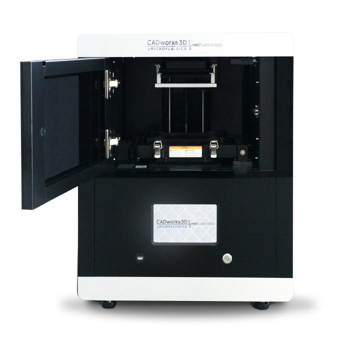
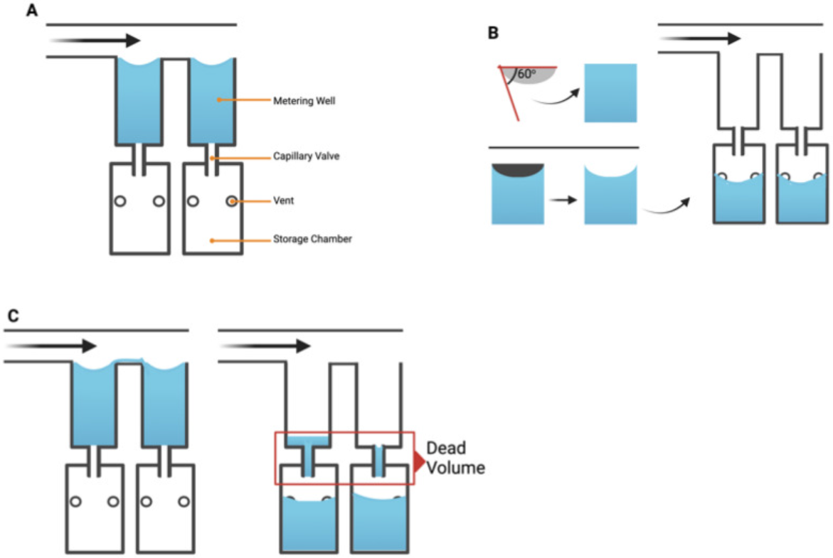
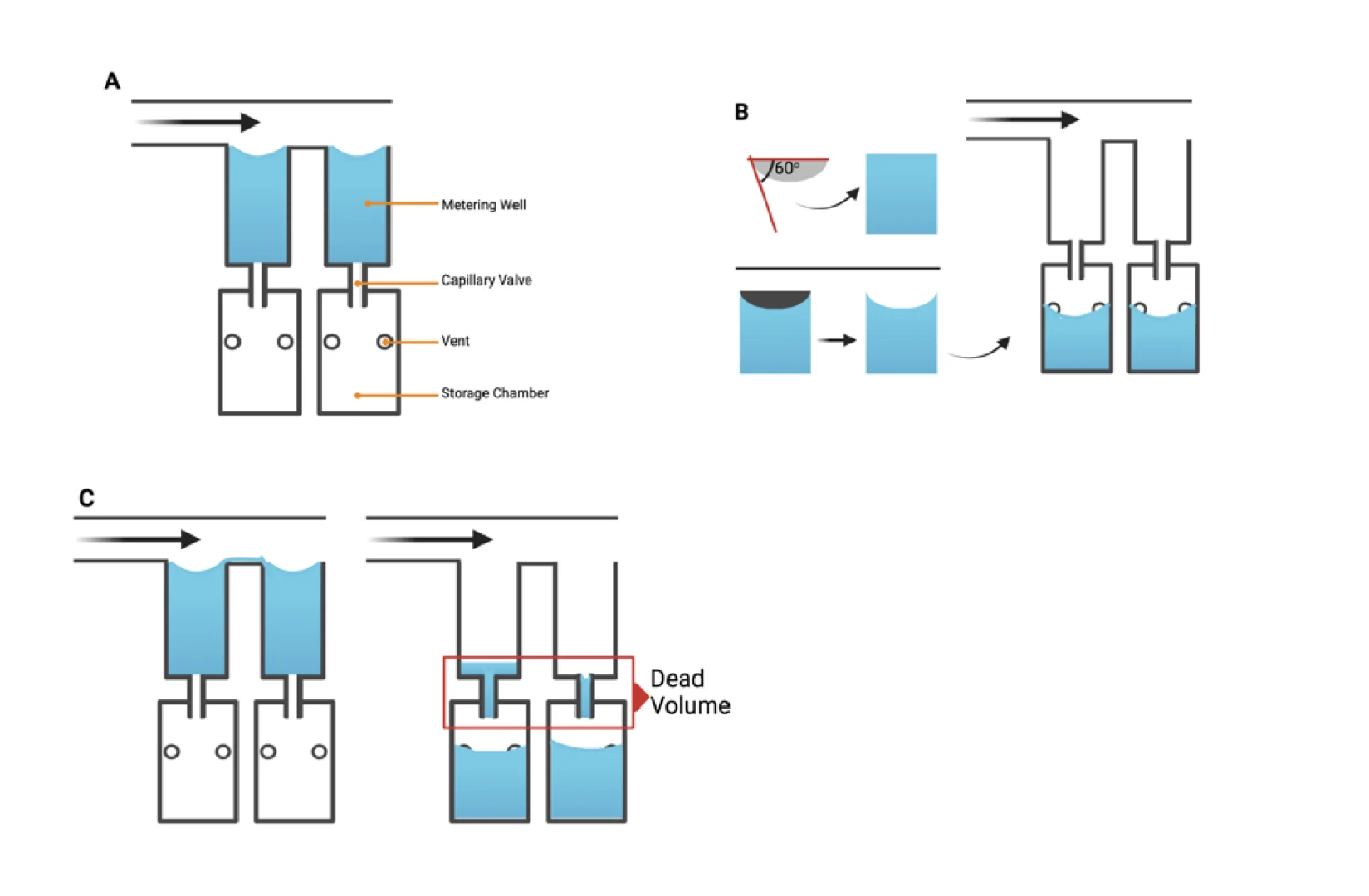
The chip was designed as a 16-well manifold for fluid and particle metering devices in which the metering chambers are separated from a lower storage chamber by a capillary valve (Figure 1A). Having both chambers was necessary to prevent one of the consequences of manifold systems, which is sequential filling. This would entail that each well will be filled to the brim before the next, thereby leaving no headspace to allow for further fluid manipulations such as mixing. The lower storage chambers were perforated at positions modeled to provide a convex meniscus at the approximate intended fill volume. To achieve this on a 3D plane, a 60° hemisphere mimicking the hydrophilic contact angle between the chip surface and the buffer was used to cut an extrusion of the 3D-model infill until the desired fill volume was achieved on the model (Figure 1B). During assembly, the perforations were plugged with polytetrafluoroethylene (PTFE) membranes such that wicking of the metered volume into the membranes triggered an increase in the chamber pressure, thereby preventing further emptying of the top metering chamber (Figure 1C). All 3D models were designed using SolidWorks (Dassault Systèmes) and printed using ProFluidics 285D digital light processing (DLP) 3D printer (CADworks3D). The design files are included as Supplementary File (SF1).

Figure 1. Minimal illustrations of the chip sub-units showing critical design elements. (A) Metering and storage chambers separated by a capillary valve (B) Illustration showing method used to determine the position of the venting holes in the bottom (storage) chamber (C) Once fluid in the storage chamber wicks through the venting holes to a PTFE filter, the pressure within the chamber increases above the Laplace pressure. this prevents further filling of the storage chamber.

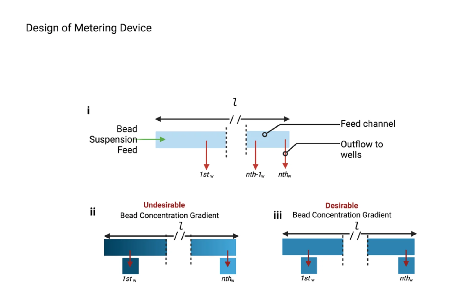
As illustrated in Figure 2, a consequence of the increased number of metering wells, n, is an increase in length of the flow path, l (Figure 2i), which consequently leads to a particle concentration gradient, in which the first well (Figure 2ii) contains a significantly greater concentration of suspended particles than the nth well due to bead settling. This challenge necessitates the need for a mechanism of counteracting or reducing the sedimentation of the beads to improve metering efficiency (Figure 2ii,iii).

Figure 2. (i) Illustration of the fluidic metering device showing the shared feed channel and the tributary wells (outflow channels). (ii) Illustration of undesirable (iii) desirable effect of bead settling as a result of sedimentation across the feed channel of length, l.

2.2. Hydrodynamic Interruption of Sedimentation

The interaction of particles of different sizes and shapes have been the subject of plenty of research, especially in environmental studies. However, there is a dearth of empirical demonstration of hydrodynamic interruption of particle sedimentation, especially in microfluidic systems. Here, the fabricated fluidic and particle-metering chips were used to demonstrate this phenomenon. The fabricated chips were connected to a syringe pump (Legato, KD Scientific, USA) via a modified Eppendorf tube, which held the bead suspension. For each experimental run, the syringe pump was programmed to run at a defined, arbitrarily chosen volumetric rate, Q = 1, 3.5, 5, and 10 mL/min until the feed channel was completely emptied. Each experimental condition was replicated (for Q = 1 mL/min, n = 2; for Q = 3.5, 5 and 10 mL/min, n = 3) to determine the reproducibility of the results. Before each run, the bead vial was vortexed to ensure uniform bead distribution, then connected to the metering device and pumped within 10 s, thereby preventing pre-settling of the beads. Visual data were collected using M50 Mark II mirrorless camera (Canon, USA) at 60 frames/s for computational image analysis via the algorithm described in the data acquisition and analysis section.


2.3. Induced Hindered Settling (i-HS)

The Richardson–Zaki modification of Stokes’ law [17,18] (Equation (1)) shows that at higher particle concentrations, the particle settling velocity decreases due to particle–particle interactions. This principle suggests that if we could increase the particle concentration in the buffer, we could delay or overcome particle settling. For biomedical applications, however, the particle concentrations are predetermined empirically for optimal performance and cost reasons and, as such, cannot be indefinitely increased to exploit the Richardson–Zaki principle. This principle could be exploited only if there was a way to transiently increase the particle concentration (or increase the turbidity of the particle-suspending solution) without introducing additional particles. This is the basis of the i-HS alternative.

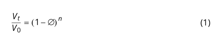
where 𝑉𝑡 = settling velocity in turbid fluid,
𝑉0 = settling velocity in clear fluid,
n = exponent of reduction in settling velocity,
⌀ = volume fraction of suspended particles in the fluid (turbidity)

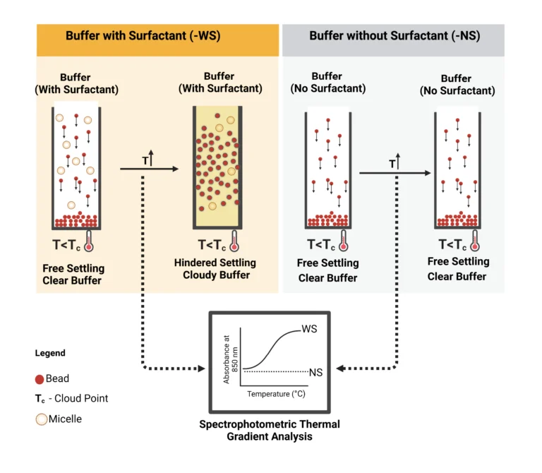
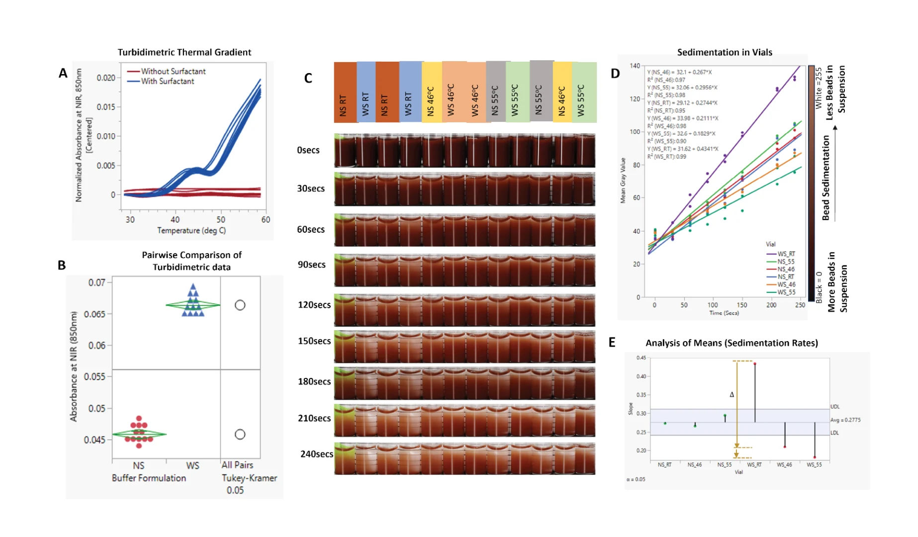
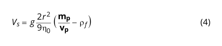
To ascertain the feasibility of the i-HS, the cloud point of the surfactant in the bead suspension buffer was exploited. Cloud point refers to a physical property (temperature) of non-ionic surfactants at which their dissolution in liquid reverses, leading to liquid–liquid phase separation. At this temperature, as illustrated in Figure 3, the surfactants form micelles, thereby increasing the turbidity (cloudiness) of the suspending solution. These micelles transiently act as particles, thereby allowing the empirical exploitation of the Richard–Zaki theory. As a preliminary analysis of this concept, the buffer was modified with and without ECOSURF EH-9 and designated with the prefixes -WS and -NS, respectively, and analysed via a spectrophotometric thermal gradient (STG) using BioTek Epoch 2 microplate spectrophotometer (Agilent, USA) in a 96-well plate. The choice of the non-ionic surfactant, ECOSURF EH-9, was informed by its biodegradability, among other functions such as wetting. Hypothetically, an increase in the turbidity of the -WS buffer relative to the turbidity of the -NS buffer would signal the feasibility of the concept.

Figure 3. Schematic representation of induced hindered settling and spectrophotometric thermal gradient analytical protocol.

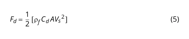
Subsequently, bead suspensions of the same concentration as in previous experiments were added to clear glass vials and grouped according to the experimental protocol This setup enabled the investigation of the effect of the surfactant cloud point on bead settling. Test temperatures that can be tolerated by downstream processes (50 ± 10 °C), and at which cloud point was induced were chosen from different temperature points on the STG data for further sedimentation analyses. Raw STG data are included as Supplemetary Data, SD1.


2.4. Data Acquisition and Analysis

Replicate (n = 12) turbidimetric measurements at different temperatures and data collection were achieved using a spectrophotometer at a near-infrared (NIR) wavelength of 850 nm. For bead settling experiments, heating of the glass vials for bead settling was performed using a Benchmark Multitherm shaker and cooling device. Visual data in the form of video recordings were collected for the assessment of bead settling and suspension homogeneity in the vials using M50 Mark II Mirrorless camera (Canon, USA) at 60 frames per second). Each test was run in duplicates.


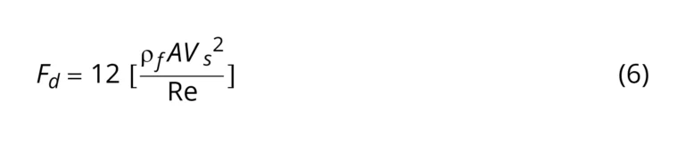
The collected videos were analysed using Python 3.6 computer vision library (OpenCV) following the algorithm shown in Figure 4. To determine the bead settling velocity in the vials, the intensity of the pixels within the region of interest (region covered by the bead suspension) was monitored throughout the video timeline. By monitoring the pixel intensity over time, the presence and later absence of beads within a pixel signals the settling of the beads. The sedimentation rate was determined as the rate of change of gray value (Equation (2)).
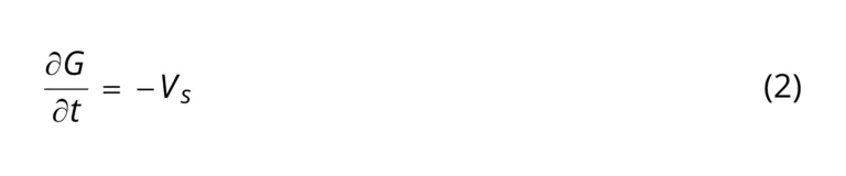
where 𝐺/𝑡 = rate of change of gray values over time, 𝑉s = sedimentation rate

Figure 4. Still and a video image processing algorithm for feature extraction and numerical data retrieval.

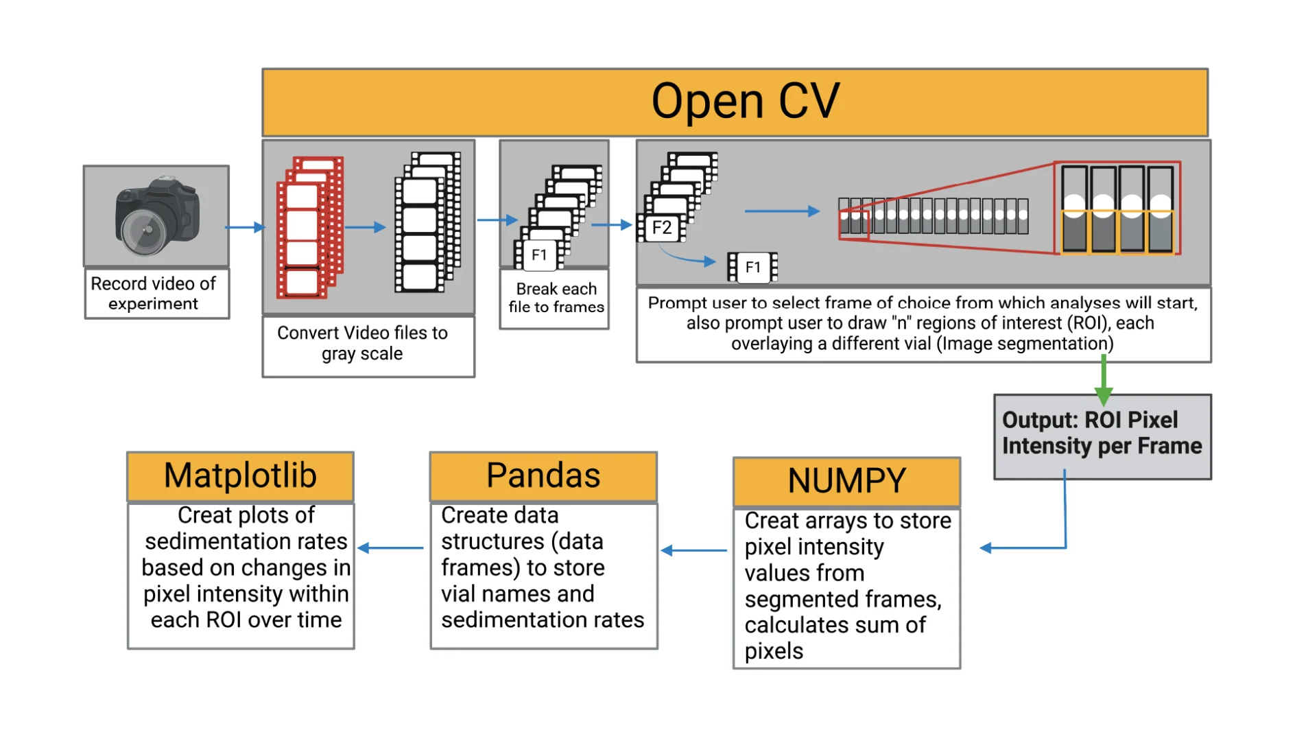
The pixel intensity (mean gray value) refers to the brightness of a pixel in an image. From the grayscale images, the intensity was measured on a scale of 0–255, where 0 represents black and 255 represents white. The mean gray values correspond to the concentration of the beads or the homogeneity of the bead suspension.

3. Results

3.1. Fabrication of Particle Metering Chip

To prevent premature emptying of the top metering wells, the dimensions of the feed channel were modeled using 2023 SolidWorks Flow Simulations software (Dassault Systèmes). The capillary stop valves were designed to have a Laplace pressure of 403 Pa, calculated using Equation (3).

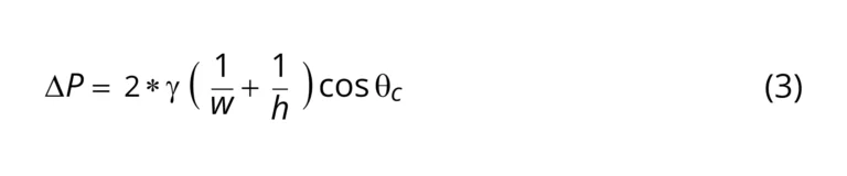
where 𝜃𝑐 = fluid contact angle = 2, w = valve width = 0.5 mm, h = valve height = 1.25 mm, 𝛾 = 𝛾water = surface tension = 0.072 N/m.

After printing, the geometric conformance of the 3D-printed capillary valves to the CAD model was determined using optical metrology (Keyence). This was determined to be 0.49 ± 0.02 mm (n = 10), thus conforming with the design parameters (Equation (3)).

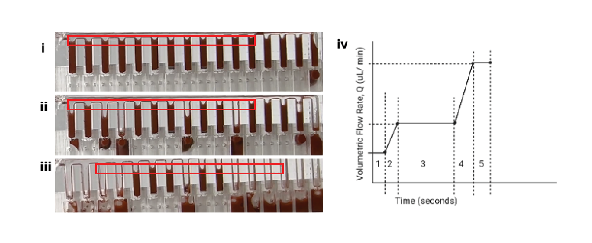
A major consequence of manifold splitting results from the interaction between the buffer, the shared walls between wells, the material surface properties, and the flow regime (Figure 5iii). This interaction led to an undesired siphon effect, whereby asynchronously emptied wells drew fluid from neighboring wells, leading to metering inefficiencies. This was resolved by reprogramming the flow regime to ensure synchronous emptying of the wells via an instantaneous increase in Laplace pressure (Figure 5iv).

Figure 5. (i–iii) shows the effect of asynchronous emptying of the metering wells. (iv) shows the pump ramp program: (2) Ramp from 0.1 mL/min to 1 mL/min in 5 s. (3) Hold at 1 mL/min for 72 s (72 s is the time required to completely empty the surrogate elution chamber per my setup + time to empty the feed well) (4) Ramp from 1 mL/min to 10 mL/min in 5 s (5 s–arbitrarily chosen—being careful to ensure the syringe pump could handle that ramp) (5) Hold at 10 mL/min for 6 s (10 mL/min for 6 s ensures 690 µL is pushed from the all metering wells while keeping the unit pressurized). The positive pressure is maintained momentarily to ensure all wells are emptied simultaneously.

3.2. Hydrodynamic Interruption of Sedimentation

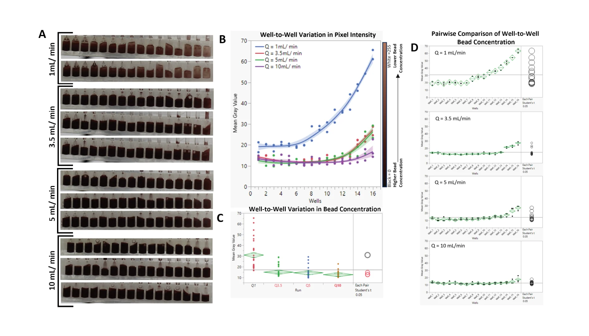
As shown in Figure 6A,B, at a volumetric flow rate of Q = 1 mL/min, much of the beads eluted early in the experimental run, forcing the mean gray value (MGV) of wells 1 through 7 to be significantly lower (higher bead concentration) than that of wells 8–16 (Figure 6D). Pairwise comparisons (Student’s t test, alpha = 0.05) of the MGVs of the 16 wells from Q = 1 mL/min to the other tested Qs revealed a significant difference between them, with p values < 0.0001 (Figure 6C). While increasing Q from 3.5 mL/min to 10 mL/min did not significantly affect the average concentration of the beads (p values: Q3.5 − Q10 = 0.107; Q5 − Q10 = 0.231; Q3.5 − Q5 = 0.675), analyses of the data from each flow rate showed improved bead distribution (Figure 6D). For Q = 3.5 mL, wells 14–16 had significantly lower bead concentrations; for Q = 5 mL/min, wells 15 and 16 had significantly lower bead concentrations; and for Q = 10 mL/min, only well 16 had a significantly lower bead concentration. Video recording of the analyses can be found in the Supplementary Folder, SD2.

Figure 6. (A). Cropped frames showing well-to-well variation in bead concentration per flow rate. (B). Distribution pattern of the suspended beads in response to changes in the volumetric flow rate. (C). Comparison of the effect of flow rate on the mean bead concentration. (D). Pairwise comparison of well-to-well bead concentrations.

3.3. Sedimentation Offset via Induced Hindered Settling

Phase separation in the particle suspension buffer was induced and confirmed via spectrophotometric analyses, which showed a temperature-driven increase in turbidity (Figure 7A). As this change is reversible [19], it offers a perfect solution for increasing the probability of particle–particle interactions and, consequently, hindering settling. Incubation of the WS buffer at 55 °C resulted in a ~45% increase in turbidity (Figure 7B).

Figure 7. (A). Spectrophotometric thermal gradient (STG) analysis of buffers with (-WS) and without (-NS) surfactants. (B). Pairwise comparison of STG results. (C). Timelapse images showing bead sedimentation in glass vials. (D). XY plots of different experimental conditions showing the temporal rate of change in pixel intensity. (E). Analysis of means (ANOM) of the sedimentation gradients (𝛼 = 0.05). Video data of the experimental setup is included in Supplementary Folder, SD3.

As shown in Figure 7C,D, this phenomenon translated to a reduction in bead settling velocity. In accordance with the theory of hindered settling, an increase in the bead suspension buffer temperature and, consequently, the cloud point of the surfactant reduced the sedimentation rate of the beads by 58% (Figure 7D,E). Continuous or controlled heating of the beads in a vial showed a similar result of improved particle metering. Notably, the presence of surfactants, while necessary for fluid flow, increases the bead settling velocity, as shown in Figure 7C–E—WS_RT (slope = 0.4341) vs. NS_RT (slope = 0.2744). As shown in Figure 7E, there was no significant difference in sedimentation rate between -NS buffer at room temperature and one heated to 46 °C (NS_46 °C vs. NS_RT); however, increasing the temperature of the -NS group to 55 °C led to an increase in the rate of sedimentation (NS_46—slope: 0.267, NS_55—slope: 0.296).

Apparatus Used

ProFluidics 285D

4. Discussion

4.1. Hydrodynamic Interruption of Particle Sedimentation

Particle sedimentation occurs because of the action of gravitational pull on the particles. The rate at which particles sediment, 𝑉𝑠, is influenced by factors such as particle volume and the density of the suspending fluid.

𝑉𝑠 = is Sedimentation velocity at infinite dilution, r = particle radius, 𝜂0 = viscosity of suspending fluid, 𝑚𝑝= mass of particle, 𝑣𝑝 = volume of particle, 𝜌𝑓 = density of suspending fluid, g = |g| = 9.8m/s2.

These, in turn, also influence the drag force, (𝐹𝑑), which in simple terms, the drag force refers to the resistance force exerted by a fluid to the downward motion of the particles.

where 𝐹𝑑 = drag force, V = particle velocity, A = particle area, C𝑑 = drag coefficient = 24/Re for spheres [20], therefore:

Substituting 𝑔 (2𝑟2 / 9𝜂0([𝑚𝑝 / 𝑣𝑝] 𝜌𝑓) for 𝑉𝑠 in Equation (5)

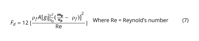
As shown in Equation (7), several factors contribute to the drag force exerted on the particles. Consider particles at a steady state, as illustrated in Figure 8, the particles sediment in response to the resultant of opposing forces, drag force, and gravity.

Figure 8. Working theory for hydrodynamic interruption of particle sedimentation. (A) At steady state, particles in suspension are acted on by two forces F_D (drag force) and F_g (gravitational pull) whose resultant is denoted by F_g’ and is determined by the magnitude of the counteracting forces. (B) Shows the resultant of forces acting on particles suspended in fluids in flow.

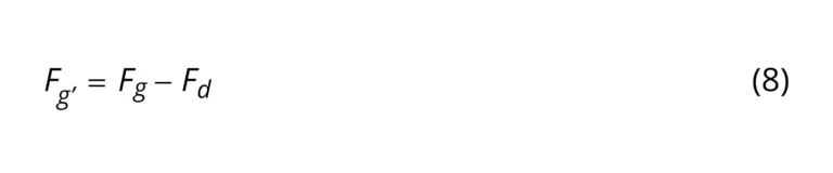
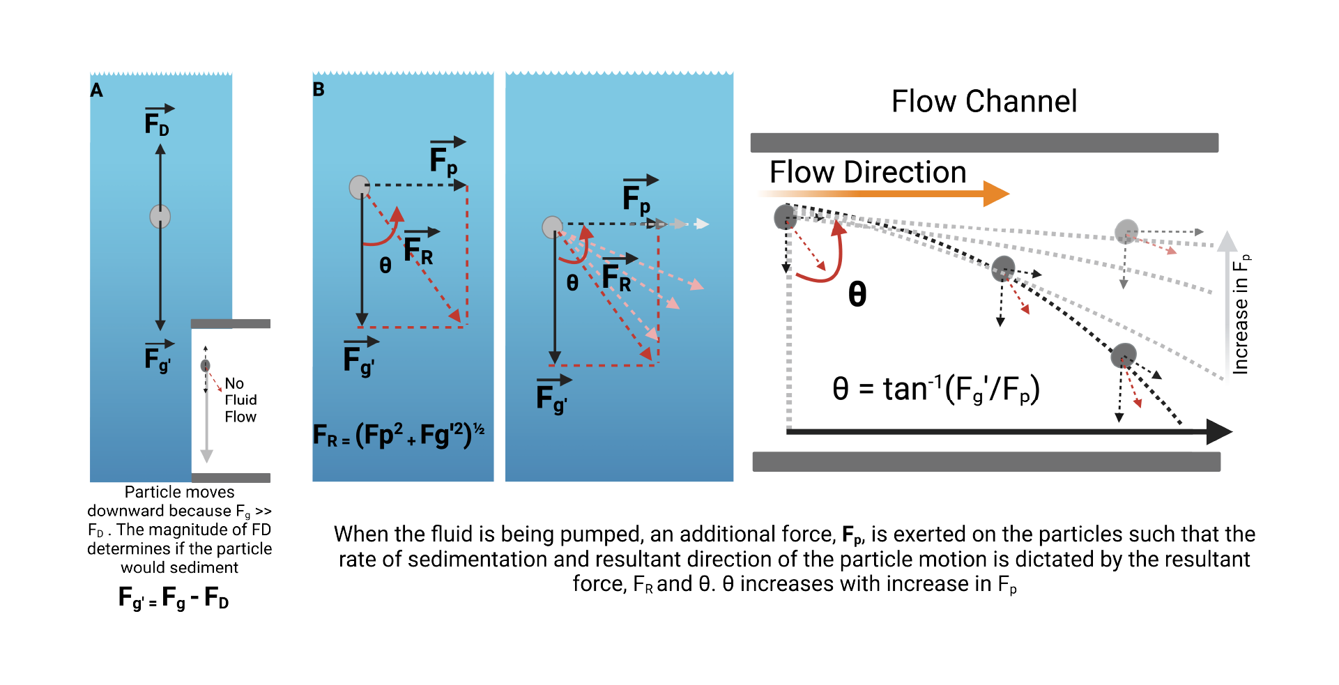
However, in a fluidic state, the rate and direction of sedimentation is largely determined by the magnitude of the force, 𝐹𝑝 applied to the particle due to pumping.


As the deviation of the particle from a straight downward sedimentation is given by:

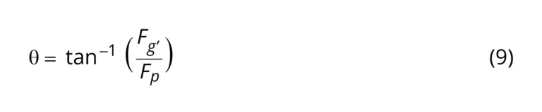
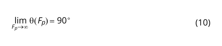
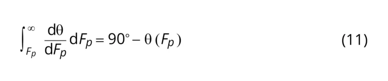
Theoretically, at constant |g’|, increasing 𝐹𝑝 would result in a concomitant increase in 𝜃 towards 90°.

Considering this theory, as 𝐹𝑝 = ma, where m=mass; and a = acceleration = Fluid Velocity / time,
𝐹𝑝 can be increased via the volumetric flow rate.


Empirical findings from the data above validate the working theory as stated in Equations (9)–(11); thus, as the acceleration of the beads in solution increase as a result of the increase in Q of the suspending fluid, gravitational pull on the particles is counteracted. The particles therefore remain homogenized in solution long enough to be evenly distributed. This method, although simplistic and easy to implement in most systems, may be impractical for shear-averse processes where high flow rates (deviation from laminar flow) could impact the structural integrity of the suspended particles. Additionally, as shown in Figure 6C, increasing Q beyond a certain threshold yields very minimal improvement, which may not justify the high volumetric flow rate requirement. These limitations, therefore, necessitate the need for a more shear-tolerant alternative that would not only alter the sedimentation trajectory, but also significantly reduce it.


4.2. Induced Hindered Settling

Although ECOSURF EH-9 has a cloud point of 64 °C at 10 wt% actives aqueous solution, the spectrophotometric thermal gradient data (Figure 7A) show that at 0.1 wt%, turbidimetric changes could be initiated at temperatures lower than the cloud point. This finding improves on the existing knowledge that heating solutions containing non-ionic surfactants to temperatures above the surfactant cloud point (Tc) could induce a phase change [21]. While the exact role of the salts in the proprietary buffer on the lower cloud point was not explored, data from [22] suggest that the cloud point of non-ionic surfactants could be lowered via the addition of salts. Figure 7A also shows a biphasic change in buffer turbidity relative to temperature increase. The primary reason for this biphasic relationship could not be determined from secondary data; however, a thermally-induced phase change due to surfactant cloud point could explain an increase in turbidity. This phase change results in the formation of surfactant micelles that interact with the particles, thereby conforming to the Richardson–Zaki theory. Although this phase change can also be induced chemically via the addition of ionic surfactant and electrolytes, for this application, micellar aggregation occurred because of thermally induced reduction in the hydration of oxyethylene oxygen in hydrophilic groups, which leads to micellar aggregation. This phenomenon has been widely adopted in environmental studies and in separation science as a form of cloud point extraction (CPE) [21,23,24,25,26]. While encouraging, most applications requiring microparticle manipulation may not be tolerant to heating. For such applications, the choice of surfactants with cloud points closer to tolerable temperatures or chemical tuning [22] of the surfactant cloud point may be ideal.

5. Conclusions

Various biomedical applications, especially in microfluidic systems, require microparticle handling [27]. The development of specialized devices for continuous mixing [28,29,30,31] or a complete switch to gel beads has been mostly adopted due to the challenge of bead settling. However, these factors increase the cost and complexity of the system. This paper presents two simplistic solutions, hydrodynamic and i-HS solutions. Both solutions exploit rudimentary components in biomedical platforms, thereby not adding to the cost. While they can be applied independently, they can also be combined to achieve a uniform distribution of particles of various sizes or to lower their settling velocity for fluidic applications. This was successfully applied in particle metering and distribution manifold. A limitation of both systems is the requirement for an initial homogenization step and continued heating for the i-HS (optional). Moreso, the thermal induction of hindered settling as demonstrated in this research may not be ideal for most biomedical systems. However, thermal i-HS may not be necessary, considering the possibility of non-thermal cloud point tuning [22]. These principles can be adopted in particle-laden flows involving the need for mechanistic encapsulation of microparticles. More so, to the best of our knowledge, there are no published studies that explore the integration of mechanical agitation and multi-well particle metering to set a comparative baseline. This study establishes such a baseline. Further, continuous mechanical agitation of particle suspensions upstream does not influence particle behaviours downstream where convective flows are negligible; as such, regardless of mechanical mixing in bulk solution, additional measures are required to forestall undesirable sedimentation of particles.

Supplementary Materials

References

  1. Iwai, K.; Sochol, D.R.; Lin, L. A bead-in-droplet solution exchange system via continuous flow microfluidic railing. In Proceedings of the 2013 IEEE 26th International Conference on Micro Electro Mechanical Systems (MEMS), Taipei, Taiwan, 20–24 January 2013; pp. 1203–1206. [Google Scholar]
  2. Kim, H.; Choi, I.H.; Lee, S.; Won, D.J.; Oh, Y.S.; Kwon, D.; Sung, H.J.; Jeon, S.; Kim, J. Deterministic bead-in-droplet ejection utilizing an integrated plug-in bead dispenser for single bead-based applications. Sci. Rep. 2017, 7, 1–9. [Google Scholar] [CrossRef]
  3. Price, A.K.; Macconnell, A.B.; Paegel, B.M. Microfluidic bead suspension hopper. Anal. Chem. 2014, 86, 5039–5044. [Google Scholar] [CrossRef] [PubMed]
  4. Myers, K.K.; Herich, J.P.; Chavez, J.E.; Berkey, K.G.; Loi, A.J.; Cleveland, P.H. A Novel Method to Gently Mix and Uniformly Suspend Particulates for Automated Assays. SLAS Technol. 2021, 26, 498–509. [Google Scholar] [CrossRef]
  5. Wang, C.H.; Lien, K.Y.; Wu, J.J.; Lee, G.B. A magnetic bead-based assay for the rapid detection of methicillin-resistant Staphylococcus aureus by using a microfluidic system with integrated loop-mediated isothermal amplification. Lab A Chip 2011, 11, 1521–1531. [Google Scholar] [CrossRef]
  6. Anyaduba, T.D.; Otoo, J.A.; Schlappi, T.S. Picoliter Droplet Generation and Dense Bead-in-Droplet Encapsulation via Microfluidic Devices Fabricated via 3D Printed Molds. Micromachines 2022, 13, 1946. [Google Scholar] [CrossRef] [PubMed]
  7. Sassolas, A.; Hayat, A.; Marty, J.L. Immobilization of enzymes on magnetic beads through affinity interactions. Methods Mol. Biol. 2013, 1051, 139–148. [Google Scholar] [CrossRef]
  8. Vashist, S.K.; Luong, J.H. Antibody Immobilization and Surface Functionalization Chemistries for Immunodiagnostics; Elsevier: Amsterdam, The Netherlands, 2018; pp. 19–46. [Google Scholar] [CrossRef]
  9. Poles, M.; Meggiolaro, A.; Cremaschini, S.; Marinello, F.; Filippi, D.; Pierno, M.; Mistura, G.; Ferraro, D. Shaking Device for Homogeneous Dispersion of Magnetic Beads in Droplet Microfluidics. Sensors 2023, 23, 5399. [Google Scholar] [CrossRef] [PubMed]
  10. Banerjee, U.; Jain, S.K.; Sen, A.K. Particle encapsulation in aqueous ferrofluid drops and sorting of particle-encapsulating drops from empty drops using a magnetic field. Soft Matter 2021, 17, 6020–6028. [Google Scholar] [CrossRef]
  11. Anyaduba, T. Primer Payload System for Higher-Order Multiplex LAMP: Design and Development of Unit Processes. Ph.D. Dissertation, Keck Graduate Institute, Claremont, CA, USA, 2021. [Google Scholar]
  12. Shintaku, H.; Kuwabara, T.; Kawano, S.; Suzuki, T.; Kanno, I.; Kotera, H. Micro cell encapsulation and its hydrogel-beads production using microfluidic device. Microsyst. Technol. 2007, 13, 951–958. [Google Scholar] [CrossRef]
  13. Klein, A.M.; Mazutis, L.; Akartuna, I.; Tallapragada, N.; Veres, A.; Li, V.; Peshkin, L.; Weitz, D.A.; Kirschner, M.W. Droplet barcoding for single-cell transcriptomics applied to embryonic stem cells. Cell 2015, 161, 1187–1201. [Google Scholar] [CrossRef]
  14. Zilionis, R.; Nainys, J.; Veres, A.; Savova, V.; Zemmour, D.; Klein, A.M.; Mazutis, L. Single-cell barcoding and sequencing using droplet microfluidics. Nat. Protoc. 2017, 12, 44–73. [Google Scholar] [CrossRef]
  15. Clark, I.C.; Abate, A.R. Microfluidic bead encapsulation above 20 kHz with triggered drop formation. Lab A Chip 2018, 18, 3598–3605. [Google Scholar] [CrossRef] [PubMed]
  16. Ekanayake, N.I.; Berry, J.D.; Stickland, A.D.; Dunstan, D.E.; Muir, I.L.; Dower, S.K.; Harvie, D.J. Lift and drag forces acting on a particle moving with zero slip in a linear shear flow near a wall. J. Fluid Mech. 2020, 904, A6. [Google Scholar] [CrossRef]
  17. Riuxardson, J.F.; Zaki, W.N. The sedimentation of a suspension of uniform spheres under conditions of viscous flow. Chem. Eng. Sci. 1954, 3, 65–73. [Google Scholar] [CrossRef]
  18. Zhu, Z.; Wang, H.; Peng, D.; Dou, J. Modelling the hindered settling velocity of a falling particle in a particle-fluid mixture by the Tsallis entropy theory. Entropy 2019, 21, 55. [Google Scholar] [CrossRef] [PubMed]
  19. Ghaedi, M.; Shokrollahi, A.; Mehrnoosh, R.; Hossaini, O.; Soylak, M. Combination of cloud point extraction and flame atomic absorption spectrometry for preconcentration and determination of trace iron in environmental and biological samples. Cent. Eur. J. Chem. 2008, 6, 488–496. [Google Scholar] [CrossRef]
  20. Mariusz, R.; Ewelina, L. Modeling of the sedimentation process of monodisperse suspension. Int. J. Comput. Methods Exp. Meas. 2022, 10, 50–61. [Google Scholar] [CrossRef]
  21. Miyake, M.; Yamashita, Y. Molecular Structure and Phase Behavior of Surfactants. In Cosmetic Science and Technology: Theoretical Principles and Applications; Elsevier: Amsterdam, The Netherlands, 2017; pp. 389–414. [Google Scholar] [CrossRef]
  22. Cloud Point of Non-Ionic Surfactants—METTLER TOLEDO. Available online: https://www.mt.com/gb/en/home/library/applications/lab-analytical-instruments/cloud-point-non-ionic-surfactant.html#:~:text=Importance%20of%20the%20Cloud%20Point,non%2Dionic%20surfactants%20in%20water. (accessed on 19 August 2024).
  23. Nazar, M.F.; Shah, S.S.; Eastoe, J.; Khan, A.M.; Shah, A. Separation and recycling of nanoparticles using cloud point extraction with non-ionic surfactant mixtures. J. Colloid Interface Sci. 2011, 363, 490–496. [Google Scholar] [CrossRef]
  24. Duester, L.; Fabricius, A.L.; Jakobtorweihen, S.; Philippe, A.; Weigl, F.; Wimmer, A.; Schuster, M.; Nazar, M.F. Can cloud point-based enrichment, preservation, and detection methods help to bridge gaps in aquatic nanometrology? Anal. Bioanal. Chem. 2016, 408, 7551–7557. [Google Scholar] [CrossRef]
  25. Na, G.C.; Yuan, B.O.; Stevens, H.J.; Weekley, B.S.; Rajagopalan, N. Cloud point of nonionic surfactants: Modulation with pharmaceutical excipients. Pharm. Res. 1999, 16, 562–568. [Google Scholar] [CrossRef]
  26. Al-Saadi, M.R.; Al-Garawi, Z.S.; Thani, M.Z. Promising technique, cloud point extraction: Technology & applications. J. Phys. Conf. Ser. 2021, 1853, 012064. [Google Scholar]
  27. Cremaschini, S.; Torriero, N.; Maceri, C.; Poles, M.; Cleve, S.; Crestani, B.; Meggiolaro, A.; Pierno, M.; Mistura, G.; Brun, P.; et al. Magnetic Stirring Device for Limiting the Sedimentation of Cells inside Microfluidic Devices. Sensors 2024, 24, 5014. [Google Scholar] [CrossRef] [PubMed]
  28. Burgoyne, F. Preventing Suspension Settling during Injection—Chips and Tips. Available online: https://blogs.rsc.org/chipsandtips/2007/08/21/preventing-suspension-settling-during-injection/?doing_wp_cron=1724225330.9217240810394287109375 (accessed on 19 August 2024).
  29. Chong, W.H.; Chin, L.K.; Tan, R.L.S.; Wang, H.; Liu, A.Q.; Chen, H. Stirring in Suspension: Nanometer-Sized Magnetic Stir Bars. Angew. Chem. Int. Ed. 2013, 52, 8570–8573. [Google Scholar] [CrossRef]
  30. Suk Ryu, K.; Shaikh, K.; Goluch, E.; Fan, Z.; Liu, C. Micro magnetic stir-bar mixer integrated with parylene microfluidic channels. Lab A Chip 2004, 4, 608–613. [Google Scholar] [CrossRef]
  31. Lane, S.I.R.; Butement, J.; Harrington, J.; Underwood, T.; Shrimpton, J.; West, J. Perpetual sedimentation for the continuous delivery of particulate suspensions. Lab A Chip 2019, 19, 3771–3775. [Google Scholar] [CrossRef] [PubMed]

Microfabricated dynamic brain organoid cocultures to assess the effects of surface geometry on assembloid formation

Academic Article

Microfabricated dynamic brain organoid cocultures to assess the effects of surface geometry on assembloid formation

Camille Cassel de Camps, Sabra Rostami, Vanessa Xu, Chen Li, Paula Lépine, Thomas M. Durcan and Christopher Moraes

Organoids have emerged as valuable tools for the study of development and disease. Assembloids are formed by integrating multiple organoid types to create more complex models. However, the process by which organoids integrate to form assembloids remains unclear and may play an important role in the resulting organoid structure. Here, a microfluidic platform is developed that allows separate culture of distinct organoid types and provides the capacity to partially control the geometry of the resulting organoid surfaces. Removal of a microfabricated barrier then allows the shaped and positioned organoids to interact and form an assembloid. When midbrain and unguided brain organoids were allowed to assemble with a defined spacing between them, axonal projections from midbrain organoids and cell migration out of unguided organoids were observed and quantitatively measured as the two types of organoids fused together. Axonal projection directions were statistically biased toward other midbrain organoids, and unguided organoid surface geometry was found to affect cell invasion. This platform provides a tool to observe cellular interactions between organoid surfaces that are spaced apart in a controlled manner, and may ultimately have value in exploring neuronal migration, axon targeting, and assembloid formation mechanisms.

Keywords: Assembloid; brain organoid; co‐culture; organ‐on‐a‐chip.

We kindly thank the researchers at McGrill University for this collaboration and for sharing the results obtained with our CADworks3D system.​

1. Introduction

Organoids have gained popularity as experimental models for developmental and disease studies.[1-11] Grown from stem cells, these 3D tissue-engineered cultures can differentiate toward diverse lineages that capture the complexity of in vivo tissues.[1-9] Multiple organoid types can also be assembled to interact, fuse, and mature[12-14] and these “assembloids” can hence capture some of the additional cellular diversity and architectural complexity of multi-component organ systems, compared to single-type organoids.[12, 13, 15, 16] In the developing brain, for example, complex circuits are established by neuronal projection and migration to create both local and long-distance connections.[13, 17-19] Regionalized organoids can hence be assembled to create in vitro models of the circuits that run throughout the brain. For example, functional synaptic connections can form between cortical and striatal organoids, specific neurons can migrate from ventral to dorsal forebrain organoids,[20, 21] and muscle contraction can be stimulated by brain organoid activity.[22] Assembloids can hence be powerful in vitro models for a wide variety of neurodevelopmental disease processes.[20, 21]

Tissue geometry is now well-established to influence fundamental cellular processes, such as proliferation, differentiation, branching, and invasion.[23-30] Driven by endogenous mechanical cellular stresses that spontaneously arise in three-dimensional tissues,[24, 25, 31] these cellular phenotypes drive feedback loops that govern tissue organization, specification, and maturation.[23, 26, 32] While previous studies have demonstrated that geometric confinement and associated mechanical stresses drive the organization of developing neural structures,[33, 34] whether these geometric features play a role in neural organoid development and assembloid formation remains an open question. Such experiments would require the technical capacity to simultaneously impose a specific geometry on independently cultured organoids, and control their relative positions before allowing them to interact. Moreover, such experiments would require long-term culture in biologically permissive and optically addressable formats. Given the intrinsic challenges associated with precisely manipulating soft living matter, technical innovations are required to better understand assembloid formation.

Recent developments in organoid culture models suggest a path to achieve these goals. Park et al. recently developed a microfabricated culture approach in which oxygen-permeable silicone inserts are used to restrict the size and shape of intestinal organoids as they grow into a hydrogel matrix.[35] This approach was successfully used to allow stem cell proliferation and maturation, while controlling the global geometry of mature intestinal organoids, such that diffusive transport of oxygen, nutrients, and waste was sufficient to prevent the formation of a necrotic core that commonly arises in large, dense tissues.[35] Although very promising, this strategy has yet to be demonstrated for other types of organoids. Inspired by this approach, here we develop a strategy to separately culture distinct brain organoid types in adjacent compartments, while shaping the surface geometry of the tissues; and explore this concept using two types of brain organoids. After establishing mature organoids, an insert separating the organoid compartments can be manually removed and replaced with a thin layer of extracellular matrix, allowing the precisely positioned organoids to begin forming an assembloid (Figure 1). To prove this concept, here we use various channel geometries to shape unguided and midbrain organoids. We demonstrate simultaneous axonal projections emanating from the midbrain organoids, and surface geometry-specific cell migration from unguided organoids. We hence propose that this technical innovation allows systematic investigation of the role of interacting surface geometries in assembloid formation.

Figure 1. Schematic of device for coculture and assembloid formation. Two different types of organoids are loaded into separate channels and fed by separate media reservoirs. The geometry of the wall separating the channels shapes the organoids as they grow. When mature, the separating wall can be physically removed, allowing the organoids to interact and eventually fuse, while observing their interactions throughout culture.

2. Methods

Unless otherwise stated, all cell culture materials and supplies were purchased from Fisher Scientific (Ottawa, ON) and chemicals were from Sigma-Aldrich (Oakville, ON). The use of induced pluripotent stem cells (iPSCs) in this research was approved by the McGill University Health Centre Research Ethics Board (DURCAN_IPSC/2019-5374).


2.1. Device fabrication process

Molds were designed in Fusion 360 (AutoDesk), and printed on a ProFluidics 285D 3D resin printer using Master Mold Resin (CADworks3D) with a layer thickness of 50 µm. After washing with isopropanol, mold pieces were cured in a 36 W ultraviolet (UV) chamber overnight. Molds were designed for assembly into chambers with patterned features on both the base and lid (Figure 2A). Polydimethylsiloxane (PDMS) prepolymer and curing agent were mixed at a ratio of 10:1 w/w, poured into the chamber, and degassed under vacuum. The molded lid was then lowered slowly from one side to avoid trapping air bubbles in the chamber. The lid was then pressed down to displace excess PDMS. Tongue-and-groove convex/concave features in the chamber base and lid contained the PDMS prepolymer after chamber assembly. PDMS was cured overnight in an oven at 40°C to minimize shrinkage[36] and de-molded using 70% ethanol to help release the devices from the 3D printed resin.

Figure 2. Functional, separate channels and reservoirs. (A) Base and insert parts of displacement mold for casting devices for single cell culture. (B) Replica molded PDMS devices, shown with channels filled with dye, left, and reservoirs filled, middle and right. (C) T47D cells were stained with CellTracker Red or Green, and then loaded into channels with Matrigel. After 3 days of culture, cells remain separated in their respective channels. (D) T47D cells were loaded with Matrigel into both channels of a device, with cells in one channel dyed once inside the channel by adding CellTracker Green to that media reservoir. (E) iPSCs were loaded into channels with Matrigel, and cultured with midbrain organoid media. Live/dead staining shows high viability after 7 days in culture.

Apparatus Used

Master Mold for PDMS

ProFluidics 285D

Apparatus Used

Master Mold for PDMS

ProFluidics 285D

2.2. Device preparation for organoid culture

Base devices were coated with dopamine to improve adhesion to Matrigel.[37] Briefly, dopamine hydrochloride was dissolved in 10 mM Tris buffer (pH 8.5; 2 mg mL−1), pipetted into the devices, and incubated overnight at room temperature. After treatment, devices were rinsed in reverse osmosis water, and dried with a stream of dry compressed air. To facilitate release from the devices and reduce adhesion to tissue cultures, the removable inserts were passivated with Pluronic® F-68 (5% in water) overnight at room temperature.[38, 39] Treated devices were rinsed in water, and dried with compressed air. All components were sterilized for 20 min in a 36 W UV chamber before assembly. Devices were assembled on a coverslip, which formed the bottom of the media reservoirs and allowed the device to be easily manipulated as a unit. For experiments without a removable insert, glass coverslips were used as the base surface, after functionalization with dopamine. Assembled devices were sterilized by UV for 45 min.

2.3. Cell culture

The AIW002-2 iPSC line (male) was used to generate unguided (previously referred to as “cerebral” organoids), and the TD22 iPSC line (male) was used to generate midbrain organoids, following established and characterized protocols[40, 41] with some previously-described modifications.[42] Both lines were obtained from The Neuro’s C-BIG repository and had undergone multistep quality control.[43] T47D human breast cancer cells (ATCC HTB-133) were used for preliminary validation experiments with the microfluidic device.

All cell cultures were maintained at 37°C with 5% CO2. T47D cells were cultured in Dulbecco’s Modified Eagle Medium with 10% fetal bovine serum and 1% antibiotic–antimycotic (complete DMEM). Media was changed every 3–4 days, and cells were passaged using 0.25% trypsin–EDTA at 80% confluence in a 1:5 dilution. The iPSC lines TD22 and AIW002-02 were maintained on Matrigel-coated plates in mTeSR1 complete kit media (Basal medium with supplement; STEMCELL Technologies, Cat No. 85850) with daily media changes. iPSC plated petri dishes were checked every day for spontaneous differentiation using a brightfield microscope. In cases where cells with morphologies different from iPSC colonies were detected, locations were marked and then in the BSC, cells on the marked locations were scraped off using a P200 pipette tip. Then, the media was collected, and the plate was washed with DMEM-F12 media supplemented with 1% antibiotic-antimycotic to ensure the removal of the scraped cells from the culture. iPSC cells were passaged with Gentle Cell Dissociation Reagent (StemCell Technologies) at 70% confluence. A ratio of 1:10 was maintained throughout all passages in which the colony pellet was broken down in such a way that each fragment contained between 10 and 15 cells. The homogeneity of the colony sizes in the sub-culture was assessed the next day by imaging with a brightfield microscope. At this step, colonies that were either too large or too small were scraped off and removed from the culture using the same method mentioned for removal of spontaneous differentiation.

2.4. Organoid culture

When iPSC cultures reached 70% confluence, cells were detached with Accutase (Gibco), resuspended in the appropriate media, seeded at 10,000 cells per well in 96-well round-bottom ultralow attachment plates (Corning Costar), and centrifuged for 10 min at 1200 rpm to aggregate the cells. Organoids were seeded so that they would be ready for Matrigel embedding simultaneously (Day 7 for midbrain, and Day 12 for unguided).


Media was changed every other day according to published protocols.[40, 41] For unguided organoids: human embryonic stem cell (hES) media (low basic fibroblast growth factor (bFGF), with ROCK inhibitor) was used on Day 0 (consisting of 400 mL DMEM-F12 + Glutamax, 100 mL Knockout Serum Replacement, 15 mL hESC-quality FBS (Gibco), 5 mL MEM- non-essential amino acids, 3.5 µL 2-mercaptoethanol, bFGF at 4 ng mL−1 final concentration, and ROCK inhibitor at 50 µM final concentration); hES media (low bFGF, no ROCK inhibitor) on Day 2; hES media (no bFGF, no ROCK inhibitor) on Day 4; neural induction media on Day 7 and 9 (consisting of DMEM-F12 + Glutamax, 1% N2 supplement, 1% MEM-non-essential amino acids (MEM-NEAA), and heparin at 1 µg mL−1 final concentration); cerebral organoid differentiation media without vitamin A on Day 12 and 14 (consisting of 125 mL DMEM-F12 + Glutamax, 125 mL Neurobasal, 1.25 mL N2 supplement, 62.5 µL insulin, 1.25 mL MEM-NEAA, 2.5 mL penicillin-streptomycin, 1.75 µL of 1/10 2-mercaptoethanol dilution in neurobasal, and 2.5 mL B27 supplement without vitamin A); cerebral organoid differentiation media with vitamin A on Day 16 onwards (made using B27 supplement with vitamin A).


For midbrain organoids: neuronal induction media was used on Day 0 (consisting of 25 mL DMEM-F12 + Glutamax + 1% antibiotic-antimycotic, 25 mL neurobasal, 500 µL N2 supplement, 1 mL B27 without vitamin A, 500 mL MEM-NEAA, 1.75 µL of 1/10 2-mercaptoethanol dilution in neurobasal, heparin at 1 µg mL−1 final concentration, SB431542 at 10 µM final concentration, noggin at 200 ng mL−1 final concentration, CHIR99021 at 0.8 µM final concentration, and ROCK inhibitor at 10 µM final concentration); neuronal induction media without ROCK inhibitor was used on Day 2; midbrain patterning media was used on Day 4 (consisting of neuronal induction media without ROCK inhibitor with the addition of Sonic Hedgehog (SHH) at 100 ng mL−1 final concentration, and Fibroblast Growth Factor 8 (FGF8) at 100 ng mL−1 final concentration); tissue induction media was used on Day 7 (consisting of 50 mL neurobasal, 500 µL N2 supplement, 1 mL B27 without vitamin A, 500 mL MEM-NEAA, 1.75 µL of 1/10 2-mercaptoethanol dilution in neurobasal, 12.5 µL insulin, laminin at 200 ng mL−1 final concentration, SHH at 100 ng mL−1 final concentration, FGF8 at 100 ng mL−1 final concentration, and 50 µL penicillin-streptomycin); final differentiation media was used on Day 8 onwards (consisting of 50 mL neurobasal, 500 µL N2 supplement, 1 mL B27 without vitamin A, 500 mL MEM-NEAA, 1.75 µL of 1/10 2-mercaptoethanol dilution in neurobasal, brain-derived neurotrophic factor (BDNF) at 10 ng mL−1 final concentration, glial cell line-derived neurotrophic factor (GDNF) at 10 ng mL−1 final concentration, ascorbic acid at 100 µM final concentration, db-cAMP at 125 µM final concentration, and 50 µL penicillin-streptomycin).


2.5. Device loading

Cell cultures were either loaded as single cells or as pre-formed organoids into the devices. Single cell cultures were obtained by trypsinization (T-47D, breast cancer line) or detachment (TD22 iPSCs, using Accutase as previously described[42]) and resuspended in undiluted Matrigel (Corning 356230) at concentrations of 8 × 10⁶ cells mL−1 for T-47D, or 1 × 10⁶, 3 × 10⁶, or 1 × 10⁷ cells mL−1 for iPSCs. All pipetting steps were performed with chilled pipette tips to prevent premature polymerization of the Matrigel. To load the organoids into the devices, they were pipetted directly into the loading ports in media with cut P200 pipette tips on Day 12 or 13 after seeding cerebral organoids, and on Day 7 or 8 for midbrain organoids. Once in the chamber, they were too big to pass through the channel restriction. Media was aspirated, leaving the organoids in the device, and replaced with undiluted Matrigel. All devices were incubated for 20 min at 37°C to polymerize the Matrigel. The appropriate media was added after polymerization, and replaced every 2 days.[40]


2.6. Insert removal

Once the organoids had grown and adopted the shapes defined by the compartment dimensions, the inserts separating the compartments were removed. One pair of tweezers was used to hold the base device down, while another was used to slowly pull the insert away. Media was gently aspirated from between the organoids, and replaced with Matrigel to fill in the space. Devices were left at room temperature for 5 min to allow the newly added liquid Matrigel to seep into the existing Matrigel, and then incubated for 20 min at 37°C. Final differentiation medium from the midbrain protocol,[40] with the addition of insulin at a concentration of 0.25 µL mL−1, was added to the well for this stage of combined culture. This media formulation was selected based on consultation and comparison of existing organoid and assembloid protocols and the function of each component,[21, 41, 44] and would need to be adjusted if other types of organoids were grown in the coculture device.


2.7. Tissue staining

Live CellTracker Green or Red were loaded into cells at 20 µM in media overnight at 37°C. Live/dead viability assays were performed with calcein AM and ethidium homodimer-1 (Life Technologies), diluted in media to 4 µM each and incubated with devices for 30 min at 37°C.


For immunostaining, Matrigel was first dissolved using Cell Recovery Solution (Corning; at 4°C for 20 min, twice). Devices were washed twice with phosphate buffered saline (PBS), fixed in 4% paraformaldehyde for 1 h at room temperature, and washed three times for 15 min each with PBS before storage at 4°C until staining. Whole mount staining was performed on organoids directly in the devices, using standard protocols.[42] Briefly, organoids were incubated in blocking buffer (0.5% Triton X-100 + 5% donkey serum in PBS) for 5 h at room temperature, then with primary antibodies diluted in blocking buffer overnight at 4°C. Organoids were then washed with PBS, three times for 15 min each, and then incubated with secondary antibodies and Hoechst diluted in blocking buffer overnight at 4°C. Organoids were washed again as before. Antibodies and stains were used as follows: anti-tyrosine hydroxylase (TH) at 1:200 (rabbit polyclonal, Pel Freez P40101-150), anti-β-tubulin III (Tuj1) at 1:300 (chicken polyclonal, Millipore Sigma AB9354), anti-tau-1 clone PC1C6 at 1:200 (mouse monoclonal, Millipore Sigma MAB3420), anti-glial fibrillary acidic protein (GFAP) at 1:250 (rabbit polyclonal, Millipore Sigma AB5804), anti-microtubule-associated protein 2 (MAP2) at 1:400 (chicken polyclonal, EnCor Biotechnology CPCA-MAP2), goat anti-chicken IgY H&L (DyLight® 488) at 1:500 (Abcam ab96947), donkey anti-rabbit IgG H&L (DyLight® 488) at 1:500 (Abcam ab96891), donkey anti-mouse IgG H&L (DyLight® 594) at 1:500 (Abcam ab96877), donkey anti-Rabbit IgG (H+L) Alexa Fluor™ 594 at 1:500 (Invitrogen A-21207), and Hoescht 33342 at 1:5000 (Invitrogen H3570). Immunostains were performed with a negative control (staining without primary antibody) to confirm that under these imaging conditions, any detected signals were not the result of non-specific binding or autofluorescence.


2.8. Microscopy and image analysis

Devices were imaged using an EVOS transmitted light microscope (XL Core) or an EVOS M7000 fluorescent Imaging System. Images were processed and analyzed in Fiji (NIH).[45] Pairwise stitching was performed using the Stitching plugin[46] when needed. Axonal projections were measured from the organoid surface to projection tip to obtain their length and angle. Cell migration distances were measured from the organoid surface to the edge of the migrating cell front, 2–3 days after removal of the separating wall.


2.9. Statistical analysis

Analyses were performed in R statistical software.[47] All data was confirmed to be normally distributed, with equal variances. The measurements of axonal projection lengths toward nearby organoids were normalized by lengths not directed towards a nearby organoid within samples, and then a two-sample, two-tailed t-test was used to compare between those axons that were directed towards midbrain organoids against those directed toward unguided organoids. The measurements of axonal projection angle for each organoid were used to calculate kurtosis, after centering distributions around the angle defined as toward the nearby organoid; one-sample t-tests were used to compare against random chance (i.e., uniform distribution, kurtosis of 1.8), and a two-sample, two-tailed t-test was used to compare between groups. One-way ANOVA was performed with Tukey post hoc comparisons for measurements of cell migration distance. All analyses for significance were carried out with α = 0.05.

3. Results

3.1. Device design for separated adjacent co-cultures

Double-sided 3D-printed molding chambers (Figure 2A) were essential for the successful operation of these devices, as complex 3D geometries and multiple overhanging and double-sided layer features were required, which could only be achieved by designing interlocking surfaces for double-sided PDMS molding. The PDMS devices themselves were designed to facilitate pipetting of Matrigel and cell/organoid solutions into the channels via inlet ports, while leaving the tops of the channels open for nutrient exchange. This was achieved using an overhanging phase guide that allows surface tension to hold injected liquid (prepolymerized Matrigel) in a confined space, while leaving a slit in the top of the channels open for media exchange (slit was 600 µm across). We adapted this design to create two adjacent channels, each fed by an integrated and independent media reservoir to support growth of organoids with separate media requirements (Figure 2B; shown with red and blue liquids to represent different media formulations).


We first verified that our devices were operational, suitable for cell culture, and that the media reservoirs were functionally isolated from each other by loading an available cell line (T47D breast cancer cells, used as a model cell line for preliminary experiments). We verified that the devices successfully separated cell compartments by dying the T47D breast cancer cells with either CellTracker Red or Green, and loading them in Matrigel into adjacent channels (each 1 mm wide, separated by ≈500 µm; Figure 2C). Devices were cultured for 3 days, and no color exchange was observed between compartments. Next, we sought to validate media reservoir function. T47D cells were suspended in Matrigel and loaded into channels. One reservoir was filled with regular media, and the other was filled with media containing CellTracker Green. Over several days in culture, only the cells in the channel fed by that reservoir were dyed green, demonstrating functional separation of the reservoirs produced by this fabrication technique (Figure 2D).


3.2. Devices support iPSC culture

Once device design was validated, we next sought to verify that the devices could support iPSC culture, which is typically much more stringent and would be required to grow developing organoids within the compartments. iPSCs were suspended in Matrigel at several different densities, loaded into the device channels as described, and cultured with midbrain organoid media.[40] Initially loaded at 10 million cells mL−1, the density of cells in the channels increased over days in culture, and multiple cells aggregated together to form numerous small clusters within the channels (Figure 2E). At 1 and 3 million cells mL−1, cells also aggregated to form extremely small clusters that grew over time (data not shown). We also confirmed that iPSCs were viable for at least 1 week in culture (Figure 2E) before proceeding with organoid culture experiments.


3.3. Removable inserts for dynamic organoid co-culture

Devices for dynamic organoid co-culture were fabricated as two separate pieces, the lower of which acts as a base to hold the organoids, while the upper piece includes the separating wall and media reservoirs. The separating wall can be designed with a variety of geometries to shape the growing organoids. The organoid loading ports were designed to be sufficiently large to load pre-formed organoids, as required in standard brain organoid culture protocols (Figure 3A–C), while a small outlet port was designed to allow Matrigel loading, while keeping the organoids in the channels. We then confirmed that midbrain organoids remained viable for at least one week in culture after loading (Figure 3D).

Figure 3. Assembloid formation in two-piece separated devices. (A) 3D schematic of removable insert piece; shown here with a triangular wall geometry. (B) Replica molded two-piece PDMS devices, with base and insert pieces shown. (C) Assembled two-piece device, imaged from below. (D) Midbrain organoids were loaded into channels with Matrigel, and maintained viability for 7 days in culture. (E) Unguided and midbrain organoids were loaded into channels with Matrigel and cultured for 7 days before removing the separating wall. Organoids maintained the shape and spacing imposed by the separating wall before beginning to grow toward each other to form an assembloid. (F) Astrocytes identified with glial fibrillary acidic protein (GFAP; magenta) are observed on the edges of unguided organoids only. (G) Midbrain organoids uniquely express dopaminergic neuron marker tyrosine hydroxylase (TH; magenta). Both organoid types express neural marker β-tubulin III (Tuj1; green), which is observed across the separating bridge within 3 days of insert removal.

3.4. Devices support assembloid formation

As a first proof-of-concept, midbrain and unguided organoids were loaded in Matrigel in adjacent channels to form assembloids from two distinct organoid types. After 5–28 days, when the organoids had expanded to contact and mold themselves against the channel wall, the inserts were removed from the bases, leaving the organoids and surrounding Matrigel separated by the width of the separating wall (600 µm, but could be varied by mold design). This gap was back-filled with Matrigel, and the assembloids were then monitored during growth. We first confirmed that using this system, the organoids retained the shape of the insert wall after removal (Figure 3E). Immunostaining of fixed samples at this stage demonstrated that glial fibrillary acidic protein (GFAP)-positive astrocytes arise in unguided organoids only (Figure 3F), and tyrosine hydroxylase (TH)-positive dopaminergic neurons in the midbrain organoids only (Figure 3G), as expected for this type of organoid.[40] Within 3 days, the organoids bridged the space between them to initiate formation of an assembloid. These results confirm (1) appropriate and expected differentiation of these neural organoids within our devices, including differentiation towards the non-neuronal lineages expected to arise in unguided organoids[9]; (2) that our separated device supports distinct media-driven differentiation patterns in adjacent compartments; and (3) that assembloids can form after removal of the separating wall.


3.5. Axonal projections arise from midbrain organoids during assembloid formation

Having confirmed that the device architecture enables us to reliably examine a reproducible interface between organoids during assembloid formation, we then characterized the early stages of assembloid integration in terms of behavior of cells from each of the two organoids. We noted long and thin cellular processes arising from midbrain organoids, that began to appear after ≈7–9 days of co-culture in our devices (≈15–16 days after organoid seeding; Figure 4A). We confirmed that these were axonal projections by immunostaining for tau-1, which localizes to axons only,[48, 49] as well as for TH, which can also be found in axons[50] (Figure 4B).

Figure 4. Axonal projection from midbrain organoids. (A) Axonal projections extending from midbrain organoid, and (B) staining positive for axonal marker tau-1 (green). (C) Axonal projections arise from all sides of the midbrain organoid. (D) Representative frequency distribution of angles of axonal projections from a midbrain organoid, showing majority of axons angled towards nearby organoid (distribution is centered around angle towards nearby organoids, 180°). Compared against a statistically random orientation, the distribution is biased toward other midbrain organoids (p < 0.05) and unguided organoids (p < 0.1; n = 50–159 axons from 3–4 organoids, one-sample t-test). (E) No significant differences in axon lengths directed toward an unguided or another midbrain organoid were observed (data presented as individual data points with an overlaid bar graph showing mean ± standard deviation; Ø symbol used to denote no observations in that category; n = 3–57 axons from seven organoids; p > 0.1 by two-sample t-test comparing axon lengths that were directed toward either midbrain or unguided organoids).
Figure 4. Axonal projection from midbrain organoids. (A) Axonal projections extending from midbrain organoid, and (B) staining positive for axonal marker tau-1 (green). (C) Axonal projections arise from all sides of the midbrain organoid. (D) Representative frequency distribution of angles of axonal projections from a midbrain organoid, showing majority of axons angled towards nearby organoid (distribution is centered around angle towards nearby organoids, 180°). Compared against a statistically random orientation, the distribution is biased toward other midbrain organoids (p < 0.05) and unguided organoids (p 0.1 by two-sample t-test comparing axon lengths that were directed toward either midbrain or unguided organoids).

Based on mechanisms of axon guidance[17-19] it is reasonable to suppose that factors secreted during co-culture may direct axonal outgrowth. We first asked whether quantitative analysis would allow us to better understand the factors that might affect axon targeting behaviors. Axonal projections grew from all sides of the midbrain organoid (Figure 4C) toward midbrain organoids in the same channel (oriented at 180°), unguided organoids in the adjacent channel (oriented at 270°), and toward spaces without organoids in them. By comparing the frequency distributions of axonal direction (Figure 4D) against random chance, we found that axonal projections from midbrain organoids were significantly statistically biased toward other midbrain organoids (n = 50–159 axons from 3 to 4 organoids; p < 0.05 by one-sample t-test), while projections toward unguided organoids only approached significance (p < 0.1). In contrast, axon lengths were not significantly different regardless of direction toward which they grow (Figure 4E). This analysis would therefore suggest that when allowed to form in co-culture, the distribution of directed axon targeting may be biased by brain region-specific secreted factors.


3.6. Organoid surface geometry influences cell migration

We also observed invasive migration of cells from the unguided organoids into the inter-organoidal space, and given the known impact of tissue geometry on cellular invasion and migration,[23-25] we asked whether organoid surface geometry might influence this invasive behavior during assembloid formation. We therefore tested flat versus triangular geometric shapes of the separating wall (Figure 5A), and the organoids grew to adopt the shapes provided by the channel wall (Figure 5B,C). Once the organoids had reached this stage, the separating inserts were removed. Interestingly, cells migrated out from the unguided organoids into the Matrigel towards the midbrain organoids regardless of organoid peripheral geometry (Figure 5C), and immunostaining indicated that some of these migrating cells were astrocytes, positive for GFAP (Figure 5D). However, migration distance was significantly different based on the global originating tissue shape (Figure 5E,F). Cells migrating from a flat organoid periphery travelled significantly farther than cells migrating from the flat midpoint of a triangle edge. Given that flat surfaces are predicted to have lower mechanical tension than surfaces of high curvature, it seems likely that differential mechanical priming arising from shape could lead to different migration distances.

Figure 5. Geometrical shaping of organoids and cell migration. (A) Schematic showing channel-separating walls with different geometries. (B) Unguided and midbrain organoids with flat peripheries, shaped by flat separating wall. (C) Unguided organoid shaped into triangles by separating wall with points, and maintaining shape after wall removal. Cells migrate out of organoid at periphery, regardless of geometry. (D) Stained unguided organoid shows expression of astrocyte marker glial fibrillary acidic protein (GFAP), with astrocytes having migrated out of organoid. The dashed line indicates edge of unguided organoid. (E) Schematic showing locations of measurements of cell migration front from unguided organoid. (F) Measurements of migration distance of cells leaving unguided organoids from locations with different geometries 2–3 days after wall removal (side refers to location at midpoint of triangle edge) (data presented as mean ± standard deviation; n = 5–8 locations; **p < 0.01 by one-way ANOVA with Tukey post hoc comparisons).

Apparatus Used

Master Mold for PDMS

ProFluidics 285D

4. Discussion

In this work, we build on recent advances by Park et al. in culturing shaped organoids[35] and develop a platform and methodology to individually culture multiple organoids of distinct types and control surface shape and spacing of the organoids, before allowing them to interact and form an assembloid on demand. Since the distance between shaped organoids can be precisely defined, the process of assembly can be closely observed in situ across multiple similarly-shaped live cultures during assembloid formation. Constructing devices capable of supporting long-term growth of organoids into predefined shapes, while affording the ability to (1) allow simultaneous but separate culture protocols for each of the organoid types, (2) support distinct surface modification strategies to enhance or prevent adhesion, and (3) to gently remove a separating barrier on demand required complex device geometries. To meet these fabrication demands, we developed a 3D printer-supported double-sided molding technique, which we successfully demonstrated to create barriers as thin as ≈200 µm. This fabrication method has the advantage of being extremely rapid and versatile, allowing design-to-device turnaround times of less than 8 h, while creating novel structures that would be extremely difficult to produce using conventional single-side replica molding approaches.


As a first demonstration of this technology, we investigated assembloid formation processes between midbrain and unguided organoids. Although we focused our experiments on controlling the space between organoids in separate channels, in principle this approach could in future be adapted to control the spacing between individual organoids, by reducing the length of the channel. Despite the simplicity of the current design, we were able to position organoids sufficiently close together to observe axonal projections from the midbrain organoids, and invasion of individual cells from the unguided organoids into the surrounding matrix. Together, these processes should capture key features of the assembloid formation process as two organoids merge with each other, which would be quite challenging to observe over time and quantitatively evaluate when simply placing optically-dense organoids against each other. Using the capacity for microfluidics to position and support these interactions, and to facilitate longitudinal observation using brightfield imaging, we were then able to demonstrate that axonal projections from the midbrain organoids display differential targeted outgrowth. Speculatively, since dopaminergic neurons project to a variety of brain regions in vivo,[51] these findings may ultimately be relevant in understanding how and why neuronal connections form differently in different regions of the brain. We were also able to observe that cell invasion from the unguided organoids was affected by global surface geometries. Unexpectedly, cells leaving flat organoids displayed higher invasive potential than cells leaving the flat regions of triangular shapes. This was unexpected because higher endogenous mechanical stress levels at shape-driven stress points such as triangular apexes have previously been thought of as “launching sites” for invasive cells in cancer models,[23-25] but the opposite was observed in our neural cultures. Taken together, these results suggest that the process of assembloid formation can be dissected using microfluidic systems, and that this general approach might be leveraged to improve our understanding of the development of neural circuitry, in healthy and diseased states, both within the brain and targeting of other organs such as muscle or gut. More generally, our observations that assembloid-formation behaviors can be directed through physical cues in the local microenvironment suggests that such approaches may ultimately be useful in establishing predictive control over complex assembloid formation processes.


Several limitations should be considered in the utility of these devices. First, although the experiments here were designed primarily to prove the concept of these devices using brain organoid components, applying this strategy to other organoids may present unexpected complications. For example, the device architecture was sufficient to support the metabolic needs for brain organoid maturation, but other more energy-intensive processes may require alternative designs or other strategies to enhance metabolic transport and availability. Second, the capacity to observe assembloid-associated processes between organoids is enhanced through our microfluidic system, but is ultimately limited by difficulties in imaging through optically-dense organoids. Strategies such as brain organoid tissue clearing for end-point analysis[52] and genetically-encoded markers to monitor processes in real time may be useful here, but cannot be used in parallel to allow for live, high-resolution imaging of such structures. Alternative imaging modalities such as MicroCT or ultrasound imaging may also have significant value in addressing this specific issue. Finally, the true capacity for assembloid formation to accurately capture in vivo processes and final structures remains unclear. While we hope that the devices presented here will provide important tools in answering such questions, much remains to be done in establishing the fundamental utility of assembloids as in vitro models of development and disease.

5. Reference

  1. Marton, R. M., & Pașca, S. P. (2020). Organoid and assembloid technologies for investigating cellular crosstalk in human brain development and diseaseTrends in Cell Biology30(2), 133143https://doi.org/10.1016/j.tcb.2019.11.004
  2. Qian, X.Nguyen, H. N.Jacob, F.Song, H., & Ming, G. (2017). Using brain organoids to understand Zika virus-induced microcephalyDevelopment (Cambridge, England)144(6), 952957https://doi.org/10.1242/DEV.140707
  3. Di Lullo, E., & Kriegstein, A. R. (2017). The use of brain organoids to investigate neural development and diseaseNature Reviews Neuroscience18(10), 573584https://doi.org/10.1038/nrn.2017.107
  4. Velasco, S.Paulsen, B., & Arlotta, P. (2020). 3D brain organoids: Studying brain development and disease outside the embryoAnnual Review of Neuroscience43375389https://doi.org/10.1146/annurev-neuro-070918-050154
  5. Hofer, M., & Lutolf, M. P. (2021). Engineering organoidsNature Reviews Materials2021 656(5), 402420https://doi.org/10.1038/s41578-021-00279-y
  6. Rossi, G.Manfrin, A., & Lutolf, M. P. (2018). Progress and potential in organoid researchNature Reviews Genetics19671687https://doi.org/10.1038/s41576-018-0051-9
  7. Otani, T.Marchetto, M. C.Gage, F. H.Simons, B. D., & Livesey, F. J. (2016). 2D and 3D stem cell models of primate cortical development identify species-specific differences in progenitor behavior contributing to brain sizeCell Stem Cell18(4), 467480https://doi.org/10.1016/j.stem.2016.03.003
  8. Pasca, A. M.Sloan, S. A.Clarke, L. E.Tian, Y.Makinson, C. D.Huber, N.Kim, C. H.Park, J. Y.O’Rourke, N. A.Nguyen, K. D.Smith, S. J.Huguenard, J. R.Geschwind, D. H.Barres, B. A., & Pasca, S. P. (2015). Functional cortical neurons and astrocytes from human pluripotent stem cells in 3D cultureNature Methods12(7), 671678https://doi.org/10.1038/nmeth.3415
  9. Sloan, S. A.Darmanis, S.Huber, N.Khan, T. A.Birey, F.Caneda, C.Reimer, R.Quake, S. R.Barres, B. A., & Paşca, S. P. (2017). Human astrocyte maturation captured in 3D cerebral cortical spheroids derived from pluripotent stem cellsNeuron95(4), 779–790.e6. https://doi.org/10.1016/J.NEURON.2017.07.035
  10. Zhang, W.Ma, L.Yang, M.Shao, Q.Xu, J.Lu, Z.Zhao, Z.Chen, R.Chai, Y., & Chen, J. F. (2020). Cerebral organoid and mouse models reveal a RAB39b–PI3K–mTOR pathway-dependent dysregulation of cortical development leading to macrocephaly/autism phenotypesGenes & Development34(7–8), 580597https://doi.org/10.1101/gad.332494.119
  11. Chen, X.Sun, G.Tian, E.Zhang, M.Davtyan, H.Beach, T. G.Reiman, E. M.Blurton-Jones, M.Holtzman, D. M., & Shi, Y. (2021). Modeling sporadic Alzheimer’s disease in human brain organoids under serum exposureAdvancement of Science8(18), 2101462. https://doi.org/10.1002/ADVS.202101462
  12. Vogt, N. (2021). AssembloidsNature Methods. Nature Publishing Group, 1827https://doi.org/10.1038/s41592-020-01026-x
  13. Miura, Y.Li, M. Y.Revah, O.Yoon, S. J.Narazaki, G., & Pașca, S. P. (2022). Engineering brain assembloids to interrogate human neural circuitsNature Protocols. Nature Publishing Group171535https://doi.org/10.1038/s41596-021-00632-z
  14. Pașca, S. P.Arlotta, P.Bateup, H. S.Camp, J. G.Cappello, S.Gage, F. H.Knoblich, J. A.Kriegstein, A. R.Lancaster, M. A.Ming, G. L.Muotri, A. R.Park, I. H.Reiner, O.Song, H.Studer, L.Temple, S.Testa, G.Treutlein, B., & Vaccarino, F. M. (2022). A nomenclature consensus for nervous system organoids and assembloidsNature. 2022 6097929609(7929), 907910https://doi.org/10.1038/s41586-022-05219-6
  15. Kim, E.Choi, S.Kang, B.Kong, J. H.Kim, Y.Yoon, W. H.Lee, H. R.Kim, S. E.Kim, H. M.Lee, H. S.Yang, C.Lee, Y. J.Kang, M.Roh, T. Y.Jung, S.Kim, S.Ku, J. H., & Shin, K. (2020). Creation of bladder assembloids mimicking tissue regeneration and cancerNature588(7839), 664669https://doi.org/10.1038/s41586-020-3034-x
  16. Rawlings, T. M.Makwana, K.Taylor, D. M.Molè, M. A.Fishwick, K. J.Tryfonos, M.Odendaal, J.Hawkes, A.Zernicka-Goetz, M.Hartshorne, G. M.Brosens, J. J., & Lucas, E. S. (2021). Modelling the impact of decidual senescence on embryo implantation in human endometrial assembloidsElife10, e69603. https://doi.org/10.7554/eLife.69603
  17. Stoeckli, E. T. (2018). Understanding axon guidance: Are we nearly there yet? Dev145(10), dev151415. https://doi.org/10.1242/DEV.151415/48515
  18. Huberman, A. D.Clandinin, T. R., & Baier, H. (2010). Molecular and cellular mechanisms of lamina-specific axon targetingCold Spring Harbor Perspectives in Biology2(3), a001743. https://doi.org/10.1101/CSHPERSPECT.A001743
  19. Accogli, A.Addour-Boudrahem, N., & Srour, M. (2020). Neurogenesis, neuronal migration, and axon guidanceHandbook of Clinical Neurology1732542https://doi.org/10.1016/B978-0-444-64150-2.00004-6
  20. Birey, F.Andersen, J.Makinson, C. D.Islam, S.Wei, W.Huber, N.Fan, H. C.Metzler, K. R. C.Panagiotakos, G.Thom, N.O’Rourke, N. A.Steinmetz, L. M.Bernstein, J. A.Hallmayer, J.Huguenard, J. R., & Pasca, S. P. (2017). Assembly of functionally integrated human forebrain spheroidsNature545(7652), 5459https://doi.org/10.1038/nature22330
  21. Miura, Y.Li, M. Y.Birey, F.Ikeda, K.Revah, O.Thete, M. V.Park, J. Y.Puno, A.Lee, S. H.Porteus, M. H., & Pașca, S. P. (2020). Generation of human striatal organoids and cortico-striatal assembloids from human pluripotent stem cellsNature Biotechnology38(12), 14211430https://doi.org/10.1038/s41587-020-00763-w
  22. Andersen, J.Revah, O.Miura, Y.Thom, N.Amin, N. D.Kelley, K. W.Singh, M.Chen, X.Thete, M. V.Walczak, E. M.Vogel, H.Fan, H. C., & Paşca, S. P. (2020). Generation of functional human 3D cortico-motor assembloidsCell183(7), 19131929.e26https://doi.org/10.1016/j.cell.2020.11.017
  23. Nelson, C. M.VanDuijn, M. M.Inman, J. L.Fletcher, D. A., & Bissell, M. J. (2006). Tissue geometry determines sites of mammary branching morphogenesis in organotypic culturesScience314(5797), 298https://doi.org/10.1126/SCIENCE.1131000
  24. Boghaert, E.Gleghorn, J. P.Lee, K. A.Gjorevski, N.Radisky, D. C., & Nelson, C. M. (2012). Host epithelial geometry regulates breast cancer cell invasivenessProceedings of the National Academy of Sciences of the United States of America109(48), 1963219637https://doi.org/10.1073/PNAS.1118872109/-/DCSUPPLEMENTAL
  25. Gjorevski, N., & Nelson, C. M. (2010). Endogenous patterns of mechanical stress are required for branching morphogenesisIntegrative Biology2(9), 424434https://doi.org/10.1039/C0IB00040J
  26. Gomez, E. W.Chen, Q. K.Gjorevski, N., & Nelson, C. M. (2010). Tissue geometry patterns epithelial-mesenchymal transition via intercellular mechanotransductionJournal of Cellular Biochemistry110(1), 44https://doi.org/10.1002/JCB.22545
  27. Raghavan, S.Nelson, C. M.Baranski, J. D.Lim, E., & Chen, C. S. (2010). Geometrically controlled endothelial tubulogenesis in micropatterned gelsTissue Engineering Part A16(7), 22552263https://doi.org/10.1089/ten.tea.2009.0584
  28. Nelson, C. M.Jean, R. P.Tan, J. L.Liu, W. F.Sniadecki, N. J.Spector, A. A., & Chen, C. S. (2005). Emergent patterns of growth controlled by multicellular form and mechanicsPNAS102(33), 1159411599https://doi.org/10.1073/PNAS.0502575102
  29. Tran, R.Moraes, C., & Hoesli, C. A. (2020). Controlled clustering enhances PDX1 and NKX6.1 expression in pancreatic endoderm cells derived from pluripotent stem cellsScientific Reports10(1), 1190https://doi.org/10.1038/s41598-020-57787-0
  30. Ma, Z.Sagrillo-Fagundes, L.Tran, R.Parameshwar, P. K.Kalashnikov, N.Vaillancourt, C., & Moraes, C. (2019). Biomimetic micropatterned adhesive surfaces to mechanobiologically regulate placental trophoblast fusionACS Applied Materials & Interfaces11(51), 4781047821https://doi.org/10.1021/acsami.9b19906
  31. Lee, W.Kalashnikov, N.Mok, S.Halaoui, R.Kuzmin, E.Putnam, A. J.Takayama, S.Park, M.McCaffrey, L.Zhao, R.Leask, R. L., & Moraes, C. (2019). Dispersible hydrogel force sensors reveal patterns of solid mechanical stress in multicellular spheroid culturesNature Communications10(1), 114https://doi.org/10.1038/s41467-018-07967-4
  32. Boghdady, C. M.Kalashnikov, N.Mok, S.McCaffrey, L., & Moraes, C. (2021). Revisiting tissue tensegrity: Biomaterial-based approaches to measure forces across length scalesAPL Bioengineering5(4), 41501. https://doi.org/10.1063/5.0046093/1025169
  33. Knight, G. T.Lundin, B. F.Iyer, N.Ashton, L. M. T.Sethares, W. A.Willett, R. M., & Ashton, R. S. (2018). Engineering induction of singular neural rosette emergence within HPSC-derived tissuesElife7, e37549. https://doi.org/10.7554/eLife.37549
  34. Haremaki, T.Metzger, J. J.Rito, T.Ozair, M. Z.Etoc, F., & Brivanlou, A. H. (2019). Self-organizing neuruloids model developmental aspects of Huntington’s disease in the ectodermal compartmentNature Biotechnology2019 371037(10), 11981208https://doi.org/10.1038/s41587-019-0237-5
  35. Park, S. E.Kang, S.Paek, J.Georgescu, A.Chang, J.Yi, A. Y.Wilkins, B. J.Karakasheva, T. A.Hamilton, K. E., & Huh, D. D. (2022). Geometric engineering of organoid culture for enhanced organogenesis in a dishNature Methods19(November), 14491460https://doi.org/10.1038/s41592-022-01643-8
  36. Moraes, C.Sun, Y., & Simmons, C. A. (2009). Solving the shrinkage-induced PDMS alignment registration issue in multilayer soft lithographyJournal of Micromechanics and Microengineering19(6), 065015. https://doi.org/10.1088/0960-1317/19/6/065015
  37. Park, S. E.Georgescu, A.Oh, J. M.Kwon, K. W., & Huh, D. (2019). Polydopamine-based interfacial engineering of extracellular matrix hydrogels for the construction and long-term maintenance of living three-dimensional tissuesACS Applied Materials & Interfaces11(27), 2391923925https://doi.org/10.1021/acsami.9b07912
  38. Azizipour, N.Avazpour, R.Sawan, M.Rosenzweig, D. H., & Ajji, A. (2022). Uniformity of spheroids-on-a-chip by surface treatment of PDMS microfluidic platformsSensors & Diagnostics1(4), 750764https://doi.org/10.1039/D2SD00004K
  39. Boxshall, K.Wu, M. H.Cui, Z.Cui, Z.Watts, J. F., & Baker, M. A. (2006). Simple surface treatments to modify protein adsorption and cell attachment properties within a poly(dimethylsiloxane) micro-bioreactorSurface and Interface Analysis38198201https://doi.org/10.1002/sia.2274
  40. Mohamed, N.-V.Mathur, M.da Silva, R. V.Thomas, R. A.Lepine, P.Beitel, L. K.Fon, E. A., & Durcan, T. M. (2021). Generation of human midbrain organoids from induced pluripotent stem cellsMNI Open Research31https://doi.org/10.12688/mniopenres.12816.2
  41. Lancaster, M. A., & Knoblich, J. A. (2014). Generation of cerebral organoids from human pluripotent stem cellsNature Protocols9(10), 23292340https://doi.org/10.1038/nprot.2014.158.Generation
  42. Cassel de Camps, C.Mok, S.Ashby, E.Li, C.Lépine, P.Durcan, T. M., & Moraes, C. (2023). Compressive molding of engineered tissues via thermoresponsive hydrogel devicesLab on a Chip23(8), 20572067https://doi.org/10.1039/D3LC00007A
  43. Chen, C. X. Q.Abdian, N.Maussion, G.Thomas, R. A.Demirova, I.Cai, E.Tabatabaei, M.Beitel, L. K.Karamchandani, J.Fon, E. A., & Durcan, T. M. (2021). A multistep workflow to evaluate newly generated iPSCs and their ability to generate different cell typesMethods and Protocols4(3), 50https://doi.org/10.3390/MPS4030050/S1
  44. Yeap, Y. J.Teddy, T. J. W.Lee, M. J.Goh, M., & Lim, K. L. (2023). From 2D to 3D: Development of monolayer dopaminergic neuronal and midbrain organoid cultures for Parkinson’s disease modeling and regenerative therapyInternational Journal of Molecular Sciences24(3), 2523https://doi.org/10.3390/IJMS24032523/S1
  45. Schindelin, J.Arganda-Carreras, I.Frise, E.Kaynig, V.Longair, M.Pietzsch, T.Preibisch, S.Rueden, C.Saalfeld, S.Schmid, B.Tinevez, J. Y.White, D. J.Hartenstein, V.Eliceiri, K.Tomancak, P., & Cardona, A. (2012). Fiji: An open-source platform for biological-image analysisNature Methods9676682https://doi.org/10.1038/nmeth.2019
  46. Preibisch, S.Saalfeld, S., & Tomancak, P. (2009). Globally optimal stitching of tiled 3D microscopic image acquisitionsBioinformatics25(11), 14631465https://doi.org/10.1093/BIOINFORMATICS/BTP184
  47. R Core Team. (2017). R: A language and environment for statistical computing. R Foundation for Statistical Computing.
  48. Binder, L. I.Frankfurter, A., & Rebhun, L. I. (1985). The distribution of Tau in the mammalian central nervous systemJournal of Cell Biology101(4), 13711378https://doi.org/10.1083/jcb.101.4.1371
  49. Papasozomenos, S. C., & Binder, L. I. (1987). Phosphorylation determines two distinct species of Tau in the central nervous systemCell Motility and the Cytoskeleton8(3), 210226https://doi.org/10.1002/cm.970080303
  50. Gervasi, N. M.Scott, S. S.Aschrafi, A.Gale, J.Vohra, S. N.Macgibeny, M. A.Kar, A. N.Gioio, A. E., & Kaplan, B. B. (2016). The local expression and trafficking of tyrosine hydroxylase MRNA in the axons of sympathetic neuronsRNA22(6), 883895https://doi.org/10.1261/rna.053272.115
  51. Prakash, N., & Wurst, W. (2006). Development of dopaminergic neurons in the mammalian brainCellular and Molecular Life Sciences63(2), 187206https://doi.org/10.1007/s00018-005-5387-6
  52. Mohamed, N. V.Lépine, P.Lacalle-Aurioles, M.Sirois, J.Mathur, M.Reintsch, W.Beitel, L. K.Fon, E. A., & Durcan, T. M. (2022). Microfabricated disk technology: Rapid scale up in midbrain organoid generationMethods (San Diego, Calif.)203465477https://doi.org/10.1016/J.YMETH.2021.07.008

Evaluation of industrial and consumer 3-D resin printer fabrication of microdevices for quality management of genetic resources in aquatic species

Academic Article

Evaluation of industrial and consumer 3-D resin printer fabrication of microdevices for quality management of genetic resources in aquatic species

by Seyedmajid Hosseini, Jack C. Koch, Yue Liu, Ignatius Semmes, Isabelina Nahmens, W. Todd Monroe, Jian Xu and Terrence R. Tiersch

Abstract: Aquatic germplasm repositories can play a pivotal role in securing the genetic diversity of natural populations and agriculturally important aquatic species. However, existing technologies for repository development and operation face challenges in terms of accuracy, precision, efficiency, and cost-effectiveness, especially for microdevices used in gamete quality evaluation. Quality management is critical throughout genetic resource protection processes from sample collection to final usage. In this study, we examined the potential of using three-dimensional (3-D) stereolithography resin printing to address these challenges and evaluated the overall capabilities and limitations of a representative industrial 3-D resin printer with a price of US$18,000, a consumer-level printer with a price <US$700, and soft lithography, a conventional microfabrication method. A standardized test object, the Integrated Geometry Sampler (IGS), and a device with application in repository quality management, the Single-piece Sperm Counting Chamber (SSCC), were printed to determine capabilities and evaluate differences in targeted versus printed depths and heights. The IGS design had an array of negative and positive features with dimensions ranging from 1 mm to 0.02 mm in width and depth. The SSCC consisted of grid and wall features to facilitate cell counting. The SSCC was evaluated with polydimethylsiloxane (PDMS) devices cast from a typical photoresist and silicon mold. Fabrication quality was evaluated by optical profilometry for parameters such as dimensional accuracy, precision, and visual morphology. Fabrication time and cost were also evaluated. The precision, reliability, and surface quality of industrial-grade 3-D resin printing were satisfactory for operations requiring depths or heights larger than 0.1 mm due to a low discrepancy between targeted and measured dimensions across a range of 1 mm to 0.1 mm. Meanwhile, consumer-grade printers were suitable for microdevices with depths or heights larger than 0.2 mm. While the performance of either of these printers could be further optimized, their current capabilities, broad availability, low cost of operation, high throughput, and simplicity offer great promise for rapid development and widespread use of standardized microdevices for numerous applications, including gamete quality evaluation and “laboratory-on-a-chip” applications in support of aquatic germplasm repositories.

Keywords: germplasm repository; aquatic species; 3-D resin printing; soft lithography; photolithography; aquaculture industry; genetic resources

We kindly thank the researchers at Louisiana State University for this collaboration, and for sharing the results obtained with their system.

1. Introduction

Throughout history, ensuring the protection of economically important agricultural species has involved the storage, assessment, and distribution of genetic resources. One preservation method for these resources involves placing them in a frozen state, a technique known as cryopreservation. Cryopreserved samples are commonly stored in collections or repositories [[1][2][3][4]]. However, scalable cryopreservation technologies and germplasm repositories are not in place for most aquatic species despite the urgent need to protect the genetic resources that provide the foundation for aquaculture, food security, biomedical research, conservation, and wild fisheries. The genetic resources that support billions of dollars [5] of capture fisheries and human livelihoods are not protected, and the risk and expense of maintaining live animals (rather than frozen samples) hinder the growth of numerous aquatic industries [6]. These risks and expenses can be minimized by developing proprietary or shared (open) hardware devices that are capable of accelerating repository development and aiding in management and processing operations for the protection of genetic resources [7].


The growing climate crisis has exacerbated costs, risks, and needs associated with safeguarding genetic resources of aquatic species around the world. A vast majority of aquatic species that are important for aquaculture, food security, biomedical research, conservation, and wild fisheries are native to low-to-middle income nations where genetic resource protection is not a long-term priority or where equipment and reliable resources are scarce. Policy and long-term agendas must be addressed at scales beyond the individual. With the rapid growth of open-additive manufacturing, sustainable capabilities and resources can become widely accessible, and can be developed, customized, and fabricated by anyone.


Reliable tools and devices are essential for safeguarding genetic resources because they enable critical processing and quality management (QM) steps from sample collection to final usage. A relevant example is Bangladesh which is home to >600 species of freshwater and marine fishes. These fishes provide a primary protein source to sustain a growing human population of 171 million. Land use changes, introduced species, overharvesting, and other anthropogenic effects have strained open-water fisheries, and the country now relies heavily on farmed fishes (i.e., aquaculture) [8] with a narrowing gene pool. Cryopreservation is essential for preserving quality genetics, sustaining livelihoods, and ensuring sustainable production and improvement of aquatic species in Bangladesh and abroad. There are ongoing efforts to develop germplasm repositories for aquatic species in Bangladesh [8,9], but access to reliable tools and supplies, especially for quality management, are major roadblocks to these efforts. These same urgent needs for protection of aquatic genetic resources exist throughout the world, including the United States.


Capability needs for cryopreservation are driven by processing steps such as germplasm collection (e.g., sperm, eggs, early life stages, cells), quality evaluation, cryopreservation, storage, thawing, and final usage. Sample quality is of critical importance as the samples frozen today may be stored for decades and processing of poor quality samples wastes time and resources today and in the future. Quality management is a major driving force behind the need to develop novel, customizable, and accessible microdevices (e.g., micromixers [10], microfluidic lab-on-a-chip systems [11], and micro-separators [12]) to assist in safeguarding aquatic genetic resources. Such microdevices need to be versatile and practical for activities centered around germplasm QM, including quality planning, quality assurance (QA, process oriented), quality control (QC, product oriented), quality evaluation, and quality improvement.


There are existing devices to accomplish these processes, but they are often fixed in design, not suitable for multiple species, and prohibitively expensive for global deployment. For example, the process of counting sperm to calculate concentration can be accomplished by use of commercial devices such as a hemocytometer (>US$100) or a Makler chamber (>US$750) with counting by eye (which requires experience and is prone to variation) or by use of a computer-assisted sperm analysis (CASA) system (highly repeatable but >US$25,000). Integration of open-hardware microfluidic and microdevice systems would play a pivotal role in ensuring the dependable quality of germplasm materials, facilitating the isolation and culture of gametes and embryos, and optimizing the efficiency of sperm sorting and separation [13].


The use of soft lithography to develop microdevice systems (e.g., the Microfabricated Enumeration Grid Chamber [MEGC, 14] or the Single-piece Sperm Counting Chamber [SSCC, 15]) began to address some of the issues with sperm counting devices but suffer from prohibitively expensive initial costs and a lack of efficient options for iterative customization. Soft lithography typically makes use of the material, polydimethylsiloxane (PDMS) which yields high-resolution parts with excellent surface finish and low cytotoxicity [[14][15][16][17][18]]. In traditional PDMS-based soft lithography, microdevice fabrication relies on a master mold created through intensive soft lithography processes (e.g., photolithography and etching) [19]. Microdevice creation entails pouring the PDMS onto the master mold, letting it cure, and peeling it off to replicate the mold pattern. Despite its effectiveness, this process is expensive, time-consuming, complex [20], and has a number of drawbacks that limit use, especially for rapid prototyping. Soft lithography is more than capable of fabricating high-resolution devices for germplasm samples that exist at the smallest size ranges of aquatic germplasm (e.g., sperm of zebrafish [0.002 mm head width] or swordtails [0.001 mm head width]). However, it is not reliable for creating devices with larger or varied heights and depths that are required for most other species, and is slow, costly, and restricted to specialized facilities. In this study, we did not directly compare PDMS and resin prints, although such evaluations have been conducted in the past [[21][22][23][24][25][26]]. Instead, our focus was on the evaluation of the potential for shifting to new fabrication techniques, including overall consideration of factors such as cost reduction, improved fabrication accessibility, and development of open-hardware communities based on the sharing of digital design files.


Three-dimensional (3-D) resin printing techniques such as stereolithography (SLA) and digital light projection (DLP) offer a promising and effective alternative to soft lithography and are gaining traction in the development and prototyping of microdevices. These rapidly advancing technologies can play a crucial role in addressing the creation of hardware devices with broad applications in genetic resource protection [14,15,27,28]. Three-dimensional resin printers surpass many of the constraints of soft lithography and other traditional methods through layer-by-layer transformation of computer-aided designs into tangible hardware, crafting accurate 3-D shapes. This process eliminates the need for photo masks, alignment processes, etching, and bonding which require specialized facilities and well-trained personnel, offering a more efficient and flexible manufacturing approach [29]. In addition, resin printers have access to thousands of resin types, including those developed for application in human medicine (e.g., dental-grade resins) and for use with germplasm [e.g., [30]].


Two major levels of resin printers are industrial-grade and consumer-grade. In general, consumer-grade printers have lower prices (US$400 – US$1,000) and lower-grade components, often limiting the resolution that can be achieved. Industrial-grade printers come with greater up-front costs (>US$10,000) but have higher-grade components, access to customizable resin materials, optimized resin polymerization, and system processing features for faster and more successful prints. Even the higher-priced machines, however, are much more widely available and less expensive than traditional soft lithography. Although some groups have taken the approach of pushing the capabilities of consumer-grade printers, a slow and resource-intensive process [31], there are few studies that evaluate the accuracy and precision available and resources required for device fabrication using these different techniques (resin printing and soft lithography) and printer types (industrial and consumer). This understanding is vital for aquaculture and aquatic research communities outside of traditional engineering departments. Consumer-grade products are beneficial because of their accessibility, but for technology developers, it may be more advantageous to prototype quickly with industrial-grade printers before pushing the boundaries of consumer-grade products to make devices widely available. By finding a balance among these factors, 3-D resin printing can offer new opportunities for rapid prototyping and production of micro-scale devices as an alternative to conventional soft lithographic methods.


Thus, the goal of this study was to evaluate the capabilities of 3-D resin printers and demonstrate the fabrication quality of microdevices using industrial and consumer 3-D resin printers and conventional soft lithography (photolithography) techniques. The specific objectives were to: 1) evaluate accuracy and precision in feature fabrication with opaque and clear resins; 2) assess the accuracy and precision between fabrication techniques (resin printing and photolithography), particularly for small features (<1 mm); 3) analyze the visual morphology of features produced by different methods, and 4) evaluate the utility, time, and cost requirements for overall comparison of microfabrication among the methods.

2. Materials and methods

2.1. Device description and fabrication

There is a wide range of forms and functions of microdevices. This study evaluated two representative devices: one with real-world application and one specifically designed to test the limits of resin 3-D printers. Both devices were designed using computer-aided design (CAD) software (Fusion 360, Autodesk, San Rafael, CA, USA) for systematic evaluations. The first was the Single-piece Sperm Counting Chamber (SSCC) [15], which consisted of grid and wall features with height of 0.01 mm (photolithography) or 0.1 mm (resin printing), including gaps in the gridlines that connect the squares to allow better distribution of samples for counting or quality evaluation (e.g., sperm motility) (Fig. 1, left column images). This difference in wall height between fabrication technologies prevented direct comparison but was necessary based on the current limitations and nature of the technological processes (e.g., photolithography spinning and resin printing layer height). The SSCC was specifically designed to accurately count sperm concentration in aquatic species such as zebrafish [15]. Its functionality heavily depends on the chamber volume, ensuring precise counting. This chamber provides a simple, customizable, and cost-effective alternative to traditional counting methods, aiding research in reproductive biology and assisted reproduction technologies.

Fig. 1. Three-dimensional schematics illustrating the Single-piece Sperm Counting Chamber (SSCC) (oblique and top views, left column), and the Integrated Geometry Sampler (IGS) (oblique and top views, right). Scale bars are 1 mm. Dotted red lines represent the profile transects (X, Y, and Z) evaluated by profilometry. (For interpretation of the references to colour in this figure legend, the reader is referred to the web version of this article.)
Figure 1. Three-dimensional schematics illustrating the Single-piece Sperm Counting Chamber (SSCC) (oblique and top views, left column), and the Integrated Geometry Sampler (IGS) (oblique and top views, right). Scale bars are 1 mm. Dotted red lines represent the profile transects (X, Y, and Z) evaluated by profilometry. (For interpretation of the references to colour in this figure legend, the reader is referred to the web version of this article.)

The second was the Integrated Geometry Sampler (IGS), which featured an array of negative and positive features such as a semi-spheres, channels with dimensions ranging from 1 mm to 0.02 mm in width and depth, and concentric circles ranging in diameter from 4.2 mm to 0.6 mm and with step sizes of 0.2 mm (Fig. 1, right column images). Fabricating the IGS with traditional photolithography techniques would be cumbersome due to the many different feature heights on the device, each of which necessitates a separate masking, exposure, and development process. The IGS was designed specifically to evaluate the fabrication quality of 3-D resin printers.


2.1.1. Fabrication by use of soft lithography

The photolithography-based SSCC devices evaluated in this study were fabricated using a master mold created previously [12] on a silicon wafer. The process is briefly described below. A clean silicon wafer (UniversityWafer Inc., South Boston, MA, USA) served as a mold substrate. A 0.01-mm layer of SU-8 photoresist (MicroChem Corp., Newton, MA, USA) was spin-coated (Laurell Technologies Corporation, North Wales, PA, USA) on the wafer. This photoresist was chosen for its resolution and ease of microfabrication [32]. Spin-coater settings (e.g., rotational velocity) and photoresist type [33] determine the minimum and maximum feature height that can be achieved. A precisely aligned mask was set on top of the wafer to transfer the pattern during UV light exposure (American Ultraviolet®, Lebanon, IN, USA). The unexposed SU-8 photoresist was subsequently removed by application of SU-8 developer (MicroChem Corp., Newton, MA, USA), revealing the pattern on the wafer. A 10:1 mixture of PDMS and curing agent (Sylgard-184, Sigma-Aldrich, Inc., MO, USA) was prepared according to the manufacturer’s specifications and was poured onto the mold, covering the SSCC pattern. To remove air bubbles, the PDMS was degassed in a vacuum chamber, followed by curing in an oven at 70 °C for 2 h to solidify the PDMS. The de-molded PDMS was cleaned with 70% isopropyl alcohol (IPA), deionized (DI) water, and dried with nitrogen gas.


2.1.2. Selection of 3-D printers and resin materials

This study evaluated two 3-D resin printer models representative of current (as of January 2024) industrial and consumer levels. This work was not intended as a direct comparison of manufacturers or models. To broadly evaluate the capabilities of 3-D resin printers and microfabrication, we chose an industrial 3-D resin printer (ProFluidics 285D, CADworks3D, Concord, ON) and a consumer-grade printer (Sonic Mighty 8K, Phrozen, Hsinchu City, Taiwan). The IGS produced using the industrial 3-D printer was evaluated against another made with the consumer 3-D printer. Versions of the SSCC made with industrial and consumer 3-D printers were also evaluated with a photolithography-based SSCC, although this was again not intended to be a direct comparison because of a pre-selected difference in the SSCC grid-wall heights (0.1 mm for resin printers and 0.01 mm for photolithography).


The industrial 3-D printer had a 28.5-μm dynamic pixel size and an approximate cost of US$18,000. For the fabrication of devices with the industrial 3-D printer, opaque green mastermold resin (CADworks3D, Concord, Ontario) and clear microfluidic resin (CADworks3D) were used. The consumer 3-D resin printer had a 28-μm pixel size and cost approximately US$700. For fabrication of devices with the consumer 3-D printer, opaque gray Aqua 8K resin (Phrozen, Hsinchu City, Taiwan) and Nova3D ultra-clear resin (Nova3D, Guangdong, China) were used.

Apparatus Used

Clear Microfluidic Resin

Master Mold for PDMS

ProFluidics 285D

2.1.3. Three-dimensional resin printing process

Pre-processing: During the printer slicing process for the SSCC and IGS models, variations were introduced to the dimensions because the slicer needed to adjust the lateral measurements to align with the pixel sizes (∼28 μm) of the LCD array – i.e., the printer cannot use half a pixel to accommodate a specific dimension [34]. This device-pixel alignment improved grid line consistency and uniformity in square designs. Thus, the X-Y dimensions of each device were scaled by a factor of 28. For example, the SSCC width was set at 392 μm, which is divisible by 28. Designs were converted to STL format for slicing using Utility (Ver 6.4.4.t12) for the industrial 3-D printer and LycheeSlicer (Ver 5.2.201) for the consumer 3-D printer. Multiple printing configurations were evaluated for both printers and the chosen settings are listed in Supplementary Table 1. These settings were selected to balance printing of positive and negative features. Based on printer behavior with specific geometries (e.g., a channel printed 20% deeper than expected), device dimensions (e.g., decreased channel depth) and slicer settings can be optimized to target positive or negative features. This study thus evaluated print quality without focus on single fine-tuned adjustments, illustrating the mechanical precision and accuracy differences of industrial and consumer-grade resin printers across a composite range of feature types and sizes that would occur in quality-management devices for aquatic species.


Post-processing: After printing, residual resin was removed by immersing the devices in a plastic bag containing 70% IPA and placing the bag into an ultrasonic water bath for 4 min. The devices were rinsed with fresh 70% IPA and DI water to ensure the complete removal of uncured resins. After 2 min of air drying, devices were exposed to a 405 nm UV light (Elegoo, Mercury X Cure, China) for 1 min to complete curing and post-processing.


2.2. Fabrication quality assessment

Comparison of multiple device features was used to provide insight into fabrication quality, accuracy, and precision among the different fabrication technologies and served as a preliminary evaluation for the widespread transition from conventional microfabrication approaches to 3-D resin printing. In fabrication of microdevices such as microchannels, clarity in the final device is crucial for use in light microscopy. While clear resin is typically preferred for this purpose in 3-D resin printing, we encountered challenges from reflected light when conducting profilometry on devices crafted from clear resin, which hampered dimensional measurements. To address this, we conducted experiments wherein devices were fabricated in parallel using opaque and clear resins.


To directly address the profiling of clear resin, a thin coating (<0.005 mm) of titanium dioxide (TiO2nanoparticles was applied to devices. Titanium dioxide nanoparticles were suspended in isopropanol (0.1 mg/ml) and spray coated by use of an airbrush to enhance the surface optical properties (Semmes et al., unpublished data). The gray devices did not require the addition of a TiO2 coating layer. All devices were scanned by use of an optical profiler (Keyence VR-6100, Osaka, Japan) that used non-destructive, non-contact analysis principles. The profiler utilized light to examine surface topography, splitting the light source into two paths: one directed at the surface and the other at a reference mirror. Upon recombination, reflections were projected onto an array detector, enabling precise (0.001 mm) measurements with minimal interference. Dimensional measurements were analyzed using 3D Optical Profilometer VR-6000 software (Keyence). The reference plane for the SSCC was at the bottom of the counting chamber, and for the IGS was at the middle surface between negative and positive features.


While simple 3-D printed parts with large feature sizes can be assessed by visual observation for suitability, microdevices with features and dimensions that differ from the target dimensions (e.g., micromixers) can show altered performance and require closer inspection upon fabrication. Thus, this study evaluated accuracy and precision of printed device features. Accuracy refers to the closeness of measured values to target values, while precision indicates the consistency and reproducibility of measurements. These metrics are crucial for understanding the reliability and performance of fabrication processes, particularly in the context of transitioning from conventional microfabrication methods to emerging 3-D printing techniques. In this study, accuracy was evaluated by the difference between the target dimension and the mean of measured dimensions (photolithography, n = 6 measurements on 1 device; resin printing, n = 6 measurements each on 4 devices). Precision was assessed by calculating the standard deviation to quantify consistency and reproducibility of the fabrication processes.


To visually assess surface morphology and examine small changes in residual resin, samples were examined by use of a scanning electron microscope (SEM) (JSM -6610 LV SEM, Jeol USA, Peabody, MA, USA). Preparing devices for SEM imaging involved several steps to achieve high-resolution images. Devices were cleaned with IPA, rinsed with DI water, and air dried. A thin layer of titanium was sputter-coated onto the sample to prevent charging and improve image quality. Prepared devices were loaded into the SEM chamber. A high vacuum was pulled on the chamber in preparation for imaging. Devices were positioned and images from several angles and magnifications were captured for later visual analyses.


2.3. Time and cost requirements of microfabrication techniques

An evaluation was conducted of the time and cost associated with fabrication, assessing photolithography-based SSCC and devices printed by use of 3-D resin printing. For the photolithography time estimate, we assumed that all necessary equipment was at one facility to perform typical tasks as follows: mask preparation, spin-coating SU-8 photoresist, aligning and UV exposing, developing and curing the photoresist, pouring the PDMS mixture onto the mold, vacuum degassing, curing in an oven, and cleaning and drying the de-molded PDMS. For evaluation, the total printing duration comprised the active printing time (provided by the 3-D printer) and the associated pre-processing (e.g., slicing) and post-processing (e.g., cleaning and curing) steps. For photolithography, costs included mask creation, silicon wafer production, SU-8, SU-8 developer, and PDMS; for the 3-D printers, the cost calculation incorporated the expenses of resin materials.

3. Results

3.1. Accuracy and precision in feature fabrication with opaque resin

Dimensional accuracy (difference between target dimensions and the mean of measured dimensions) and precision (standard deviation) were assessed in fabrication of negative features (microchannel depth) on the IGS using opaque resins. For channel depths of 0.4–1 mm, the industrial 3-D printer depth showed a difference of <2% between the target and measured dimensions (Fig. 2a). In contrast, the consumer 3-D printer displayed a 3–8% discrepancy in channel depths across this range. For smaller channels of 0.1–0.2 mm, the industrial 3-D printer depth showed a difference of about 13% (Fig. 2b). Using the settings described herein, the consumer printer failed to reliably fabricate channels <0.2 mm. The standard deviation of measurements for all channel depths ranged from 0.011 to 0.039 mm for the industrial 3-D printer configuration. In comparison, the consumer printer exhibited standard deviation values ranging from 0.018 to 0.046 mm for all channel depths.

Figure 2. Comparative analysis of IGS positive and negative microchannel features of devices fabricated with industrial-level (white) and consumer-level (black) 3-D resin printers compared to target dimensions (gray). Devices were printed using opaque resin with features ranging from 1 to 0.4 mm (panel a), and ranging from 0.2 to 0.05 mm (b); and clear resin with features ranging from 1 to 0.4 mm (c), and ranging from 0.2 to 0.05 mm (d). Sample size of four devices with six measurements per device were averaged and error bars were reported as standard deviation.

Analysis of the accuracy of positive features (raised microchannels) on the IGS using opaque resins for heights of 0.4–1 mm fabricated by the industrial 3-D printer showed a difference of <2% between the target and measured dimensions (Fig. 2a). In contrast, evaluation of the accuracy of positive (raised) features produced by the consumer 3-D printer revealed fluctuations exceeding 30%. For smaller heights of 0.1–0.2 mm, the industrial 3-D printer depth showed a difference of about 19% (Fig. 2b). The standard deviation of measurements for all channel heights ranged from 0.01 to 0.031 mm for the industrial 3-D printer. In comparison, the consumer 3-D printer exhibited standard deviation values ranging from 0.007 to 0.029 mm.


Seven positive and seven negative stepped features were designed in the IGS with heights and depths of 0.2 mm per step (1.4 mm overall). For the first five negative stepped features the depths fabricated with the industrial 3-D printer showed a difference of <6% between the target and measured dimensions (Fig. 3a). In contrast, the consumer-level printer displayed a 12–26% discrepancy between target and measured dimensions in seven-stepped feature depths. Using the settings described herein, the industrial printer failed for the last two bottom (6th and 7th) stepped features. The standard deviation of depth measurement ranged from 0.011 to 0.042 mm for the industrial printer. In comparison, the consumer printer exhibited standard deviation values ranging from 0.024 to 0.041 mm.

Figure 3. Comparative analysis of IGS stepped features (negative and positive) fabricated with industrial (white) and consumer-level (black) 3-D resin printers compared to target dimensions (gray). The devices were printed with seven positive and seven negative stepped features using opaque resin (panel a), and clear resin (b). Four devices with six measurements per device were averaged and error bars were reported as standard deviation.

For the positive stepped features (diameter range from 4.2 mm to 0.6 mm), accuracy of the industrial 3-D printer had a difference of <5% between the target and measured heights. In contrast, accuracy of positive stepped features produced by the consumer printer was <11% other than the first and second round features (diameters of 4.2 and 3.6 mm) which deviated from the target values by over 40%. The standard deviation of height measurement ranged from 0.011 to 0.019 mm for the industrial printer. In comparison, the consumer printer exhibited standard deviation values ranging from 0.01 to 0.041 mm (Fig. 3a).


Analysis of the accuracy of the opaque SSCC (with a grid height of 0.1 mm) fabricated with the industrial 3-D printer had a 4% discrepancy between target and measured heights (Fig. 4). The consumer printer had a discrepancy of 37% in dimensional height when utilizing opaque resin. The standard deviation for the samples fabricated with the industrial printer was 0.003 mm. Despite the discrepancies with the consumer printer, the standard deviation was 0.004 mm.

Figure 4. Comparative analysis of the target depth versus the mean of measured depth using opaque resin and clear resin for SSCC fabricated with an industrial 3-D printer (white), consumer 3-D printer (black), and photolithography (cross-hatched), compared to target dimensions (gray). Percent difference of the mean measured depth from the target depth was indicated at the top of each bar. Standard deviation was indicated by error bars. The target height for SSCC fabricated by use of resin printers was 0.1 mm and the target height for SSCC fabricated by use of photolithography was 0.01 mm. For resin prints, four devices with six measurements per device were averaged. For photolithography, one device with six measurements were averaged.

3.2. Accuracy and precision in feature fabrication with clear resin

While clear resin proved to be an ideal choice for fabricating microfluidic channels, SSCCs, or any devices requiring transparency (e.g., for visual observation), there were several challenges related to printing and profilometry that must be taken into consideration. During printing, parts in clear resins were vulnerable to distortion from additional light exposure “bleed” from layers above and below the intended layer. Also, during profilometry, reflection and refraction can distort the measurements due to changes in the optical properties of the medium.


For channel depths of 0.1–1 mm, the industrial 3-D printed IGS showed a depth difference of <4% between target and measured dimensions (Fig. 2c and d). In contrast, for channel depths of 0.4–1 mm, the consumer-level printer had less than a 6% discrepancy. It exhibited a 12–15% discrepancy for features of 0.1–0.2 mm. The standard deviation of depth measurement ranged from 0.004 to 0.03 mm for the industrial printer. In comparison, the consumer printer had standard deviation values ranging from 0.003 and 0.027 mm.


Analysis of the accuracy of positive features (raised microchannels) of the IGS fabricated with the industrial 3-D printer using clear resins for heights of 0.1–1 mm showed a difference of 0.5–5% between target and measured dimensions (Fig. 2c and d). In contrast, for channel heights of 0.4–1 mm the consumer-level printer had a 15–17% discrepancy. However, this exceeded 33% for channels ranging from 0.1 to 0.2 mm. The standard deviation of height measurements ranged from 0.005 to 0.031 mm for the industrial printer. In comparison, the consumer printer had standard deviation values ranging from 0.017 to 0.063 mm.


For the first five negative stepped features (diameter range from 4.2 mm to 1.8 mm) the depths with the industrial 3-D printer using clear resin had a difference of <4% between target and measured dimensions (Fig. 3b). In contrast, the consumer-level printer had a 2–15% discrepancy in seven stepped-feature depths (diameter range from 4.2 mm to 0.6 mm). Using the settings described herein, the industrial printer failed for the last two bottom (6th and 7th) stepped features with diameters of 1.2 and 0.6 mm. The standard deviation of depth measurements ranged from 0.009 to 0.044 mm for the industrial printer. In comparison, the consumer printer had standard deviation values ranging from 0.07 to 0.039 mm.


For the positive stepped features (diameter range from 4.2 mm to 0.6 mm), accuracy of the industrial 3-D printer showed a difference of <6% between target and measured heights. In contrast, accuracy of positive stepped features produced with the consumer printer was <12% other than the first and second stepped features (diameters of 4.2 and 3.6 mm) which failed to print. The standard deviation of height measurements ranged from 0.01 to 0.022 mm for the industrial printer. In comparison, the consumer printer had standard deviation values ranging from 0.014 to 0.029 mm (Fig. 3b).


Analysis of the accuracy of the clear SSCC (with grid height of 0.1 mm) fabricated with the industrial 3-D printer had a 2% discrepancy between target and measured heights (Fig. 4). The consumer printer had a discrepancy of 24% in dimensional height when utilizing clear resin. The standard deviation for the samples fabricated with the industrial printer was 0.008 mm. Despite the discrepancies for samples fabricated with the consumer printer, the standard deviation was 0.012 mm.


For the photolithography-based SSCC (cast from the wafer), a 0.8% difference between target and measured heights was observed (Fig. 4). The standard deviation was 0.001 mm.


3.3. Visual morphology

Achieving optimal squareness in 3-D printed features posed a notable challenge. Images captured with the optical profilometer illustrated differences in IGS negative features fabricated with industrial and consumer 3-D resin printers using opaque and clear resins (Fig. 5a-e).

Figure 5. Two-dimensional images produced by optical profiling of IGS channels with square cross-sectional design (ranging from 1 mm to 0.05 mm) fabricated with industrial 3-D printer using clear resin (panel a), industrial 3-D printer using opaque resin (b), consumer printer using clear resin (c), consumer printer using opaque resin (d), in comparison to a representative 3-D image (industrial printer using opaque resin) of the negative features (e). Blue colors indicate values below the reference plane and green colors indicate depths closer or equal to the reference plane. (For interpretation of the references to colour in this figure legend, the reader is referred to the web version of this article.)

In general, deeper features appeared to have better squareness at their bottoms. Visually, the industrial resin printer (Fig. 5a and b) was able to produce sharper angles at the bottom and top of negative features compared with the consumer resin printer (Fig. 5c and d).


Visual analysis of stepped features identified different problems than square features. To facilitate visual analysis, a Keyence tool called “CAD Compare” was used (Fig. 6). The line plots (top of each panel) showed that the industrial printer with opaque resin performed best at depth and height feature fabrication. The consumer printer did well when printing negative features with clear resin, while the industrial printer did better when printing positive features with clear resin. This CAD Compare analysis also assessed the roundness of the cylinders which is important in some applications but was not directly addressed herein. Visually, the roundness of the cylinders was good with both printer types and resins, until the smallest (deepest and tallest) layers. This was also where the printers struggled to fabricate accurate depths and heights (Fig. 3).

Figure 6. Images produced by optical profiling of IGS stepped features for target profile, sample profile, and CAD comparison (height difference between target and printed sample) for the industrial 3-D printer with clear resin (panel a), industrial 3-D printer with opaque resin (b), consumer printer with clear resin (c) and, consumer printer with opaque resin (d). Reds indicated measured depths that were shallower than the target, green indicated measured depths and heights that were near or equal to the target, and blues indicated measured heights that were shorter than the target. (For interpretation of the references to colour in this figure legend, the reader is referred to the web version of this article.)

The surface quality of the SSCC imaged by use of scanning electron microscopy (SEM) revealed differences in performance among the fabrication methods (Fig. 7a-c). This showed the pre-selected difference in grid-wall height between the photolithography-based (0.01 mm) and resin-based (0.1 mm) SSCCs. The channels between grids were reliably fabricated with photolithography and the surface detail at the bottom of each cell was smooth (Fig. 7a). In resin-based devices, the channels between the grids were not reliably created, although the surface detail was relatively smooth (Fig. 7b and c). A texturing is visible resembling the pixel pattern from the printer LCD. Of note are the visible layer lines produced with the industrial 3-D resin printer (Fig. 7b). The grid walls appear to be 2-layer lines thick (0.03 mm layer height and 0.1 mm target grid height).

Figure 7. Scanning electron microscopy of SSCC devices fabricated using: photolithography (panel a), industrial 3-D resin printing (b), and consumer 3-D printing (c) (scale bars = 0.1 mm). The SSCC consisted of grid and wall features with heights of 0.01 mm (photolithography) or 0.1 mm (resin printing), including gaps in the gridlines that connected the squares to allow better distribution of sample for counting or quality evaluation (e.g., sperm motility) of biological samples.

To evaluate post-processing, SEM images of SSCC were captured before and after removal of residual resin (Fig. 8a and b). One interesting observation was that post-processing revealed the channels between the grids, which were important for even filling and cellular distribution within the device.

Figure 8. Scanning electron microscopy of SSCC devices made with an industrial 3-D printer. Before post-processing (panel a), and after post-processing (b) (removing residual resin with IPA).

In the final phase of post-processing, UV exposure was applied to the samples for 1 min, enhancing mechanical properties but sometimes introducing a curvature [35]. Various printing parameters including print time, single-layer height, post-curing UV intensity, and total thickness have been reported to play substantial roles in this curvature phenomenon [36]. Images of SSCC with and without post-processing (UV exposure) were captured with the profiler (Fig. 9a and b). Curling was evident in the UV-exposed sample. To mitigate this, an approach was developed allowing the sample to remain affixed to the build plate for approximately 24 h after UV exposure (data not shown). This served as an effective method to alleviate stress in the printed samples, contributing to the reduction of curvature induced by post-processing.

Figure 9. Profiled height of a SSCC device produced by the industrial printer, before curing (panel a), and after curing demonstrating curling (b) (UV exposure). The colour indicates the depth relative to a baseline of zero. Note the difference in scales. Orange indicates measurements equal to the reference plane (a). Reds indicate measurements above, the reference plane and greens and blues indicate measurements below the reference plane (a). Blue indicates measurements equal to the reference plane (b). Reds, oranges, and greens indicate measurements above the reference plane (upward curvature) (b). (For interpretation of the references to colour in this figure legend, the reader is referred to the web version of this article.)

3.4. Comparison of time and cost of microfabrication

Efficiency and cost-effectiveness are pivotal factors in selecting microfabrication techniques for creation of microdevices [31]. In terms of fabrication time, fabrication of a single SSCC with photolithography typically required around 2 d and cost US$555 (Table 1). However, utilizing industrial and consumer-grade 3-D resin printers significantly reduced time and material costs. For example, the industrial printer fabrication time was <38 min and cost as little as US$0.08 per unit (Table 1). The cost calculations (Supplementary Table 2) did not include salary, electrical, or other facilities and personnel costs because these vary by location. The time calculations did not take into consideration the new approach to mitigate post-UV exposure curvature because it may not be necessary for all device configurations.

Table 1. Fabrication time and cost (per unit) for industrial and consumer 3-D resin printed IGS and industrial, consumer 3-D resin printed and photolithography-based SSCC. Cost calculations are rounded to the nearest cent.

4. Discussion

This study evaluated dimensional accuracy and precision, visual morphology, and squareness of depth and height features in devices fabricated by use of traditional photolithography and industrial and consumer-grade 3-D resin printers using opaque and clear resin. In addition, the time and cost requirements were evaluated for microfabrication among the methods. The findings of this study underscored the comprehensive capabilities of industrial-grade and consumer-grade 3-D printers, in relation to photolithography in meeting complex dimensional requirements for specific applications. For this evaluation, the SSCC provided a device with direct relevance to biological usage, and the IGS allowed evaluation of fabrication quality of 3-D resin printers across a range of features. In the selection of IGS features, square geometries were chosen due to their prevalence and significance in microfluidic applications which were the primary focus of this study. Depth and height of stepped features also hold significance in certain applications and pose challenges during fabrication and were thus also chosen for evaluation. Dimensional accuracy and precision and squareness of depth and height features are critical factors for the use of quality management devices for germplasm. Differences in fabrication quality translate to functional performance changes, affecting accuracy of metrics such as sperm concentration which requires accurate volumetric calculations or microfluidic mixing efficiency needing precise feature angles and placement.


The industrial 3-D printer consistently exhibited close accuracy and precision aligned with the photolithography-based SSCC for microchannel fabrication using clear resin, even with minimum feature sizes as small as 0.1 mm. Conversely, the consumer 3-D printer, although less accurate and precise for features smaller than 0.2 mm, demonstrated reliability for features above this threshold. The larger variations, especially for raised features, were likely attributable to the specific printer settings. Throughout preliminary preparation for this study, numerous settings were explored to establish a balance for the evaluation of positive and negative features in the same device. The settings outlined in Supplementary Table 1 were identified as being effective for the specific purposes of this study.


As with traditional fabrication approaches, 3-D printing has a trade-off between extensive optimization for accuracy and precision, and the need for rapid prototyping or production of parts that do not require high tolerances [37]. With targeted refinements it would be possible to identify specific print settings for the consumer-grade printer that would further enhance the quality of the positive or negative features, but this was not the intent of the study. Industrial printers require less adjustment of such settings as they are already optimized for specific applications (e.g., microfabrication in the present study). In fabricating opaque SSCCs using consumer-grade printers, we encountered instances where the devices exhibited high precision comparable to the industrial-grade printer but lacked in accuracy (Fig. 4). Through experimentation involving iterative prototyping and adjustments to factors such as resin types and print settings, achieving a practical balance between accuracy and precision appeared to be achievable.


Stepped features printed with an industrial printer, had positive features (using opaque and clear resins) within 6% of the target dimensions, and thus exhibited reliable accuracy. However, the 6th (1.2 mm diameter) and 7th (0.6 mm diameter) negative stepped features failed to print reliably. This could be attributed to several factors including the round shape of features with small diameters, or the print settings, which may pose challenges for printing. Surprisingly, this was less challenging with the consumer printer. Instead, the consumer printer had problems with the 1st (4.2 mm diameter) and 2nd (3.6 mm diameter) positive stepped features using opaque and clear resins. Due to the higher sensitivity of consumer machines to print settings, achieving better results may be possible through adjustments to these settings. Future evaluations of the roundness (X-Y orientation) of round features on the IGS will provide insight into the potential limitations of LCD-based resin 3-D printers to fabricate round features.


These results highlighted the capabilities of different fabrication methods in terms of accuracy and precision across different feature sizes and types. It established industrial 3-D resin printers as a strong option for applications requiring high-resolution microfabrication, while consumer printers remain a viable choice for less demanding applications where feature sizes are not as critical or where there is more time for optimization of settings and resin types. The rapid advancements being made in consumer 3-D resin printing open substantial opportunities for achieving reliable microfabrication in the future. With respect to aquatic organisms, even the consumer-level printers provided sufficient accuracy and precision for routine practical use with most species and germplasm types.


Apparatus Used

Clear Microfluidic Resin

Master Mold for PDMS

ProFluidics 285D

The width resolution (not directly examined herein), is intricately linked to the X-Y resolution and is influenced by the size of the projected pixels. It operates in conjunction with depth resolution, which is closely tied to Z resolution, representing the thickness of each cured layer [38]. These interrelated factors collectively contributed to the overall accuracy, precision, and level of detail attainable in printed objects. In exploring the relationship between printing orientation and dimensional accuracy and precision, altering printing orientation by 90 degrees could potentially result in a reduction in the variance of depth dimensions compared to width [39,40]. Changing the print orientation may thus influence the dimensional accuracy and precision of features within devices like the SSCC. These considerations should be investigated further and offer another avenue for reducing differences and variations observed in the depth dimensions from the printers.


In terms of visual squareness, the industrial 3-D resin printer using clear resin produced sharper corners in channels compared to prints with opaque resin (Fig. 5). When assessing the final output, it was essential to consider the influence of the slicer settings on dimensions and printer resolution. The industrial printer produced channels of ≥0.1 mm with minimal defects. However, potential defects, particularly in the roundness of the edges, become noticeable for channels smaller than 0.1 mm, affecting positive and negative features under these conditions. The consumer 3-D resin printer using opaque resin produced sharper corners in channels compared to prints with clear resin but was able to produce smaller channels better with the clear resins (Fig. 5). These visual observations of squareness between the two printer types demonstrates the opportunities to advance their capabilities and could be helpful in deciding which printer type would be best suited for specific applications that require square-angle features in clear or opaque.


Surface morphology plays a crucial role in determining the functionality and performance of microdevices. For instance, in biomedical devices it can affect cell adhesion and proliferation [41]. The industrial 3-D printer produced visually smoother surfaces compared to prints with the consumer 3-D printer (Fig. 7b and c). This superior surface quality could contribute to enhanced functionality and reliability of microfluidic channels fabricated using industrial-grade 3-D printing, highlighting its potential for various applications requiring high-quality surface finishes. Comparatively, the photolithography-based SSCC exhibited a visually smoother surface (Fig. 7a) with fewer defects than devices created by the industrial 3-D resin printer. The effect of these differences in surface morphology on the functionality and performance of resin-printed devices requires further investigation and will vary across the range of devices and functionalities desired.


For stepped features, squareness and roundness of the edges were significant factors. These parameters appeared to be satisfactory for industrial 3D-printed samples. However, in the case of consumer 3D-printed samples, while the roundness appeared acceptable, there were noticeable issues with edge squareness. The CAD comparisons showed differences in depth or height of negative or positive features compared to the design. The industrial and consumer printers generally produced better surface morphology for positive stepped features compared to negative features.


The photolithography-based method, despite its time-intensive 2-day fabrication process and substantial cost of approximately US$555 per unit for SSCC fabrication, distinguished itself through accuracy, precision, and control. This makes it particularly well-suited for applications that prioritize exacting accuracy and precision, such as highly quantitative analysis of the smallest of aquatic germplasm types (e.g., zebrafish sperm). It should be noted that the unit cost associated with photolithography decreases once a finalized mold is generated because many devices can be cast from one mold [15]. Although, the unit cost could also increase drastically if customization or changes need to be made to a mold which would require repeating the mold creation process. Industrial resin 3-D printing was efficient, requiring <30 min for IGS and SSCC fabrication with material costs estimated at US$0.32 per unit for clear IGS and US$0.08 for clear SSCC. This method enhanced rapid prototyping and fabrication. On the other hand, consumer resin 3-D printing struck a balance between fabrication time and cost, providing relatively fast times (<150 min) for IGS and SSCC (clear and opaque), with costs estimated at US$0.03 per unit for clear IGS and US$0.01 for clear SSCC. This presents a cost-effective solution for open-hardware applications with budgetary constraints while providing satisfactory fabrication times across the size and resolution range needed for aquatic species. Overall, photolithography can provide accuracy and precision, industrial resin 3-D printing can be useful for rapid prototyping, and consumer resin 3-D printing offers a balance between efficiency and cost-effectiveness, with these differences operating along a gradient of scale.


Aquatic species are in great need for powerful and innovative solutions requiring rapid prototyping and, at a minimum, batch fabrication. Currently, the resolution for resin printing is sufficient for these applications, and eventually printers that can compete directly with soft lithography will become cheap enough to be accessible to the broader community. Moving forward, devices created by use of 3-D resin printing will require testing to ensure accuracy and functionality, and resins will need to be evaluated for cytotoxicity. Though it is important to note that resin contact with sperm is for a short duration (1–2 s) and devices can make use of a disposable sub-sample rather than the entire sample. Even with the current capabilities of resin printing, we can move seamlessly from micro- to milli- to macro- scales in the design process without changing materials or equipment. Overall, the dynamic range of resin printing demonstrated herein enables high precision and throughput that can extend into open hardware, promoting inclusive access to critical technology and fostering community-driven innovation for aquatic species.


In addition, all the architecture necessary for a single device (e.g., Luer locks and other connections) can be printed at one time and in one material enabling direct single-step production of devices. However, resin printers are not limited to direct production and, like photolithography, can also print device molds facilitating access, distribution, and community development. By adding 3-D resin printing to the roster, designers, fabricators, and users now have multiple options for developing and obtaining devices. The greatly broadened accessibility of resin 3-D printers compared to photolithography provides new opportunities for standardized designs and procedures. This approach empowers wider dissemination and adoption within research and aquaculture communities, accelerating the transition to open hardware and sustainable germplasm repository development. By cultivating an international community capable of independent fabrication and design, a collaborative system can emerge to enhance genetic resource protection and promote much-needed innovation in culture, breeding, conservation, and research of aquatic species.

5. Conclusions

This study provided an overall evaluation of the capabilities of representative industrial-grade and consumer-level 3-D resin printing compared to conventional photolithography in fabrication of microdevices with a specific focus on germplasm repository development for aquatic species. This provides a platform for improving critical QM strategies throughout genetic resource protection processes. Fabrication quality distinctions were highlighted through the assessment of various components in microdevices including positive and negative features, channels, and complex structures. Visual morphologic analysis revealed differences in squareness and roundness, emphasizing the importance of considering these factors in the design of devices and the selection of fabrication technologies.


Overall, this research contributes to the ongoing exploration of emerging technologies in microdevice development and prototyping. By understanding the strengths and limitations of 3-D resin printing technologies, researchers and industry professionals can make informed decisions when selecting fabrication methods for specific applications. As the field progresses, studies of this type can provide a solid foundation for future advancements in custom microdevice creation, particularly with essential germplasm repository technology for aquatic species. By pioneering a shift from traditional methods to 3-D resin printing, the stage can be set for more efficient and precise fabrication processes. In addition, insights into the trade-offs between consumer-grade and industrial-grade printers can guide technology selection facilitating broader accessibility and innovation. Such findings will fuel development of standardized protocols, open-hardware designs, and novel solutions, ultimately enhancing aquatic species conservation efforts and genetic resource preservation. Interdisciplinary approaches such as these integrating biology and engineering (e.g., [42]) in a real-world context offer powerful mechanisms for producing innovation to address future challenges including climate change.

Supplementary Materials

References

  1. N. Coxe, Y. Liu, L. Arregui, R. Upton, S. Bodenstein, S.R. Voss, M.T. Gutierrez-Wing, T.R. Tiersch, Establishment of a practical sperm cryopreservation pathway for the axolotl (Ambystoma mexicanum): a community-level approach to germplasm repository development, Animals (Basel) 14 (2024) 206. [Google Scholar]
  2. I. Haagen, H. Blackburn, Efforts to cryopreserve shrimp (Penaeid) genetic resources and the potential for a shrimp germplasm bank in the United States, Aquaculture 580 (2023) 740298. [Google Scholar]
  3. J.C. Koch, A.M. Oune, S. Bodenstein, T.R. Tiersch, Untangling the Gordian Knot of Aplysia sea hare egg masses: an integrated open-hardware system for standardized egg strand sizing and packaging for cryopreservation research and application, HardwareX 16 (2023) e00476. [Google Scholar]
  4. Y. Liu, J.C. Koch, L. Arregui, A. Oune, S. Bodenstein, M.T. Gutierrez-Wing, T. R. Tiersch, Exploring pathways toward open-hardware ecosystems to safeguard genetic resources for biomedical research communities using aquatic model species, J. Exp. Zool. B Mol. Dev. Evol. (2024) 278–290. [Google Scholar]
  5. R.S.V. Pullin, Genetic resources for aquaculture: Status and trends, in: Status and Trends in Aquatic Genetic Resources: A Basis for International Policy, 2006. [Google Scholar]
  6. T.R. Tiersch, C.C. Green, Cryopreservation in Aquatic Species: A Comprehensive Overview of Current Practices, Programmatic Development and Future Directions for Cryopreservation of Gametes Embryos and Larvae of Aquatic Species, World Aquaculture Society, 2011. [Google Scholar]
  7. Y. Liu, W.T. Monroe, J.A. Belgodere, J.-W. Choi, M.T. Gutierrez-Wing, T.R. Tiersch, The emerging role of open technologies for community-based improvement of cryopreservation and quality management for repository development in aquatic species, Anim. Reprod. Sci. 246 (2022) 106871. [Google Scholar]
  8. M.R.I. Sarder, Potential of Fish Gamete Cryopreservation in Conservation Programs in Bangladesh, in: Cryopreservation of Fish Gametes, Springer Singapore, Singapore, 2020, pp. 337–344. [Google Scholar]
  9. S. Bodenstein, T.R. Tiersch, M.A.R. Hossain, M.G. Hamilton, M. Yeasin, M. M. Akhter, T.Q. Trinh, M. Mahmuddin, A cryopreserved sperm repository strategy for WorldFish genetically improved carp, 2023. [Google Scholar]
  10. W. Wang, J. Zhang, C. Xu, Oscillating feedback micromixer: a short review, Chemical Engineering and Processing-Process Intensification 109812 (2024). [Google Scholar]
  11. R. Ghosh, A. Arnheim, M. van Zee, L. Shang, C. Soemardy, R.-C. Tang, M. Mellody, S. Baghdasarian, E. Sanchez Ochoa, S. Ye, Lab on a particle technologies, Anal. Chem. 96 (2024) 7817–7839. [Google Scholar]
  12. A. Ebrahimi, K. Icoz, R. Didarian, C. Shih, E.A. Tarim, B. Nasseri, A. Akpek, B. Cecen, A. Bal-Ozturk, K. Güleç, Molecular separation by using active and passive microfluidic chip designs: a comprehensive review, Adv. Mater. Interfaces 11 (2024) 2300492. [Google Scholar]
  13. M. Hagedorn, Z. Varga, R.B. Walter, T.R. Tiersch, Workshop report: cryopreservation of aquatic biomedical models, Cryobiology 86 (2019) 120–129. [Google Scholar]
  14. Y. Liu, M. Chesnut, A. Guitreau, J. Beckham, A. Melvin, J. Eades, T.R. Tiersch, W. T. Monroe, Microfabrication of low-cost customisable counting chambers for standardised estimation of sperm concentration, Reprod. Fertil. Dev. 32 (2020) 873–878. [Google Scholar]
  15. J.A. Belgodere, Y. Liu, E.L. Reich, J. Eades, T.R. Tiersch, W.T. Monroe, Development of a single-piece sperm counting chamber (SSCC) for aquatic species, G 7 (2022) 231. [Google Scholar]
  16. Beckham, F. Alam, V. Omojola, T. Scherr, A. Guitreau, A. Melvin, D.S. Park, J. W. Choi, T.R. Tiersch, W. Todd Monroe, A microfluidic device for motility and osmolality analysis of zebrafish sperm, Biomed. Microdevices 20 (2018) 67. [Google Scholar]
  17. D.S. Park, R.A. Egnatchik, H. Bordelon, T.R. Tiersch, W.T. Monroe, Microfluidic mixing for sperm activation and motility analysis of pearl Danio zebrafish, Theriogenology 78 (2012) 334–344. [Google Scholar]
  18. D.S. Park, C. Quitadamo, T.R. Tiersch, W.T. Monroe, Microfluidic mixers for standardization of computer-assisted sperm analysis, Cryopreservation in Aquatic Species 2 (2011) 261–272. [Google Scholar]
  19. S. Razavi Bazaz, N. Kashaninejad, S. Azadi, K. Patel, M. Asadnia, D. Jin, M. Ebrahimi Warkiani, Rapid softlithography using 3D-printed molds, Advanced Materials Technologies 4 (2019) 1900425. [Google Scholar]
  20. R. Rahul, N. Prasad, R.R. Ajith, P. Sajeesh, R.S. Mini, R.S. Kumar, A mould-free soft-lithography approach for rapid, low-cost and bulk fabrication of microfluidic chips using photopolymer sheets, Microfluid. Nanofluid. 27 (2023) 78. [Google Scholar]
  21. C. He, S. Li, B. Jiang, F. Chen, W. Hu, F. Deng, Surface hydrophobicity and guest permeability in polydimethylsiloxane-coated MIL-53 as studied by solid-state nuclear magnetic resonance spectroscopy, ACS Appl. Mater. Interfaces 15 (2023) 37936–37945. [Google Scholar]
  22. J. Lee, J. Kim, H. Kim, Y.M. Bae, K.-H. Lee, H.J. Cho, Effect of thermal treatment on the chemical resistance of polydimethylsiloxane for microfluidic devices, J. Micromech. Microeng. 23 (2013) 035007. [Google Scholar]
  23. A.E. Lenhart, R.T. Kennedy, Evaluation of surface treatments of PDMS microfluidic devices for improving small-molecule recovery with application to monitoring metabolites secreted from islets of Langerhans, ACS Measurement Science Au 3 (2023) 380–389. [Google Scholar]
  24. A. Mata, A.J. Fleischman, S. Roy, Characterization of polydimethylsiloxane (PDMS) properties for biomedical micro/nanosystems, Biomed. Microdevices 7 (2005) 281–293. [Google Scholar]
  25. A.-G. Niculescu, C. Chircov, A.C. Bîrca, ˘ A.M. Grumezescu, Fabrication and applications of microfluidic devices: a review, Int. J. Mol. Sci. 22 (2021), https://doi.org/10.3390/ijms22042011. [Google Scholar]
  26. M.W. Toepke, D.J. Beebe, PDMS absorption of small molecules and consequences in microfluidic applications, Lab Chip 6 (2006) 1484–1486. [Google Scholar]
  27. W.M. Childress, Y. Liu, T.R. Tiersch, Design, alpha testing, and beta testing of a 3-D printed open-hardware portable cryopreservation device for aquatic species, J. Appl. Aquac. 35 (2023) 213–236. [Google Scholar]
  28. Y. Liu, M. Eskridge, A. Guitreau, J. Beckham, M. Chesnut, L. Torres, T.R. Tiersch, W.T. Monroe, Development of an open hardware 3-D printed conveyor device for continuous cryopreservation of non-batched samples, Aquac. Eng. 95 (2021) 102202. [Google Scholar]
  29. A. Amini, R.M. Guijt, T. Themelis, J. De Vos, S. Eeltink, Recent developments in digital light processing 3D-printing techniques for microfluidic analytical devices, J. Chromatogr. A 463842 (2023). [Google Scholar]
  30. M.J. Schwing, Y. Liu, J.A. Belgodere, W.T. Monroe, T.R. Tiersch, A. Abdelmoneim, Initial assessment of the toxicologic effects of leachates from 3-dimensional (3-D) printed objects on sperm quality in two model fish species, Aquat. Toxicol. 256 (2023) 106400. [Google Scholar]
  31. N.C. Zuchowicz, J.A. Belgodere, Y. Liu, I. Semmes, W.T. Monroe, T.R. Tiersch, Low-cost resin 3-D printing for rapid prototyping of microdevices: opportunities for supporting aquatic germplasm repositories, G 7 (2022), https://doi.org/10.3390/fishes7010049. [Google Scholar]
  32. R. Zhou, M. Versace, B. Boisnard, M. Gomez-Castano, C. Viana, J.-L. Polleux, A.- L. Billabert, Thermal stability of SU-8 low-loss optical coupling interconnects at 850 nm, IEEE Photon. Technol. Lett. 36 (2023) 159–162. [Google Scholar]
  33. D. Qin, Y. Xia, G. Whitesides, Soft lithography for micro- and nanoscale patterning, Nat. Protoc. 5 (2010) 491–502. [Google Scholar]
  34. S.M. Montgomery, F. Demoly, K. Zhou, H.J. Qi, Pixel-level grayscale manipulation to improve accuracy in digital light processing 3D printing, Adv. Funct. Mater. 2213252 (2023). [Google Scholar]
  35. S. Aati, Z. Akram, B. Shrestha, J. Patel, B. Shih, K. Shearston, H. Ngo, A. Fawzy, Effect of post-curing light exposure time on the physico–mechanical properties and cytotoxicity of 3D-printed denture base material, Dent. Mater. 38 (2022) 57–67. [Google Scholar]
  36. D. Wu, Z. Zhao, Q. Zhang, H.J. Qi, D. Fang, Mechanics of shape distortion of DLP 3D printed structures during UV post-curing, Soft Matter 15 (2019) 6151–6159. [Google Scholar]
  37. A.R. Renner, E. Winer, Exploring print setting tradeoffs to improve part quality using a visual thermal process simulation, Adv. Eng. Softw. 173 (2022) 103243. [Google Scholar]
  38. B.N. Dhanunjayarao, N.V.S. Naidu, Assessment of dimensional accuracy of 3D printed part using resin 3D printing technique, Materials Today: Proceedings 59 (2022) 1608–1614. [Google Scholar]
  39. S. Martínez-Pellitero, M.A. Castro, A.I. Fernandez-Abia, S. Gonzalez, E. Cuesta, Analysis of influence factors on part quality in micro-SLA technology, Procedia Manuf. 13 (2017) 856–863. [Google Scholar]
  40. J.S. Shim, J.-E. Kim, S.H. Jeong, Y.J. Choi, J.J. Ryu, Printing accuracy, mechanical properties, surface characteristics, and microbial adhesion of 3D-printed resins with various printing orientations, J. Prosthet. Dent. 124 (2020) 468–475. [Google Scholar]
  41. H.-Y. Chang, W.-L. Kao, Y.-W. You, Y.-H. Chu, K.-J. Chu, P.-J. Chen, C.-Y. Wu, Y.- H. Lee, J.-J. Shyue, Effect of surface potential on epithelial cell adhesion, proliferation and morphology, Colloids Surf. B Biointerfaces 141 (2016) 179–186. [Google Scholar]
  42. C.A. Graham, H. Shamkhalichenar, V.E. Browning, V.J. Byrd, Y. Liu, M. T. Gutierrez-Wing, N. Novelo, J.-W. Choi, T.R. Tierschc, A practical evaluation of machine learning for classification of ultrasound images of ovarian development in channel catfish (Ictalurus punctatus), Aquaculture 552 (2022), https://doi.org/10.1016/j.aquaculture.2022.738039. [Google Scholar]

Reversible electrochemical pH modulation in thin-layer compartments using poly(aniline-co-o-aminophenol)

Academic Article

Reversible electrochemical pH modulation in thin-layer compartments using poly(aniline-co-o-aminophenol)

by Alexander Wiorek, Chen Chen, María Cuartero and Gastón A. Crespo

Abstract: The analysis of many environmental and clinical samples requires the modification of the original pH, which is conventionally carried out by manual/automatic addition of acid, base, or buffering reagents. In the case of decentralized measurements, often, this approach is not plausible. Instead, reagentless alternatives, such as electrochemically activated in-situ pH adjustments, are suitable. Herein, we present a method for electrochemical, reversible pH modulation of thin-layer samples (<100 µm thickness) using the co-polymer poly(aniline-co-o-aminophenol) (PANOA). The PANOA’s electropolymerization strategy was optimized considering the proton exchange properties in the final material. Thus, limiting the maximum anodic potential to 0.85 V and with the number of cyclic scans being ≤150), the optimal pH modulation capabilities were observed. The reversible proton exchange properties of PANOA were quantified by monitoring the pH inside the thin-layer sample (volume of 0.6 µL), which was defined by a 3D-printed microfluidic cell and a pH-sensor placed in a face planar configuration to the PANOA film. A pH value in the range of 2–4 can repeatably be reached in the samples in 3 min, purely by an electrochemical means and without the addition of external reagents. The concept has been demonstrated to acidify samples at environmental pH (artificial samples and Seawater). The outcomes suggest that the family of polyaniline-co-polymers are interesting to be explored and utilized for electrochemically based pH modulation strategies, if careful considerations are taken regarding their electropolymerization process. Overall, such materials could contribute to the development of continuous, decentralized measuring devices requiring acidification for the formal detection of environmental markers, such as nutrients, carbon species speciation and alkalinity, among others.

Keywords: poly(aniline-co-o-aminophenol); polyaniline; PH-modulation; thin-layer electrochemistry; microfluidics

We kindly thank the researchers at KTH Royal Institute of Technology for this collaboration, and for sharing the results obtained with their system.

1. Introduction

The modulation of sample pH is essential in many applications, ranging from analysis and separation of aminoacids [1] to the potentiometric determination of water hardness [2]. In environmental analysis, the use of acid to lower sample pH is necessary before the detection of relevant markers. For example, the detection of phosphate is inherently reliant on the formation of a complex with molybdate (phosphomolybdate), which can be detected optically and/or electrochemically at pH 2 or lower [3][4]. Another environmentally relevant parameter that requires acid addition (i.e., acid-base titration) for its quantification is alkalinity (typically a pH of 3–4.5 is needed) [5]. Overall, the requirement for acid addition restricts these measurements to centralized laboratories, although on-site or in-situ operation using automatic analyzers has become popular over recent years. While these have helped increasing the frequency of data acquisition for phosphate and alkalinity [6][7][8][9], macronutrients [10] and formaldehyde detection [11], they require waste storage tanks and sometimes, sample dilution before/during the operation, which may cause additional uncertainties in the provided outcomes. To circumvent these drawbacks, light- or electrochemical-driven methodologies for pH modulations could be beneficial instead of reagents additions.


It is possible that the most explored method for pH modulation is the one based on water-splitting at an electrode surface, generating either protons or hydroxide ions [12]. Utilizing a constant applied current or potential, which tends to be very high (ca. 1 mA/cm2 and 2 V), in a thin-layer sample (thickness <100 µm), the pH can be exhaustively shifted in the entire volume. The concept was demonstrated by Van der Schoot et al., showing titrations where the generated charge was used to calculate the moles of acid/base delivered to the sample [12][13]. Later on Steininger et al. reported on the determination of the sample buffer capacity by measuring the dynamic pH change in the sample generated from water splitting at both the working and counter electrodes, using chemical imaging [14]. Overall, water splitting is indeed an efficient method for adjusting sample pH, but the drastic conditions it requires could lead to undesired side reactions at the electrode surface.


Solid materials presenting proton-coupled redox reactions have proven certain advantages over water splitting for acidification purposes because proton delivery to the sample is possible at low potentials. Balakrishnan et al. showed that 4-aminothiolphenol covalently attached to an electrode surface could shift the pH under electrochemical control in nL volumes for up to 100 reversible cycles [15]. The oxidation of the compound involves a proton exchange: amines are converted into imines in the potential window from 0.65 to 0.8 V. Yet, the proton release capacity shown by this approach is expected to be enough only for nL-volume samples, because of the finite amount of active compound that can be attached to the electrode’s surface. Our group has demonstrated that polyaniline (PANI) is an excellent material for electrochemical pH modulation at even softer potentials than amines (0.2–0.4 V) [16][17]. This has been used for thin-layer samples acidification coupled to the detection of alkalinity and phosphate [17][18][19], as well as chemical imaging of buffer capacity [20]dissolved inorganic carbon (DIC), and carbonate alkalinity [21] in environmental samples. In these works PANI showed suitability for being used for several weeks as long as it is regenerated in acidic solution (10 mM H2SO4) between each acidification usage [22]. Notably, the redox activity and proton release from PANI is not reversible above pH 4–5.


Other PANI-like materials (i.e., co-polymers or polymers containing aniline backbone) could be also of interest, which may be electroactive at higher pH. For example, poly(aniline-co-o-aminophenol) (PANOA), a co-polymer of aniline and o-aminophenol, is an electrochemically active material presenting reversibility at environmental pH values. Mu and coworkers were pioneers investigating the PANOA electropolymerization [23], reporting the structure and redox mechanism as presented in Scheme 1a. The o-aminophenol unit in the PANOA structure allows for reversible redox and proton exchange in solutions up to a pH of 9–10 [23][24]. In addition, it exhibits anion-exchange properties [25][26]. The reversibility of PANOA has been attributed to the conversion between the phenolic group (reduced state) and the quinone group (oxidized state) in its backbone. Another suggestion of the PANOA structure and its redox mechanism found in the literature is presented in Scheme 1b, where each o-aminophenol unit is separated by larger PANI-like segments [24][27]. Here the proton exchange is additionally associated to these segments in the co-polymer. However, because of the poor reversibility of the proton exchange from the amine-imine redox reaction, less efficient proton exchange reversibility at environmental pH is expected than that of the phenol-quinone reaction.

Scheme 1. PANOA structures and their redox chemistry reported in the literature. (a) The structure alternates o-aminophenol and aniline units. (b) The structure contains o-aminophenol and polyaniline-segments. A– is an arbitrary anion coming from the electrolyte.

Interestingly, PANOA’s redox activity at physiological and environmental pH values has been crucial for its implementation as a transducer in biosensors and heavy metal sensors [28][29], among others. In these cases, PANOA was claimed to be superior to PANI in terms of redox activity at physiological pH. However, to the best of our knowledge, the use of PANOA for pH modulation of samples has not been investigated yet, in contrast to PANI [16][17][18][19][20][21]. Herein, the use PANOA for reversible proton exchange in thin-layer samples is investigated. PANOA was characterized with both spectroelectrochemistry and thin-layer electrochemistry coupled to in-situ pH sensing. Our experiments revealed the analytical potential regarding further sensing in artificial and real samples that needs for acidification prior to such a detection.

2. Experimental section

2.1. The microfluidic cell and experimental setup of pH modulation in thin-layer samples

The microfluidic thin-layer cell was designed in AutoCAD 2022 (Autodesk) and printed using a Profluidics 285D 3D-printer and Clear Microfluidics Resin V7.0a (CADworks3D). The electrode configuration is presented in Fig. 1a, with a cell schematic shown in Fig. 1b. The cell has an inlet and outlet to allow sample exchange. The outlet additionally contains a pseudo reference/counter electrode (Ag/AgCl wire, RE1/CE1) that is to be connected to the potentiostat. The cell includes a second reference electrode (Ag/AgCl wire, RE2) connected to the potentiometer. Such electrode was inserted into a separate opening present in the cell (the hole with the wire inside was sealed with the 3D-printing resin by curing it with UV-light for 30 s). The center of the cell had a 10-mm-diameter hole to allocate the two electrodes functioning as the acidification actuator (WE1: PANOA) and the pH sensor (WE2: PANI), creating a thin-layer gap sandwiched between them (<100 µm in thickness). Thus, two Au electrodes with a diameter of 3 mm (model 6.09395.034, Metrohm Nordic) were differently modified with PANOA (the working electrode, WE1, in the potentiostat) and PANI (the working electrode, WE2, in the potentiometer), being positioned in such a way that their areas faced each other, being separated by a 90-µm-thick double adhesive tape (RS Online, stock no: 555–033) that was placed on the edges of the electrodes.

Apparatus Used

Clear Microfluidic Resin

ProFluidics 285D

Figure 1. (a) The electrode configuration used for the thin-layer experiments. (b) Schematic of the electrochemical thin-layer cell for the monitoring of the proton release. WE1: working electrode 1 based on PANOA. WE2: pH Sensor. RE1/CE1: Ag/AgCl wire. RE2: Ag/AgCl wire. PS: Power supply (the potentiostat). Emf: Electromotive Force.

As the PANOA never exceeded a thickness of 10 µm (lower limit of the caliber used for the measurement) this spacer was used for all experiments involving PANOA-based acidifications, providing a configuration with a sample volume of ca. 0.6 µL. The optimized PANOA (as described below; Table 1) was electropolymerized over three different potential windows in succession for cyclic voltammetry (CV); –0.2–1.1 V, –0.2–0.9 V and –0.2–0.8 V, all with a scan rate of 60 mV/s. The PANI-based pH sensor was prepared as optimized elsewhere (–0.05–1.05 V for 10 scans at 100 mV/s) [17]. The pH sensor was calibrated using standards of pH 9.0–1.8 (0.1 M NaCl as background electrolyte; details in the supporting information) inside the microfluidic cell. A typical calibration profile is shown in Figure S1.

Table 1. Summary of the experimental conditions for PANOA electropolymerization on the Au-tip electrode in 0.2 M aniline, 0.01 M o-aminophenol and 0.6 M H2SO4. Scan rate: 60 mV/s.

Notably, the sample to be acidified is sandwiched between the two electrodes, being confined to a thin-layer domain. This guarantees no mass transport limitation along the sample thickness [30]. In this context, our group has published a model based on the finite element approach to describe the electrochemically controlled release of ions (e.g., H+) from a redox-active film (such as PANOA or PANI) into a sample confined to a thin-layer spatial domain [19]. Calculations were found to rather agree with the experimental results regarding the sample thickness influence on the mass transport regime. On the other hand, the pH achieved in the sample plug after the acidification (i.e., once the needed applied potential stops) may be affected by the lateral diffusion of the rest of the sample contained in the microfluidic system. To confirm that this was not the case, an extra step consisting of the pH recording for some time after acidification ceased was added to the experimental protocol (see below). It is here anticipated that we observed that the pH value achieved through the acidification was maintained.


2.2. Instrumentation

All the electrochemical experiments were performed using a PGSTAT204 Autolab potentiostat (Metrohm Nordic AB) and the Nova 2.1.6 software. The pH sensor was operated by measuring the electromotive force (emf) with a high input impedance (1015Ω), Lawson labs EMF16 Interface (Lawson Laboratories, Inc.). In the spectroelectrochemistry experiments, absorbance spectra were collected using an Avantes ULS2048CL spectrometer with AvaLight-DHc as light source (Avantes) coupled with fiber optics (M92L01, Thorlabs). The pH of the standards used for the calibration of the pH sensor were adjusted using 1 M HCl or 1 M NaOH and a 914 pH/Conductometer from Metrohm (6.0228.000).

3. Results and discussion

The concept and working mechanism herein investigated for PANOA-based acidification of thin-layer samples is illustrated in Fig. 2. The principle is based on a thin-layer sample sandwiched between the source of protons (PANOA) and a potentiometric pH sensor, everything configured in a microfluidic cell. The sample is introduced by means of a peristaltic pump. When the sample plug enters the thin-layer space between the PANOA and the pH sensor, the pump is stopped. The pH of the sample is monitored by the sensor, providing a value representing the initial sample pH. The pH is expected to be stable and determined by the buffer(s) concentration(s) (Fig. 2, left). Then, when PANOA is electrochemically activated by an applied potential, it converts into its higher oxidation state, which involves transforming the phenolic groups of the o-aminophenol units in the co-polymer backbone into quinones [23][28]. Additionally, some conversion of amines into imines may also occur [24]. Both of these structural changes trigger a release of protons from the PANOA to the thin-layer sample, which converts any base (B) into its conjugated acid (HB), breaking first the buffer capacity and resulting later in the decrease of the sample pH (Fig. 2, right).

Fig. 2. The concept of the reversible PANOA-based pH modulation of thin-layer samples. B– is an arbitrary base in the sample and HB is its conjugated acid.

Because of the confined space for the sample, the protons will be largely retained as they can only laterally diffuse in the thin layer, consequently maintaining the lowered sample pH for extended times even after the potential step is finished. Then, by applying a negative potential step to the PANOA, protons in the sample are expected to be re-inserted into the polymer backbone based on its reversible redox mechanism. Thus, in an ideal case, proton exchange with the sample is achievable over numerous cycles. This process, which involves changes in the sample pH, can be followed by the pH sensor placed on the opposite side of the thin layer sample and facing the PANOA. Importantly, once the working mechanism underlying the reversible PANOA-based sample acidification is demonstrated, the pH sensor can be replaced with another sensor (i.e., electrochemical or optical) capable of measuring a pH sensitive analyte, such as a CO2 optode for DIC detection [21], voltammetric sensor for phosphate detection [18], and potentiometric sensors for anions [31], among others.


According to previous findings by Mu et al. and Holze et al., PANOA’s final structure depends largely on the ratio of monomers (aniline and o-aminophenol) involved in its synthesis [23][24][32][33]. As such, if the aniline:o-aminophenol ratio is too high, a more PANI-like structure is expected because of low accessibility of o-aminophenol in the monomer solution [32]. However, when the aniline:o-aminophenol concentration ratio becomes too low, it inhibits the growth of PANOA [23]. Herein, a ratio of 20:1 aniline:o-aminophenol (200:10 mM) in 0.6 M H2SO4 was used for the PANOA electropolymerization, which has been demonstrated to be an adequate condition for producing films that are electroactive at environmental pH values [23]. First, we set out to characterize PANOA using spectroelectrochemical studies, followed by tuning the voltammetric parameters according to its proton exchange properties in the thin-layer cell.


3.1. Spectroelectrochemistry investigation of PANOA

To verify the formation of the PANOA, this was electropolymerized on a transparent ITO electrode while simultaneously recording the absorbance. For this purpose, the experimental setup was based on the spectroelectrochemical cell used in our previous works [16][34]. Initially, the electropolymerization was performed by CV (from –0.2–1.1 V at 60 mV s–1 for 20 scans). Some selected scans are presented in Fig. 3a. Notably, the results are analogous to previous studies reporting PANOA formation at the same potential window [23][35], implying the successful formation of the co-polymer.

Figure 3. (a) Selected CV scans in the PANOA electropolymerization on ITO. (b) The absorbance at different potentials during the electropolymerization. (c) The trend in the absorbance at 420 nm over the entire electropolymerization. The electropolymerization was performed in 0.2 M aniline, 0.01 M o-aminophenol and 0.6 M H2SO4. Potential window: –0.2–1.1 V. Scan rate=60 mV/s. 20 CV scans.

Several waves can be observed in the anodic part. Two peaks at 0.25 and 0.38 V, which have been ascribed to the first oxidation state of the polymer chain during its growth [23][36], including anion insertion into the film [26]. Then, a small peak is observed at ca 0.7 V during the first scan, which corresponds to the oxidation of the phenolic group in acidic conditions [23]. Also, two partly overlapping peaks are found at 0.8–0.9 V, which are ascribed to the second oxidation state of the polymer [26] as well as oxidations of the monomers [23][26]. After eight scans, two peaks appeared at 0.55 and 0.63 V. Despite these being observed in previous works [23][37], the origin is not clear yet, resulting in incomplete explanations. Notably, by analogy to PANI and considering that both polymers (PANI and PANOA) present a similar structure, this peak likely originates from degradation products in the hydrolysis of imines in the polymer backbone [38]. In the cathodic part, in the potential window from 0.8 to 0.9 V (i.e., in the region of the second oxidation state of the polymer), there is a small peak at approximately 0.65 V. Then, the first oxidation state relates to three peaks in the potential range from –0.1–0.3 V, instead of the two peaks presented in the anodic part.


The spectra connected to the anodic part of the final scan of the electropolymerization process are presented in Fig. 3b. Different absorbance bands are absorbed in the region from 380 to 530 nm, with small increases in magnitude with the applied potential. This effect is in accordance with previous results about PANOA electropolymerization [33], confirming the formation of the co-polymer. To further analyze the spectroelectrochemical results, the change in absorbance at the absorbance maximum (420 nm) during the anodic scans at PANOA’s reduced state (0 V) and its fully oxidized state (1.1 V) versus the number of scans are presented in Fig. 3c. It was observed that the absorbance at 420 nm increased until the 10th scan, whereafter it remained almost constant. The full spectra during the growth of the polymer are provided in Figure S2. Additionally for each individual scan, the oxidized state always presented a higher absorbance. This behavior contrasts with that found for the current in the voltammetric peaks, where all peaks gradually increased over the 20 scans. Overall, the result in the absorbance suggested that further growth of the molecular structure corresponding to the 420 nm band does not occur after the 10th scan. Interestingly, this ceased increase in absorbance coincides with the emergence of the anodic peak at 0.55 V.


3.2. Optimization of PANOA fabrication via electropolymerization

After the spectroelectrochemical measurements and for further experiments, the ITO electrode substrate was replaced by the Au electrode tip to improve the mechanical stability of the created film. The total number of scans of in the electropolymerization process was increased from 20 (for ITO) to 100–250 for the Au-electrodes. Thus, thicker films were expected in the Au than in the ITO substrate, aiming for a more efficient acidification strategy (i.e., the film will contain a higher number of protons to be delivered from the PANOA to the sample) considering the proof of concept in real water samples [16][17]. Additionally, having identified in the spectroelectrochemistry results that there is a peak at 0.55 V surely related to the polymer degradation, an even more improved efficiency for the PANOA-sample proton exchange was expected by decreasing the maximum anodic potential used in the CV during electropolymerization. Effectively, thanks to preliminary experiments based on PANI electropolymerization by decreasing the upper limit of the CV potential window from 1.2 to 0.75 V (Figure S3a), it was found out that lowering the anodic potential below 0.9 V translated into the disappearance of the peak at 0.55 V with consecutive scans (Figure S3b).


Next, a systematic study was performed to understand if avoiding the degradation peak at 0.55 V led to an improved electrochemical performance for PANOA films. In essence, we investigated the effect of the upper potential in the growth window for PANOA electropolymerization while keeping constant the scan rate (60 mV/s) and the initial potential (–0.2 V) on the obtained CV (i.e., number of peaks and the related current). The experimental setup used was based on a three-electrode configuration in a beaker. The electropolymerization conditions are listed in Table 1 and the generated PANOA films were classified as PANOA types I, II and III. As justified below, the synthesis of PANOA type II included an initial nucleation step and that for PANOA type III an additional intermediate step that led to improved film growth. For PANOA type III, the number of scans in the growth part was changed, giving rise to the subclasses 1, 2 and 3. Overall, the CVs on Au shared similar peaks as those on the ITO-electrode (Fig. 4).

Figure 4. Electropolymerization of the growth step for the different PANOA types. (a) The first 45 scans in PANOA type I. (b) The subsequent 50–200 scans in PANOA type I. (c) Selected scans in the electropolymerization of PANOA type I. (d) Selected scans in the electropolymerization of PANOA type III-3. All CVs were performed in 0.2 M aniline, 0.01 M o-aminophenol and 0.6 M H2SO4 at a scan rate=60 mV/s.

The trend over the first 45 scans of PANOA type I is illustrated in Fig. 4a. The following differences with the results observed for the ITO electrode. Were found. The first peak shifted to slightly lower potentials (0.23 V) and is initially lower in current magnitude than the second peak at 0.38 V. After 30 scans, the peak at 0.23 V becomes the most prominent. The second oxidation state associated to the two peaks at 0.63 V and 0.75 V, which also has been attributed to PANOA growth [23], exhibited a higher current than the first oxidation state (peaks at 0.23 and 0.38 V) until the 35th scan. The peak at 0.55 V did not appear until the 45th scan, indicating that no degradation occured before this point.


Fig. 4b presents the growth of PANOA type I from the 50th to the 200th scan. After the 65th scan the peaks at 0.23 and 0.38 V start to overlap and are no longer distinguishable, while the peaks at 0.63 and 0.75 V start to overlap with the peak at 0.55 V. Notably, PANOA of type I did not exhibit an increase in peak currents after 150 scans, whereafter the peaks shifted towards higher potentials. This can be likely scribed to two origins; i) an increase in film thickness providing additional resistance [17], and/or ii) the fact that the peak at 0.55 V becomes more pronounced between the 50th and 200th scans may result in film degradation and hence, impaired film conductivity [38][39].


For PANOA of type II, the anodic limit was lowered to 0.9 V compared to type I, attempting to avoid the peak at 0.55 V. However, the peaks’ currents were found to increase very slowly (data not shown) using this potential window alone, indicating a slow film growth. Thus, a nucleation step of 20 scans between –0.2 and 1.1 V was implemented prior to the regular CV protocol. In such a case, the peak at 0.55 V was not observed (Figure S4a). Subsequently 180 scans between –0.2 and 0.9 V were adapted (Fig. 4c) for a total of 200 scans considering the entire procedure. This was still not sufficient to remove the peak at 0.55 V at the end of electropolymerization. However, PANOA II accumulated a final charge of 21.0 mC, which was more than a three-time-increase compared to PANOA Type I (6.1 mC). Thus, although the potential window was decreased, the amount of charge inserted into PANOA was increased.


Then, the potential window for the CV was fixed from –0.2–0.8 V for PANOA III-1, III-2, and III-3 after the established nucleation (from –0.2–1.1 V, 20 scans). Notably, preliminary tests applying this protocol provided a very slow growth of PANOA (i.e., slow current increase with subsequent scans). Thus, an intermediate step was implemented: from –0.2–0.9 V for 40 scans. Within the 40 scans, the peak at 0.55 V has not appeared yet (Figure S4b). Thus, the third strategy for the PANOA synthesis comprised three steps: i) nucleation step (CV from –0.2–1.1 V, 20 scans), ii) intermediate step (CV from –0.2–0.9 V, 40 scans), and iii) growth step (CV from –0.2–0.8 V for 190, 90 or 40 scans to obtain PANOA III-1, III-2, and III-3, respectively). The progression of the final step is presented in Fig. 4d. The main differences considering PANOA I and II (Fig. 4a-c) is that the peak for the second oxidation state (0.74 V) is still visible at the end of the electropolymerization.


This becomes more evident when comparing the last CV in the growth part for PANOA I, II and III (of any subclass), which are displayed in Fig. 4a-d and Figure S4c. It can be observed that PANOA III-1 (with the higher number of scans in the growth part) presented the peak at 0.74 V corresponding to the second oxidation state, and the peak at 0.33 V (Fig. 4d) did not shift as much as it does in PANOA I and II, which suggests a lower degree of degradation in PANOA III. Lowering the upper potential in the growth window further could perhaps be an option to avoid the peak at 0.55 V completely but would also decrease the rate of growth.


Comparing PANOA III-1, III-2 and III-3, the one that presented final current levels much closer to that displayed for PANOA I and II was PANOA III-1. Moreover, an extension in the number of scans from 200 to 250 for PANOA III-1 was considered because, unlike PANOA I and II, the voltammetric peaks were still increasing for each scan after 200 scans. This increase in current magnitude for each scan was suggesting that the film thickness was still growing. On the other hand, PANOA Type III-2 and III-3 presented lower peak currents at the end of their formation, but the shape of the CV are more similar to that claimed as characteristic for PANOA [23][35], with the peak at 0.55 V being far less pronounced than in the case of all the other PANOA types.


Overall, it can be concluded that limiting the upper potential for the electropolymerization window avoids PANOA degradation to some extent but, at the same time, it restricts the rate of growth (considering the increase in peak currents). Accordingly, the optimal conditions to be selected are expected to be a compromise between degradation and growth effect providing the best proton exchange capacity that can be held by PANOA (i.e., sites to store protons in the co-polymer backbone).


3.3. Investigation of PANOA acidification capacity

To quantify the proton exchange properties of the different PANOA types and the reversibility of the process, we introduced the corresponding PANOA-Au electrode into the microfluidic thin-layer sample cell (Fig. 1), where the sample pH could be continuously monitored by the potentiometric pH sensor. The experimental protocol to induce electrochemical pH modulations in the sample together with the expected readout from the pH sensor are presented in Fig. 5a and b respectively. This consists of: (1) initial reading of the open circuit potential (OCP) by the potentiostat and the potentiometer with the pH sensor; (2) acidification step by applying the +0.4 V for 300 s to the PANOA electrode; (3) passive monitoring step at the OCP for 60 s; and (4) PANOA regeneration step at –0.2 V for 600 s. All these steps were performed in the same sample plug (i.e., with the pump turned off). Importantly, the acidification potential was selected to be 0.4 V to avoid being closer to potentials inducing secondary processes beyond proton release that may contribute to increase the charge released from PANOA and even its degradation. A similar strategy was followed in our previous papers involving PANI [16][17].

Figure 5. Illustration of the protocol and outcomes for electrochemically modulated acidification and regeneration with the expected outcomes. (a) The protocol for the potentiostat. (b) The potential readout from the potentiometer. (c) The dynamic pH changes in the sample. In essence, the following steps and readouts apply to a general case: (Step 1, ca.60 s) OCP measurement with no change in the pH (i.e., constant EMF of the pH sensor). (Step 2, 300 s, acidification) Application of a constant positive potential with the simultaneous monitoring of the decreasing pH (i.e., increasing EMF in the pH sensor). (Step 3, 60 s, holding of the acidified pH in the solution) OCP measurement (ideally, the pH reached in step 2 is maintained). (Step 4, 600 s, regeneration) application of the regeneration negative potential for a double time of that in the acidification step, and with the simultaneous monitoring of increasing pH (i.e., decreasing EMF in the pH sensor), ideally increasing up to the initial pH of the sample.

Initially, when no potential is applied in step 1, a constant readout from the potentiometer was expected, which corresponds to the initial pH of the sample. Then in step 2, the PANOA is activated at the +0.4 V for 300 s, triggering the release of protons from the film to the sample. This causes a response from the pH sensor because of the pH shift in the thin-layer sample. Fig. 5c additionally illustrates the dynamic change in pH expected in the sample: from the initial pH to an acidified pH and finally coming back to the initial pH because of the regeneration step. In step 3, the applied potential was switched off and the pH readout was recorded in the thin-layer sample for 60 s, expecting the pH to be constant and equivalent to the level of acidification achieved by the actuator (always that there are not diffusion related uniformities in the process). In step 4, the PANOA is regenerated in the same sample plug: proton uptake from the acidified sample thanks to the application of –0.2 V for 600 s. This step causes the sample pH to return to its original value. Regarding the time of 600 s, according to the pH monitoring in numerous experiments, it was found that shorter times did not allow for a complete regeneration of the PANOA (meaning that the initial sample pH was not recovered), and longer times did not improve the regeneration efficiency. Then, after the regeneration, the peristaltic pump was turned on for 5 – 15 minutes to exchange the sample plug for further experiments.


The repeatability of the results provided by this protocol was first tested on PANOA type I in 0.1 M NaCl sample solution, accomplishing five consecutive cycles of pH modulation. Fig. 6a depicts the dynamic pH that was observed. The first three cycles reached an acidified pH of 3.11±0.11; whereafter, a decrease in the acidification capacity was observed (pH of 3.77 and 4.91 for the fourth and fifth acidifications respectively). Notably, this final pH was calculated as the average pH value shown during step 3 (i.e., no applied potential, just measuring the pH for 60 s after acidification, when the sample just holds the acidified pH). This criterion was used through the paper. The described behavior coincided with a progressive change in the current profiles associated to each proton release (Figure S5a, charge of 3.28±0.84 mC). Moreover, the regeneration step for taking up protons was also found to become less efficient in consecutive cycles (Figure S5b, charges of –3.84±0.95). These trends also manifested in an overall decrease in charge for both the delivery and regeneration steps (Figures S5c-d): for the second to fifth cycle of acidification, the charge was decreased from 4.25 mC to 1.80 mC and the decrease was 57.6 %; for the first to fifth cycles of proton uptake process, the charge was decreased from –4.82 mC to –2.2 mC, decrease in 54.3 %. Inspecting the pH acidification with the corresponding current profile for the first and fourth cycles, which are those displaying the biggest differences, some conclusions can be established. As observed in Fig. 6b, the first current transient displayed a Cottrell-like profile, while the fourth one displayed an initial fast decay and then the current slowly increased, therefore displaying a peak. For the first acidification, the decrease in pH was initiated within the first 15 s after activating the potential step. On the other hand, the fourth acidification displayed a considerable delay (ca. 100 s) before a decrease in pH was observed, which interestingly coincided with the peak in the current profile. This may imply that such a peak is closely related to the process of releasing protons from PANOA type I. However, because of the poor repeatability in both the acidification and charge delivery profile (i.e., electrochemical performance), we averted from further studies into this process, because PANOA type I was concluded not suitable for reversible pH modulations.

Figure 6. (a) Consecutive pH modulations using PANOA type I in 0.1 M NaCl solutions. The gray areas represent the times of acidification. (b) Chronoamperometric curves with overlapping pH-time profiles for the 1st and 4th acidification cycles. pH modulations were performed by applying +0.4 V for 300 s, followed by a 60 s waiting period where the pH was passively monitored and then, a regeneration step of –0.2 V for 600 s. The steps of the experimental protocol as described in Fig. 5 are indicated. Notably, the regeneration part has been shortened up for simplicity.

The results for the repeatability study of PANOA type II are presented in Fig. 7a, revealing ∆pH=2.82±0.06 for eight cycles (ΔpH=2.96±0.18 for the first 3 cycles). Effectively, the overall electrochemical performance was found to improve with respect to PANOA type I, but again showing some differences within increasing number of cycles (Figure S6). As observed in Figure S6a, the current for the first acidification is lower than subsequent pH modulations and displays no peak in the dynamic current profile. The increase in the current magnitude from the first acidification and the latter ones can be explained from a decrease observed in the OCP: 0.080 V for the first and –0.139±0.012 V for the subsequent cycles. In essence, because the potential step is larger from –0.139 V to 0.4 V than from 0.080, more charge is expected to be generated in the PANOA. Despite the mentioned differences in the current profiles, only small variations were found in the corresponding charges (4.69±0.13 mC, excluding the first acidification; Figure S6b). In addition, the pH measured in the regeneration step was found to always return to a pH very close to the initial sample pH, also displaying very similar current profiles and acceptable reproducibility in terms of charge (–4.89±0.20 mC, Figures S6c and S6d).

Figure 7. Successive cycles for sample acidification based on different types of PANOA. (a) PANOA type II in 0.1 M NaCl. (b) PANOA type III-1 in 0.1 M NaCl. (c) PANOA type III-2 in 0.5 mM NaHCO3 with 0.1 M NaCl as background electrolyte. pH modulations were performed by applying +0.4 V for 300 s, followed by a 60 s waiting period where the pH was passively monitored and then, a regeneration step of −0.2 V for 600 s. The gray areas represent the times of acidification.

With an acceptable electrochemical and pH modulating performance confirmed for 0.1 M NaCl solution, PANOA type II was further tested in a buffered solution (0.5 mM NaHCO3/0.1 M NaCl). The operational performance in higher, buffered pH is interesting to be evaluated in terms of PANOA usability in environmental waters and physiological conditions. However, it was found that the pH modulation using PANOA type II was not reversible under these conditions (Figure S7). Triplicate measurements revealed a successful first pH modulation, shifting the pH from the initial value of 7.6 to below 4 at the end of the acidification. But, in subsequent pH modulations, the pH was unable to be shifted below 6.5. This motivated the development of the PANOA type III and its subclasses, to provide an electrochemically induced pH actuator that is reversible at higher pH values.


The repeatability of the pH modulation induced by PANOA type III-1 in 0.1 M NaCl was found to be higher and more efficient than PANOA type II when tested in unbuffered conditions. An acidification of ∆pH=3.12±0.19 over seven cycles (Fig. 7b), with charge deliveries of 6.43±0.53 mC and –6.82±0.49 mC for the acidifications and regenerations (Figure S8) were revealed. Moreover, this proper performance was additionally accompanied by an improved repeatability in 0.5 mM NaHCO3 (with 0.1 M NaCl as background electrolyte), reaching final pH values of 3.4, 3.7 and 4.1 in consecutive acidifications (initial pH=7.5; Figure S9a). Yet, the decreasing trend within each subsequent acidification in unbuffered conditions motivated the development of the PANOA type III-2 and type III-3 subclasses, which showed excellent repeatability in buffered media (Fig. 7c and Figure S9b for type III-2 and type III-3, with average charges of 2.66±0.17 mC and 2.92±0.13 mC, respectively).


The overall improvement over all tested PANOA types is summarized in Fig. 8 for all tested samples; 0.1 M NaCl (blue), 0.5 mM NaCO3, and seawater (discussed in detail in the next section). The corresponding pH values are provided in Table S1 in the Supporting Information. The horizontal lines indicate the average starting pH over all measurements for the corresponding samples, the bars extending from the starting pH give the magnitude of the acidification and their average final pH, and the error bars provided the standard deviations for the measurements. Indeed, the subclasses of both PANOA type III-2 and III-3 behaved roughly the same, where both provided improved acidification-capacities and repeatability compared to types I, II and III-1 for both unbuffered (Fig. 8, blue bars) and buffered samples (Fig. 8, orange bars). By comparing the preparation protocols (Table 1) and the CVs in Fig. 4 with the acidification results, the following can be concluded. By limiting the formation of the degradation peak at 0.55 V, the acidification capacity (i.e., decrease in pH) increases, and the repeatability (standard deviation) decreases indicating an improvement in reversibility of the proton release from the PANOA film.

Figure 8. Summary of the average pH modulations and standard deviations (i.e., the error bars) obtained with all the PANOA types in 0.1 M NaCl, 0.5 mM HCO3– / 0.1 M NaCl and a seawater samples. The horizontal lines indicate the average starting pH of the different samples. The standard deviations consider three efficient pH modulation cycles.

3.4. pH modulation of seawater samples using PANOA as an electrochemically driven actuator

Considering the superior efficiency and reversibility of the proton exchange from the PANOA Type III-2 and Type III-3 compared to the other PANOA types, we further tested their performance in a seawater sample (collected at Torrevieja, Spain, Supporting Information). Three subsequent acidifications/regenerations were tested. Notably, the applied potential was changed to 0.45 V for acidification and –0.15 V for regeneration to adjust for the higher chloride concentration (ca. 0.6 M) in seawater, which shifts the reference potential by approximately 50 mV compared to the artificial samples containing 0.1 M NaCl as the background electrolyte (with or without buffer). The sample’s pHs measured before and after acidification are presented in Fig. 9. The dynamic pH-time profiles are additionally provided in Figure S10. As observed, the acidified sample presented a pH value that increased with the number of cycles, while the pH obtained after the regeneration decreased. Averages values of 3.19±0.67 and 3.67±0.35 were respectively found for PANOA Type III-2 and PANOA Type III-3 (yellow bars Fig. 8), indicating that PANOA III-2 has a slightly higher capacity for acidification than PANOA III-3. Overall, the proton exchange efficiency was mitigated with the number of cycles, an effect that was not noticed in the buffered samples used in the previous section. The higher complexity of the sample matrix together with the higher buffer capacity (alkalinity=2.47±0.04 mM, details in the Supporting Information) may indeed affect the PANOA’s proton exchange properties.

Figure 9. The measured pH before and after acidifications of a seawater sample with a starting pH of 7.83±0.17. Proton releases were performed by applying +0.45 V for 300 s, and the regeneration was performed at –0.15 V for 600 s. The gray area indicates a most drastic the regeneration of the material in 10 mM H2SO4/0.1 M NaCl by applying –0.2 V for 600 s.

To extend the number of uses of the PANOA film, a more drastic regeneration procedure was investigated. Thus, after the three consecutive pulses, an acid solution (10 mM H2SO4/0.1 M NaCl) was pumped into the cell and a potential of –0.2 V was applied for 600 s. Thereafter, the seawater sample was re-introduced in the microfluidic cell, and four consecutive acidification-regeneration cycles were performed. The regeneration step in acid solution was found to significantly increase the acidification capacity of the PANOA films, which was more pronounced for PANOA Type III-2 than PANOA Type III-3, with final pHs of 2.2, 2.6, 2.9 and 3.2 versus 3.1, 3.5, 3.7 and 4.1.


These results are indeed relevant in view of the further application of the PANOA as an acidification actuator for environmental monitoring purposes. When acid-based regenerations are possible to implement, the use of PANOA Type III-2 is preferred over PANOA III-3 because of its higher acidification capacity. Moreover, it is possible to acidify the sample, run a sensor-based measurement (i.e., with the microfluidic cell integrating an analytical sensor instead of the pH one, which only means to monitoring the acidification-regeneration process in this study), and a regeneration step using the same sample for many successive cycles (at least 4). This option drastically reduces the need for acid solutions compared to traditional manual/automatized acid additions, empowering the greener perspective of the developed concept.


The frequency selected for introducing the acid for regeneration will then depend on the pH threshold required for the analytical application. Other option, which could be adopted depending on the final pH desired in the sample after acidification, is the sole use of the acidified sample for the regeneration. Some pH values to be considered as examples would be 4.5 to detect dissolved inorganic carbon [21], and 4.8 for the total sulfide detection [40], both attainable without using acids in the regeneration step. Although PANOA Type III-2 was found to be capable of lowering the pH more than PANOA Type III-3, the latter generates more charge, as obtained in the integration of the current-time curves (Figure S11). The higher charge output is likely because of that the thinner film avoids the degradation peak (0.55 V), which allows the polymer to maintain its conductivity and capacitance compared to thicker films. Additionally, it is likely that all charge generated does not correspond to protons, but also other processes such as anion-insertion into the PANOA [25], and different relaxation processes of the polymer [41].


3.5. Performance comparison between PANOA- and PANI-based acidification

The use of PANI has been recently demonstrated for the successful reagentless acidification of environmental samples. Thus, we performed a series of additional experiments to compare the performance of PANOA and PANI, investigating the reversibility and efficiency of the proton delivery/uptake from PANI. The PANI film was prepared with previously optimized voltammetric parameters (1.1 V for 10 s, followed by –0.35–0.85 V at 100 mV/s) [17][18][19][20][21], with 200 scans of electropolymerization (Figure S3b) resulting in a film thickness of ca. 350 µm. The spacer in the electrochemical cell was adjusted to assure that the thin-layer thickness would remain approximately constant and like that used for the PANOA films (details in Section 3 in the Supporting Information). Then, compared to already published investigations with PANI, the acid-based regeneration step normally conducted in 10 mM H2SO4 [17][18][19][20][21], was substituted using the acidified sample plug, to be comparable with the experimental conditions herein established for PANOA.


The results for 5 acidification-regeneration cycles are displayed in Fig. 10. A poor reversibility of the proton exchange was observed in 0.1 M NaCl sample solution, with a dramatic decrease in the acidification capacity over the five scans (final pH values of 3.3, 4.4, 4.8, 5.0 and 5.2). Accordingly, PANI exhibited excellent reversibility when regenerated in an acidic solution with a pH lower than 2 (10 mM H2SO4 solution) [16][17]. The regeneration pH significantly influences the conversion of PANI to its protonated state. In this experiment, using a non-acid-based regeneration step, the lowest achieved pH was 3.3. This pH level was not sufficient to fully convert PANI to its protonated state, demonstrating that non-acid-based regeneration is not suitable to ensure successive acidification. On the other hand, the charge delivered by PANI was found to be ca. 10 times higher than for PANOA, and quite constant over all the pH modulation cycles (26.8±1.4 mC for the acidifications and –32.2±0.35 mC for the regenerations), as observed in Figure S12. This suggested that PANI would indeed be capable of delivering a superior charge compared to PANOA, although all of this charge is not expected to be correlated to the release of protons but also anion-exchange processes [17][42]. But, if more protons are needed for the specific application, PANI can be grown thicker by increasing the number of scans or subsequently adjusting the potential window during its electropolymerization without observing the degradation peak observed for PANOA (0.55 V) [17][21]. However, all these strategies will always accompanied by an acid-based regeneration step in contrast to PANOA.

Figure 10. The reversibility of pH modulation induced by PANI in 0.1 M NaCl solution, using the same protocol as for PANOA (acidification: +0.4 V for 300 s for 60 s, regeneration: –0.2 V for 600 s in the acidified sample plug). The gray areas represent the acidification periods.

Apparatus Used

Clear Microfluidic Resin

ProFluidics 285D

4. Conclusion

An electrochemical method for reversible pH modulations in thin layer samples (<100 µm thickness) was herein presented using the electropolymerized copolymer between o-aminophenol and aniline PANOA. The outcomes demonstrated the relevance of the electropolymerization strategy towards achieving optimal proton-coupled redox properties from the material. Specifically, by limiting the maximum anodic potential to 0.85 V and number of cyclic scans to ≤150, optimal pH modulation capabilities were observed, as quantified by in-situ potentiometric measurements of the pH inside the thin-layer sample (volume of 0.6 µL; defined by a 3D-printed microfluidic cell). It was found that the optimized PANOA film can consistently acidify samples (artificial and real seawater) to pH 2–4 within 3 min by purely electrochemical means and without addition of reagents to the sample. Such a pH is indeed suitable for the sensing of certain environmental markers, such as dissolved inorganic carbon and dissolved inorganic phosphate.

Supplementary material

References

  1. T. Ueda, R. Mitchell, F. Kitamura, T. Metcalf, T. Kuwana, A. Nakamoto, Separation of naphthalene-2,3-dicarboxaldehyde-labeled amino acids by high-performance capillary electrophoresis with laser-induced fluorescence detection, J. Chromatogr. A 593 (1) (1992) 265–274, https://doi.org/10.1016/0021-9673(92)80295-6.
  2. M. Müller, M. Rouilly, B. Rusterholz, M. Maj-Zurawska, ˙ Z. Hu, W. Simon, Magnesium selective electrodes for blood serum studies and water hardness measurement, Microchim. Acta 96 (1) (1988) 283–290, https://doi.org/10.1007/BF01236112.
  3. C. Warwick, A. Guerreiro, A. Soares, Sensing and analysis of soluble phosphates in environmental samples: a review, Biosens. Bioelectron. 41 (2013) 1–11, https://doi.org/10.1016/j.bios.2012.07.012.
  4. J. Jonca, ´ V. Leon´ Fernandez, ´ D. Thouron, A. Paulmier, M. Graco, V. Garçon, Phosphate determination in seawater: Toward an autonomous electrochemical method, Talanta 87 (2011) 161–167, https://doi.org/10.1016/j.talanta.2011.09.056.
  5. T. Michałowski, A.G. Asuero, New approaches in modeling carbonate alkalinity and total alkalinity, Crit. Rev. Anal. Chem. 42 (3) (2012) 220–244.
  6. M.Z. Bieroza, A.L. Heathwaite, Seasonal variation in phosphorus concentration–discharge hysteresis inferred from high-frequency in situ monitoring, J. Hydrol. 524 (2015) 333–347, https://doi.org/10.1016/j.jhydrol.2015.02.036.
  7. L. Qiu, Q. Li, D. Yuan, J. Chen, J. Xie, K. Jiang, L. Guo, G. Zhong, B. Yang, E. P. Achterberg, High-precision in situ total alkalinity analyzer capable of monthlong observations in seawaters, ACS Sens. (2023), https://doi.org/10.1021/acssensors.3c00552.
  8. C. Sonnichsen, D. Atamanchuk, A. Hendricks, S. Morgan, J. Smith, I. Grundke, E. Luy, V.J. Sieben, An automated microfluidic analyzer for in situ monitoring of total alkalinity, ACS Sens. 8 (1) (2023) 344–352, https://doi.org/10.1021/acssensors.2c02343.
  9. R.S. Spaulding, M.D. DeGrandpre, J.C. Beck, R.D. Hart, B. Peterson, E.H. De Carlo, P.S. Drupp, T.R. Hammar, Autonomous in situ measurements of seawater alkalinity, Environ. Sci. Technol. 48 (2014) 9573–9581, dx.doi.org/10.1021/es501615x.
  10. M. Cuartero, G.A. Crespo, T. Cherubini, N.C.F. Pankratova, F. Massa, M.L.A. M. Tercier-Waeber, J. Scha¨fer, E. Bakker, In situ detection of macronutrients and chloride in seawater by submersible electrochemical sensors, Anal. Chem. 90 (2018) 4702–4710, https://doi.org/10.1021/acs.analchem.7b05299.
  11. I.-Y. Eom, Q. Li, J. Li, P.K. Dasgupta, Robust hybrid flow analyzer for formaldehyde, Environ. Sci. Technol. 42 (4) (2008) 1221–1226, https://doi.org/10.1021/es071472h.
  12. B. Van der Schoot, P. Bergveld, An IFSET-based microlitre titrator integration of a chemical sensor-actuator system. Sens. Actuators 8 (1985) 11–22, https://doi.org/10.1016/0250-6874(85)80020-2.
  13. B. van der Schoot, P. van der Wal, N. de Rooij, S. West, Titration-on-a-chip, chemical sensor–actuator systems from idea to commercial product, Sens. Actuators B 105 (2005) 88–95.
  14. F. Steininger, S.E. Zieger, K. Koren, Dynamic sensor concept combining electrochemical pH manipulation and optical sensing of buffer capacity, Anal. Chem. 93 (2021) 3822–3829, https://doi.org/10.1021/acs.analchem.0c04326.
  15. D. Balakrishnan, J. El Maiss, W. Olthuis, C. Pascual García, Miniaturized control of acidity in multiplexed microreactors, ACS Omega 8 (8) (2023) 7587–7594, https://doi.org/10.1021/acsomega.2c06897.
  16. A. Wiorek, M. Cuartero, R. De Marco, G.A. Crespo, Polyaniline films as electrochemical-proton pump for acidification of thin layer samples, Anal. Chem. 91 (2019) 14951–14959, https://doi.org/10.1021/acs.analchem.9b03402.
  17. A. Wiorek, G. Hussain, A.F. Molina-Osorio, M. Cuartero, G.A. Crespo, Reagentless acid− base titration for alkalinity detection in seawater, Anal. Chem. 93 (2021) 14130–14137, https://doi.org/10.1021/acs.analchem.1c02545.
  18. C. Chen, A. Wiorek, A. Gomis-Berenguer, G.A. Crespo, M. Cuartero, Portable all-inone electrochemical actuator-sensor system for the detection of dissolved inorganic phosphorus in seawater, Anal. Chem. 95 (8) (2023) 4180–4189, https://doi.org/10.1021/acs.analchem.2c05307.
  19. A.F. Molina-Osorio, A. Wiorek, G. Hussain, M. Cuartero, G.A. Crespo, Modelling electrochemical modulation of ion release in thin-layer samples, J. Electroanal. Chem. 903 (2021) 115851, https://doi.org/10.1016/j.jelechem.2021.115851.
  20. F. Steininger, A. Wiorek, G.A. Crespo, K. Koren, M. Cuartero, Imaging sample acidification triggered by electrochemically activated polyaniline, Anal. Chem. 94 (40) (2022) 13647–13651, https://doi.org/10.1021/acs.analchem.2c03409.
  21. A. Wiorek, F. Steininger, G.A. Crespo, M. Cuartero, K. Koren, Imaging of CO2 and dissolved inorganic carbon via electrochemical acidification–optode tandem, ACS Sens. (2023), https://doi.org/10.1021/acssensors.3c00790.
  22. E.M. Genies, A. Boyle, M. Lapkowski, C. Tsintavis, Polyaniline: a historical survey, Synth. Met. 36 (1990) 139–182.
  23. S. Mu, Electrochemical copolymerization of aniline and o-aminophenol, Synth. Met. 143 (3) (2004) 259–268, https://doi.org/10.1016/j.synthmet.2003.12.008.
  24. J. Zhang, D. Shan, S. Mu, Chemical synthesis and electric properties of the conducting copolymer of aniline and o-aminophenol, J. Polym. Sci. Part A: Polym. Chem. 45 (23) (2007) 5573–5582, https://doi.org/10.1002/pola.22303. DOI: https://doi.org/10.1002/pola.22303 (acccessed 2023/07/03).
  25. Y. Zhang, S. Mu, B. Deng, J. Zheng, Electrochemical removal and release of perchlorate using poly(aniline-co-o-aminophenol), J. Electroanal. Chem. 641 (1) (2010) 1–6, https://doi.org/10.1016/j.jelechem.2010.01.021.
  26. M. Liu, M. Ye, Q. Yang, Y. Zhang, Q. Xie, S. Yao, A new method for characterizing the growth and properties of polyaniline and poly(aniline-co-o-aminophenol) films with the combination of EQCM and in situ FTIR spectroelectrochemisty, Electrochim. Acta 52 (1) (2006) 342–352, https://doi.org/10.1016/j.electacta.2006.05.013.
  27. Y. Zhang, F. Wen, Y. Jiang, L. Wang, C. Zhou, H. Wang, Layer-by-layer construction of caterpillar-like reduced graphene oxide–poly(aniline-co-o-aminophenol)–Pd nanofiber on glassy carbon electrode and its application as a bromate sensor, Electrochim. Acta 115 (2014) 504–510, https://doi.org/10.1016/j.electacta.2013.10.143.
  28. S. Mu, Direct determination of arsenate based on its electrocatalytic reduction at the poly(aniline-co-o-aminophenol) electrode, Electrochem. Commun. 11 (7) (2009) 1519–1522, https://doi.org/10.1016/j.elecom.2009.05.050.
  29. J. Zhang, D. Shan, S. Mu, Improvement in selectivity and storage stability of a choline biosensor fabricated from poly(aniline-co-o-aminophenol), FBL 12 (2) (2007) 783–790, https://doi.org/10.2741/2101.
  30. M. Cuartero, G.A. Crespo, E. Bakker, Thin layer samples controlled by dynamic electrochemistry, Chimia 69 (4) (2015) 203, https://doi.org/10.2533/chimia.2015.203 (acccessed 2024/07/01).
  31. N. Pankratova, M.G. Afshar, D. Yuan, G.A. Crespo, E. Bakker, Local acidification of membrane surfaces for potentiometric sensing of anions in environmental samples, ACS Sens. 1 (2016) 48–54.
  32. A.-u-H.A. Shah, R. Holze, Spectroelectrochemistry of aniline-o-aminophenol copolymers, Electrochim. Acta 52 (3) (2006) 1374–1382, https://doi.org/10.1016/j.electacta.2006.07.040.
  33. A.-u-H.A. Shah, R. Holze, In situ UV–vis spectroelectrochemical studies of the copolymerization of o-aminophenol and aniline, Synth. Met. 156 (7) (2006) 566–575, https://doi.org/10.1016/j.synthmet.2006.03.001.
  34. Y. Liu, A. Wiorek, G.A. Crespo, M. Cuartero, Spectroelectrochemical evidence of interconnected charge and ion transfer in ultrathin membranes modulated by a redox conducting polymer, Anal. Chem. 92 (2020) 14085–14093, https://doi.org/10.1021/acs.analchem.0c03124.
  35. S. Mu, Rechargeable batteries based on poly(aniline-co-o-aminophenol) and the protonation of the copolymer, Synth. Met. 143 (3) (2004) 269–275, https://doi.org/10.1016/j.synthmet.2003.12.009.
  36. S. Mu, Poly(aniline-co-o-aminophenol) nanostructured network: electrochemical controllable synthesis and electrocatalysis, Electrochim. Acta 51 (17) (2006) 3434–3440, https://doi.org/10.1016/j.electacta.2005.09.039.
  37. L.H. Mascaro, A.N. Berton, L. Micaroni, Electrochemical synthesis of polyaniline/poly-o-aminophenol copolymers in chloride medium, Int. J. Electrochem. 2011 (2011) 292581, https://doi.org/10.4061/2011/292581.
  38. W.C.W.T.C. Chen, A. Gopalan, The inductive behavior derived from hydrolysis of polyaniline, Electrochem. Acta 47 (26) (2002) 4195–4206.
  39. H. Zhang, H. Li, J. Wang, Capacitance fading induced by degradation of polyaniline: cyclic voltammetry and SEM study, Adv. Mater. Res. (2012), https://doi.org/10.4028/www.scientific.net/AMR.535-537.1205.
  40. C. Szabo, A timeline of hydrogen sulfide (H2S) research: from environmental toxin to biological mediator, Biochem. Pharmacol. 149 (2018) 5–19, https://doi.org/10.1016/j.bcp.2017.09.010.
  41. T.F. Otero, H. Grande, J. Rodríguez, A new model for electrochemical oxidation of polypyrrole under conformational relaxation control, J. Electroanal. Chem. 394 (1) (1995) 211–216, https://doi.org/10.1016/0022-0728(95)04033-K.
  42. M.R. Nateghi, B. Savabieh, Study of polyaniline oxidation kinetics and conformational relaxation in aqueous acidic solutions, Electrochim. Acta 121 (2014) 128–135, https://doi.org/10.1016/j.electacta.2013.12.111.

Electronic Supplementary Information (ESI): 3D Printing-Enabled Uniform Temperature Distributions in Microfluidic Devices

Academic Article

Electronic Supplementary Information (ESI): 3D Printing-Enabled Uniform Temperature Distributions in Microfluidic Devices

Derek Sanchez , Garrett Hawkins,  Hunter S. Hinnen, Alison Day, Adam T. Woolley, Gregory P. Nordin, Troy Munro

Several steps were followed when optimizing basic designs for isothermal temperature distributions. They were to model a basic design, evaluate the design, modify the design, and repeat.

Many microfluidic processes rely heavily on precise temperature control. Though internally-contained heaters have been developed using traditional fabrication methods, they are limited in their ability to isothermally heat a precisely defined volume. Advances in 3D printing have led to high resolution printers capable of using bio-compatible materials and achieving geometry resolutions near 20 μm. 3D printing’s ability to create arbitrary 3D structures with an arbitrary 3D orientation as opposed to traditional microfluidic fabrication methods enables new three-dimensional heater geometries to be created. As examples, we demonstrate three new 3D heater geometries: a non-planar serpentine channel, a tapered helical channel, and a diamond channel. These new geometries are shown through finite element simulation to isothermally heat microfluidic channels of cross section 200 μm × 200 μm with a 0.1 °C temperature difference along up to 91% of a 10 mm length, compared to designs from the literature that are only able to have that same temperature distance over several μms. Finally, a set of design rules to create isothermal regions in 3D based on the desired temperature, heater pitch, heater gradient, and radial space around a target volume are detailed.

We kindly thank the researchers at Brigham Young University for this collaboration and for sharing the results obtained with our CADworks3D system ​

Methods for Optimizing Temperature Distributions

1.1 Model a Basic Design

The first step, to model a basic design, requires that you have a basic heater design in mind. The chip is modeled using a CAD software package, such as OpenSCAD or SOLIDWORKS. The use of parametric modeling techniques will make any modifications that need to be made much easier to implement. The chip (with voids for the channels), the heater, and any other filled channels will have to have separate CAD models. The CAD design is then imported into a finite element analysis (FEA) software package, such as COMSOL Multiphysics. See the methods section for suggestions of which boundary conditions to use

1.2 Evaluate the Design

The second step, evaluating the design, utilizes the COMSOL simulation mentioned in the previous step. The simulation is evaluated using cut planes (or the equivalent for software packages other than COMSOL) placed as depicted in figure 1. The planes are then analyzed using surface and contour plots, such as in figure 2. The surface plot helps to see large changes over the plane. Typically, we reduce the color and data ranges so that only the area directly around the volume of interest is shown. The contour plot helps to see small changes and how the temperature “flows”. Typically, we will set the range of the data to the same range as the surface plot and will use different level spacing depending on what is seen on the surface plot. Another plot that is used to evaluate the designs is a line graph of a cut line through the center of the volume of interest in the X direction. Such a plot can be seen as the ABC line in figures 4 and 6 of the main publication.

The second step, evaluating the design, utilizes the COMSOL simulation mentioned in the previous step. The simulation is evaluated using cut planes (or the equivalent for software packages other than COMSOL) placed as depicted in figure 1. The planes are then analyzed using surface and contour plots, such as in figure 2.

The surface plot helps to see large changes over the plane. Typically, we reduce the color and data ranges so that only the area directly around the volume of interest is shown. The contour plot helps to see small changes and how the temperature “flows”. Typically, we will set the range of the data to the same range as the surface plot and will use different level spacing depending on what is seen on the surface plot. Another plot that is used to evaluate the designs is a line graph of a cut line through the center of the volume of interest in the X direction. Such a plot can be seen as the ABC line in figures 4 and 6 of the main publication.

Fig. 1 Depiction of cut planes made for the purpose of analyzing a design

Fig. 2 Surface and contour plot for the xy Plane of the Tapered Helix Design. 0.05 mm tiers are used for the contour plot.

1.3 Modify the Design

Once the previously mentioned plots are made, they can be analyzed to see what changed need to be made. The process we typically follow is to use the line plot of line ABC to identify areas where there are large changes in temperature. Depending on if these temperatures are higher or lower than their surrounding temperatures, the heating channel can be brought further or closer to the volume of interest.

As an example, figure 4 of the main publication shows the line plot for the helical design. It can be noticed that the temperature decays significantly as it nears the ends of the volume of interest and is the hottest at the center. Based on these findings, The diameter and pitch at the ends of the helix were reduced so as to provide more heat to the volume of interest. The diameter and pitch at the center of the helix were increased so as to provide less heat to the volume of interest.

 The surface and contour plots can be used in a similar way. In the example of figure 2, an xy cut plane of the tapered helix design is shown with .05 degree levels. It can be noticed that the negative x side of the channel is slightly warmer than the positive x side of the channel. It can also be noticed that the middle of the channel is slightly cooler than the millimeter on either side of it. If we were going to try and improve this design even further, we would attempt to make the diameter at the center of the chip slightly smaller and perhaps slightly increase the diameter of the helix at x = 0 to help reduce the uneven heating.

One suggestion for this step is to only change one thing each time through the cycle. This will help isolate whether a change is helping or hurting the temperature distribution. If multiple parameters are changed and the temperature distribution is not as one would expect, it can be much more difficult to identify which change caused the decrease in performance.

1.4 Repeat

The changes suggested in the last step would then be made in the CAD model and the simulation would be run and analyzed again. This process is followed until an acceptable design is created. Figure 3 shows the results of this process for the improvement of the serpentine heater to the non-planar serpentine heater. Figure 4 show the results of this process for the improvement of the box heater to the diamond heater.

Apparatus Used

ProFluidics 285D

Apparatus Used

ProFluidics 285D

2. Physical Chip Creation

2.1 3D Printing

As mentioned in the introduction of the main publication, 3D printing microfluidic devices overcomes limitations and complexities of other fabrication methods. Figure 5 presents a graphic of simplified device creation. Main advantages are the lack of using molds, aligning layers, and bonding layers. Those processes can often necessitate a clean room environment.

As mentioned in the introduction of the main publication, 3D printing of microfluidics can be separated into two groups, indirect printing and direct printing. In indirect printing, 3D printers are used to create casting molds for devices typically made of polydimethylsiloxane (PDMS) 1 . Direct 3D printing creates the device that will be used, not the mold. There has been significant work in 3D printing of lab-on-chip devices via stereolithography (SLA), PolyJet (PJ), or fused deposition modeling (FDM). Extensive work has been done in this field to improve direct 3D printing of microfluidic devices 2–4, but many devices are still printing in the millifluidic regime with internal features larger than the resolutions manufacturers advertise 5 .

There is an important difference in 3D printed microfluidics between having spatial resolution of projected pixels (for SLA) of several µms and motor position (which can do well for printing some surface features) compared to producing voids within the interior of the microfluidic device. In other words, layer and pixel resolution is not the same as feature resolution. To overcome this issue of 3D printing being limited to millifluidic devices, twophoton Direct Laser Writing (DLW) Polymerization is often cited6 as the solution because of its submicron resolution, but DLW is severely limited to small build dimensions and long build times as each voxel needs to be built sequentially 7 . This limitation means DLW has rarely 8–10 constructed an entire device, and is instead used to create high resolution components in an already created device 11 .

As mentioned in the introduction of the main publication, our previous work has developed an SLA printer that is capable of voxel sizes of 7.6 × 7.6 × 10 µm 12, producing internal features as small as 18 × 20 µm 13. This is a drastic improvement on all commercial 3D printers (excluding DLW printers), including the recently released CADworks3D PROFLUIDICS 285D, with internal feature sizes of 80 µm and 28.5 µm XY resolution14 .

2.2 Liquid Metal Filling

As mentioned in the validation section of the main publication, the temperature profile of a microfluidic device filled with liquid metal may differ from a model’s prediction if there are sharp corners in the device. In Figure 6 we show a photo of an un-filled and filled corner in a 3D printed chip.

Notes and references

1 W. Jung, S. Lee and Y. Hwang, Smart Materials and Structures, 2022, 31, 035016.
2 K. Ogishi, T. Osaki, Y. Morimoto and S. Takeuchi, Lab on a Chip, 2022, 22, 890–898.

Fig. 3 Temperature map plots of (a,c) the serpentine and (b,d) the non-planar serpentine. The internal temperature distributions are presented with (a,b) a top view (xy-plane) cut through the middle of the chip and target volume and (c,d) a side view (xz-plane) cutting through the middle of the chip and target volume. The color scales are the same in all views to visually compare the degree of spatial temperature stability improvement. Some areas are blank due to the color scale being focused on the higher temperatures to increase temperature gradient visibility. The target volume in the spiral heater chips goes through many colors showing a low level of spatial temperature uniformity. The target volume in the tapered helix has fewer color changes, showing improved spatial temperature uniformity.

Fig. 4 Temperature map plots of (a,c) the box and (b,d) the diamond. The internal temperature distributions are presented with (a,b) a top view (xy-plane) cut through the middle of the chip and target volume and (c,d) a side view (xz-plane) cutting through the middle of the chip and target volume. The color scales are the same in all views to visually compare the degree of spatial temperature stability improvement. Some areas are blank due to the color scale being focused on the higher temperatures to increase temperature gradient visibility. The target volume in the spiral heater chips goes through many colors showing a low level of spatial temperature uniformity. The target volume in the tapered helix has fewer color changes, showing improved spatial temperature uniformity.

Fig. 5 Common fabrication methods for microfluidic devices.

Fig. 6 A photo of the filled galinstan heater and differences from the COMSOL model. Box A highlights a region of possible galinstan irregularity that cannot be checked visually. Box B highlights a 90 degree turn where the galinstan did not completely fill the geometry and has rounded both the inside and outside of the corner. This can be compared to the filled-in corner of box C.

3 M. Senel and A. Alachkar, Lab on a Chip, 2021, 21, 405–411.
4 R. Fernandes Quero, G. D. d. Silveira, J. A. F. d. Silva and D. P. de Jesus, Lab on a Chip, 2021, 21, 3715–3729.
5 A. V. Nielsen, M. J. Beauchamp, G. P. Nordin and A. T. Woolley, Annual Review of Analytical Chemistry, 2020, 13, 45–65.
6 P. Erfle, J. Riewe, H. Bunjes and A. Dietzel, Lab on a Chip, 2021, 21, 2178–2193.
7 T. Bückmann, N. Stenger, M. Kadic, J. Kaschke, A. Frölich, T. Kennerknecht, C. Eberl, M. Thiel and M. Wegener, Advanced Materials, 2012, 24, 2710–2714.
8 F. Mayer, S. Richter, J. Westhauser, E. Blasco, C. BarnerKowollik and M. Wegener, Science Advances, 2019, 5, eaau9160.
9 R. Di Giacomo, S. Krödel, B. Maresca, P. Benzoni, R. Rusconi, R. Stocker and C. Daraio, Scientific Reports, 2017, 7, 45897.
10 A. I. Son, J. D. Opfermann, C. McCue, J. Ziobro, J. H. Abrahams, K. Jones, P. D. Morton, S. Ishii, C. Oluigbo, A. Krieger, J. S. Liu, K. Hashimoto-Torii and M. Torii, Scientific Reports, 2017, 7, 17624.
11 F. Perrucci, V. Bertana, S. L. Marasso, G. Scordo, S. Ferrero, C. F. Pirri, M. Cocuzza, A. El-Tamer, U. Hinze, B. N. Chichkov, G. Canavese and L. Scaltrito, Microelectronic Engineering, 2018, 195, 95–100.
12 S. Garcia-Rey, J. B. Nielsen, G. P. Nordin, A. T. Woolley, L. Basabe-Desmonts and F. Benito-Lopez, Polymers, 2022, 14, 2537.
13 H. Gong, B. P. Bickham, A. T. Woolley and G. P. Nordin, Lab on a Chip, 2017, 17, 2899–2909.
14 Profluidics 285D, https://cadworks3d.com/ profluidics-285d/.

An Optimization Framework for Silicon Photonic Evanescent-Field Biosensors Using Sub-Wavelength Gratings

An Optimization Framework for Silicon Photonic Evanescent-Field Biosensors Using Sub-Wavelength Gratings

Lauren S. Puumala, Samantha M. Grist, Kithmin Wickremasinghe, Mohammed A. Al-Qadasi, Sheri Jahan Chowdhury, Yifei Liu, Matthew Mitchell, Lukas Chrostowski, Sudip Shekhar,and Karen C. Cheung

Silicon photonic (SiP) evanescent-field biosensors aim to combine the information-rich readouts offered by lab-scale diagnostics, at a significantly lower cost, and with the portability and rapid time to result offered by paper-based assays. While SiP biosensors fabricated with conventional strip waveguides can offer good sensitivity for label-free detection in some applications, there is still opportunity for improvement. Efforts have been made to design higher-sensitivity SiP sensors with alternative waveguide geometries, including sub-wavelength gratings (SWGs). However, SWG-based devices are fragile and prone to damage, limiting their suitability for scalable and portable sensing. Here, we investigate SiP microring resonator sensors designed with SWG waveguides that contain a “fishbone” and highlight the improved robustness offered by this design. We present a framework for optimizing fishbone-style SWG waveguide geometries based on numerical simulations, then experimentally measure the performance of ring resonator sensors fabricated with the optimized waveguides, targeting operation in the O-band and C-band. For the O-band and C-band devices, we report bulk sensitivities up to 349 nm/RIU and 438 nm/RIU, respectively, and intrinsic limits of detection as low as 5.1 × 10⁻⁴ RIU and 7.1 × 10⁻⁴ RIU, respectively. This performance is comparable to the state of the art in SWG-based sensors, positioning fishbone SWG resonators as an attractive, more robust, alternative to conventional SWG designs. 

Keywords: silicon photonics, evanescent field biosensor, SOI biosensor, ring resonator, fishbone sub-wavelength grating waveguide, sub-wavelength grating waveguide, SWG-assist waveguide, bridged SWG waveguide, microfluidics

We kindly thank the University of British Columbia for this collaboration, and for sharing the results obtained with their system.

Introduction

The recent COVID-19 pandemic has highlighted the importance of scalable, rapid, portable, and cost-effective medical diagnostics in public safety and informed decision making [1,2]. Currently, gold-standard medical diagnostics rely on lab-based tests, which are performed in centralized settings and suffer from high costs, long analysis times, the requirement for highly trained operators, and complex logistics regarding sample transport and information management [3]. Portable, low-cost, and easy-to-use diagnostic tools, such as paper-based assays, allow for rapid and accessible testing in decentralized settings. However, they offer less information-rich readouts and often suffer from poorer sensitivity and accuracy compared with lab-based techniques [4]. Silicon photonic (SiP) biosensors offer the potential to bridge the gap between these two classes of diagnostic systems.

By leveraging highly scalable complementary metal-oxide semiconductor (CMOS) fabrication processes, SiP chips can be produced in high volumes at low cost [5,6,7,8]. Their scalability, affordability, rapid readout, and millimeter-scale form factor, makes SiP sensors amenable to testing in point-of-care (POC) settings. In addition to managing infectious diseases, rapid POC testing is valuable for the diagnosis of conditions such as stroke and sepsis, where rapid confirmation of clinical findings is critical for timely and effective treatment decision-making [9,10,11]. POC tests can also improve access to diagnostics in remote and resource-limited communities. Dozens of sensors can be fabricated on a single SiP chip, which, when combined with spatially controlled functionalization, can facilitate high-throughput multiplexed diagnostic testing [12]. This opens opportunities for more selective and information-rich diagnosis of conditions that are challenging to identify based on a single biomarker alone [9,13]. Extremely sensitive biomarker detection down to the pg/mL scale has been demonstrated on SiP platforms based on well-established strip waveguides (Figure 1c) [14,15]. However, these exceptionally low-limit of detection demonstrations have used sandwich assay formats in which the final detected signal originated from a detection antibody [16] or subsequent amplification step [14,15], rather than from the analyte itself. Label-based strategies such as these offer slower detection and require more complex assay operation than label-free formats. While label-free detection has been demonstrated with SiP platforms [17,18] and is more suitable for POC applications due to its simplicity, label-free biosensors based on strip waveguides typically have higher detection limits in the ng/mL range. Many clinical diagnostic assays require lower detection limits [19]. This has motivated the design of SiP sensors, such as microring resonators (MRRs), with improved performance criteria, including refractive index sensitivities.

MRRs use their sensitivity to surface and cladding refractive index changes to detect analytes, such as disease biomarkers, captured on the sensor surface. These MRR structures consist of a waveguide that is looped back on itself in a ring and a straight bus waveguide that couples light into the ring (Figure 1a) [20,21]. The ring and bus waveguides are separated by a defined coupling gap distance, gc, which controls the amount of light coupled into the ring (Figure 1b). Resonance occurs when the optical path length of the ring is equal to an integer multiple of the wavelength of light in the waveguide. These devices support resonances at wavelengths, λres, given by

where neff is the effective refractive index of the waveguide, L is the resonator length (L=2πR) for a circular MRR with radius, (R), and m is an integer number representing the order of interference. A portion of the electric field, called the evanescent field, travels outside of the waveguide and interacts with the surrounding material, or analyte. This creates a thin refractive index-sensitive region that extends up to a few hundred nanometers outside of the waveguide [22]. A change in the refractive index surrounding the resonator, for example due to biomolecule binding, changes the neff, leading to a shift in λres. Several strategies are available for tracking the resonance shifts. A simplistic setup comprises a broadband optical source that provides a continuous spectrum of wavelengths and a spectrum analyzer to measure the magnitude of the transmission versus wavelength [23]. Another approach uses a combination of a tunable laser and a photodetector to scan the input wavelength and read the output intensity, respectively [1,24,25]. However, another compact and cost-effective approach recently proposed by Chrostowski et al. [1] replaces off-chip tunable lasers with a chip-integrated fixed wavelength laser. In-resonator phase shifters [26] are used to tune the resonance, and the transmission is read out using a photodetector.

Three metrics that are particularly valuable for evaluating SiP sensor performance and comparing different resonator architectures are the bulk sensitivity, Sb, quality factor, Q, and intrinsic limit of detection, iLoD [21,27]. The bulk sensitivity is defined as the change in λres for a one unit change in the bulk refractive index [27]:

where ng is the group index and ∂neff/∂nbulk is the index susceptibility and relates to the portion of the optical mode that interacts with the analyte [21]. Experimentally, Sb can be obtained by exposing the sensor to several solutions having different known refractive indices and tracking the corresponding resonance peak shifts. Often, aqueous solutions prepared with different concentrations of salt [19], isopropanol [3], or glycerol [28,29] are used. Sb is then calculated from the slope of the resonance peak shifts plotted against the bulk refractive index.

The quality factor is a dimensionless quantity that represents a photon’s lifetime in the resonator and is the number of oscillations required for the photon’s energy to decay to 1/e [21,22,27]. A high quality factor indicates that light present in the resonator interacts with the analyte for a greater amount of time, and is desirable because it improves the resolution to which the resonance peak shifts can be resolved and reduces the impact of the intensity noise on the resolved shifts [21,22,27,30,31]. The quality factor depends on the total distributed optical losses in the resonator, α (dB/m), and can be calculated according to Equation (3) [27].

For MRRs, light must be coupled out of the resonator to observe a resonance change, which degrades the quality factor. In the critically coupled condition, the quality factor is degraded by half compared with the intrinsic quality factor represented by Equation (3), because the proportion of the power coupled out of the resonator is equal to the round-trip loss, effectively doubling the total lost power with each resonator round trip [21]. As such, the critically coupled quality factor is a more useful metric for MRR sensors. Experimentally, it can be approximated based on the full width at half maximum (FWHM) at resonance (ΔλFWHM) according to Equation (4) [21,22].

Materials

Master Mold Resin

ProFluidics 285D

Finally, the iLoD is a figure of merit introduced to objectively compare sensors, independent of their experimental setups, functionalization strategies, and assays [21,22,27,32]. Unlike the system limit of detection (sLoD (RIU)) [21] or analyte limits of detection (M or g/mL) [22], it depends only on the intrinsic characteristics of the resonator and represents the minimum refractive index unit change (in RIU) required to shift the resonance wavelength by ΔλFWHM. It is given by Equation (5) [21,22].

Accordingly, Sb and Q should be maximized for optimal sensor performance. Resonators designed with conventional strip waveguides (Figure 1c) operating in the quasi-transverse electric mode (hereafter referred to as the TE mode for brevity) can achieve very low optical losses, and therefore, high quality factors [33]. However, the high index contrast between the silicon waveguide and cladding material (typically aqueous solutions for biosensing applications) results in strong confinement of the electric field in the waveguide core. This results in little overlap between the evanescent field and analyte, limiting Sb [3]. Different waveguide designs have been investigated to achieve higher sensitivities, including thin strip waveguides [34], strip waveguides operating in the quasi-transverse magnetic (TM) mode (hereafter referred to as the TM mode for brevity) [21,35], and slot waveguides [36,37].

Sub-wavelength grating (SWG) waveguides (Figure 1d) are yet another geometry that has demonstrated considerable sensitivity enhancements compared to strip waveguides operating with both TE and TM polarizations [38]. SWGs are periodic structures that consist of silicon blocks, interspaced with a lower refractive index material, such as the cladding material (e.g., air [39], water [6,19,40], or a polymer such as SU8 [41]). SWG structures significantly extend the SiP design space by allowing for the fabrication of metamaterial anisotropic structures using standard single-etch CMOS-compatible techniques [42]. SWGs have been used to create photonic structures with tailored modal confinement, broadband behavior, dispersion control, and polarization management [42,43]. For example, the tailorability of modal confinement in SWGs has allowed for the design of ultralow loss waveguide crossings [41] and efficient couplers to interface on-chip waveguides with off-chip optical fibers [44]. The tailorable modal confinement and diffraction suppression afforded by SWGs have been employed to design ultracompact and broadband Y-branches [45] and adiabatic couplers [46,47]. Further, the controlled dispersion of SWGs has been leveraged to design broadband 2 × 2 interferometric switching cells [43] and broadband directional couplers [48,49]. Finally, SWG structures have been used to design optimized sensing waveguides [42]. These periodic SWG structures behave as waveguides below the Bragg threshold where the grating period, Λ, is less than half the effective wavelength of light in the waveguide (Λ<<λ2neff) [5,38,41,50]. The optical properties (e.g., neff, ng) of the SWG are highly tunable and depend on the waveguide width (w), thickness (t), and duty cycle (δ, the ratio of the silicon block length to the grating period), in addition to the grating period (Figure 1d). Compared with strip waveguides, SWGs can offer reduced electric field confinement in the waveguide core, which increases light interaction with the analyte [6]. As such, MRRs can be fabricated with SWGs for improved bulk refractive index sensitivity Sb. In the literature, many SWG waveguide variants have been used in MRR and racetrack resonator (RTR) sensors, including SWGs that operate in the transverse electric (TE) [19,21,29,39] and transverse magnetic (TM) [51,52] modes, trapezoidal pillar SWGs [53], substrate overetch (SOE) SWGs [6], pedestal SWGs with undercut etching [28], single- and double-slot SWGs [54,55], and multibox SWGs [3].

When used for biosensing applications, a major limitation of these SWG waveguides, which are composed of isolated silicon blocks, is that they are fragile and susceptible to damage during and after manufacturing [1]. In contrast to other SWG devices (e.g., waveguide crossings, Y-branches, adiabatic couplers, and directional couplers) which are often clad with silicon dioxide, an oxide-open etch is typically necessary to expose SWG-based sensors to the analyte solution [56]. This oxide-open etch can cause delamination of the fragile silicon blocks that make up the SWG waveguides from the sensor substrate [1]. The exposed SWG waveguides can also be damaged during surface functionalization processes and binding assays [57,58,59]. This hinders the fabricability and robustness of SWG-based biosensors, complicating their translation to scalable POC sensors. One solution is to add a fishbone to the SWG waveguide (Figure 1e), which turns the waveguide into a single piece of silicon [1,60,61,62]. This lowers the risk of delamination and improves fabricability, while maintaining the sensitivity enhancements offered by the SWG design. As an additional advantage, the fishbone eliminates discontinuities in tapers which convert routing waveguides to the SWG bus region, reducing reflections and optical losses at the taper interface [1]. To our knowledge, only two other works have reported the design and fabrication of sensors based on fishbone SWG structures [1,62]. Bickford et al. [62] designed Mach-Zehnder interferometers based on fishbone SWG waveguides and presented their transmission spectra, but did not quantify device performance in terms of Q, Sb, or iLoD. Chrostowski et al. [1] designed a resonator with integrated photoconductive waveguide heater detectors for operation with a fixed-wavelength laser. A fraction of the resonator consisted of a fishbone SWG waveguide. This device achieved an experimental quality factor of 4.44 × 10⁴ and a simulated bulk sensitivity of 76.0 nm/RIU, yielding an estimated iLoD of 3.77 × 10⁻⁴ RIU. No existing works have reported the experimental sensitivity of fishbone SWG sensors. Moreover, to the best of our knowledge, no previous works have demonstrated a comprehensive optimization of the fishbone SWG waveguide geometry for sensing in terms of duty cycle, fishbone width, and grating period.

In this work, we present a novel framework for using numerical simulations to optimize fishbone SWG waveguides for high sensitivity MRRs, aiming to achieve comparable sensing performance to previously reported MRRs based on non-fishbone SWG waveguides, but with improved robustness. For the first time, we demonstrate the experimental performance of MRRs entirely fabricated with fishbone SWG waveguides and compare them to boneless SWG MRRs in terms of the key sensor performance metrics Qcrit (hereafter, simply referred to as Q), Sb, and iLoD. While the full function of a biosensor depends on several factors beyond the transducer itself, including the functionalization chemistry and assay design, characterizing the intrinsic resonator performance based on these metrics is essential to drawing fair comparisons to other transducers. In both simulations and experiments, we target sensor operation in the O-band (1260–1360 nm) and C-band (1530–1565 nm). While most SiP applications use C-band light, the O-band offers lower optical losses due to reduced water absorption, which has the potential to enhance sensor performance by improving Q [21]. To our knowledge, this is the first demonstration of any SWG ring resonators using O-band light for liquid-phase sensing. This is a valuable contribution in the context of POC biosensing, as compact O-band lasers are less expensive and easier to manufacture than C-band ones [1,63], making O-band systems more suitable for affordable and scalable SiP biosensing platforms. Lastly, we compare the performance of our fishbone SWG MRRs to other SWG sensors reported in the literature. This thorough optimization and experimental characterization of fishbone SWG MRRs is an important step toward designing sensitive SiP biosensing platforms that are practical for the POC. In the future, we envision that these sensors can be used for robust biosensing in applications such as the detection of cancer [14,15,16,17,64], inflammation [65], cardiac disorders [66,67], viral infection [68], bacteria [69], and toxins [70,71].

2. Materials and Methods

2.1. Numerical Models

2.1.1. Index and Bulk Sensitivity Simulations Finite difference time domain (FDTD) simulations were performed using FDTD Solutions from Lumerical (Ansys, Inc., Canonsburg, PA, USA). In these simulations, one unit cell of a SWG waveguide was modeled with Bloch boundary conditions. The periodicity of SWG waveguides permits the use of band structure simulations for reduced simulation time compared to discrete time domain calculations. This method has been widely used to simulate structures such as photonic crystals [19,72]. In this method, light is injected into the structure over the frequency range of interest and the time-dependent response of the structure is recorded for a range of swept wavevector values [73]. Spectral analysis is performed on this response by searching for local maxima and plotting them in the frequency domain to provide the band structure. Using linear regression to fit the band structure curve, the ratio of the angular velocity to the wavevector is obtained as well as higher order terms. This helps extract the phase and group velocities (vp and vg, respectively) from which the effective and group indices are calculated, according to Equations (6)–(8) [74,75],

where ω is the angular frequency, kx is the wavenumber, and c is the speed of light in a vacuum. To set up these simulations, the silicon SWG waveguide was drawn on top of a 2 µm-thick SiO2 buried oxide (BOX) layer with a silicon wafer layer beneath (Figure 2). Water was used as the background (cladding) material. Multi-coefficient material models based on empirical complex refractive index data available from the Lumerical Material Database were used for the simulations [76,77]. The software’s default material model fitting parameters were used for silicon and SiO2. As Lumerical’s default fitting parameters yielded an unsatisfying fit for the complex refractive index of water over the O- to C-band wavelength range (Figure S1a), the fit tolerance for this material was reduced to 1 × 10⁻⁶ with the maximum coefficients parameter set to 10 [78]. To better capture the absorption losses of the water cladding, the imaginary weight was increased to 100. This meant that the fitting routine gave 100 times more consideration to the imaginary part of the complex refractive index than the real part; increasing the imaginary weight is recommended when the imaginary refractive index is much smaller than the real refractive index [78]. This produced a model that accurately fit the empirical refractive index data (Figure S1b). Light was set to propagate along the x-axis. The FDTD simulation region enclosed one unit cell of the SWG waveguide in the x-direction and extended 0.75 µm above and below the waveguide in the z-direction and 3 µm on either side of the waveguide in the y-direction. These boundary locations were selected based on convergence testing. Bloch boundary conditions were used for the x boundaries. Perfectly matched layers (PML) were used for the z boundaries and one of the y boundaries to absorb waves propagating outwards and avoid reflections, whereas an anti-symmetric condition was used for the other y boundary to reduce the simulation time. The global mesh accuracy was set to 4 and an override mesh (dx = 0.01 µm, dy = 0.02 µm, dz = 0.02 µm) was included in the FDTD region immediately around the waveguide (dimensions defined by Λ × w × t). A plane wave source was used to inject light into the structure over a frequency range of 120–270 THz (corresponding to a wavelength range of 1111–2500 nm) to cover the O-C band spectra. A band structure analysis group was set up in the FDTD region with ten time monitors randomly distributed in the waveguide.

The effective index and group index versus wavelength were then calculated by sweeping kx across ten evenly spaced values within a specified range. For a given SWG waveguide geometry, this range was defined by firstly running a coarse sweep with a kx range of 0.1–0.5 in order to extract the kx values that corresponded to neff at 1310 nm and 1550 nm according to kx=neffΛ/λ. These values helped define a narrower simulation range with an added buffer of 0.02, which ran with a finer 10-point sweep. 2.1.2. Propagation Loss Simulations A similar band structure FDTD simulation method to that described in Section 2.1.1 was used to estimate the propagation losses of the SWG waveguides [72]. For these simulations, however, a dipole cloud light source was used to inject light into the structure over a 1-THz frequency range about the operating frequency. For operation in the C-band at 1550 nm, a frequency range of 193.05–194.05 THz (corresponding to a wavelength range of 1546–1554 nm) was used, whereas for operation in the O-band at 1310 nm, a frequency range of 228.51–229.51 THz (corresponding to a wavelength range of 1307–1313 nm) was used. A field decay analysis group was added to the simulation, which included two time monitors placed at different points along the waveguide. The field decay along the waveguide, captured by the time monitors, and the group velocity, obtained from the FDTD simulations described in Section 2.1.1, were used to calculate the propagation loss, α (dB/m), according to Equation (9):The effective index and group index versus wavelength were then calculated by sweeping kx across ten evenly spaced values within a specified range. For a given SWG waveguide geometry, this range was defined by firstly running a coarse sweep with a kx range of 0.1–0.5 in order to extract the kx values that corresponded to neff at 1310 nm and 1550 nm according to kx=neffΛ/λ. These values helped define a narrower simulation range with an added buffer of 0.02, which ran with a finer 10-point sweep.

2.1.2. Propagation Loss Simulations A similar band structure FDTD simulation method to that described in Section 2.1.1 was used to estimate the propagation losses of the SWG waveguides [72]. For these simulations, however, a dipole cloud light source was used to inject light into the structure over a 1-THz frequency range about the operating frequency. For operation in the C-band at 1550 nm, a frequency range of 193.05–194.05 THz (corresponding to a wavelength range of 1546–1554 nm) was used, whereas for operation in the O-band at 1310 nm, a frequency range of 228.51–229.51 THz (corresponding to a wavelength range of 1307–1313 nm) was used. A field decay analysis group was added to the simulation, which included two time monitors placed at different points along the waveguide. The field decay along the waveguide, captured by the time monitors, and the group velocity, obtained from the FDTD simulations described in Section 2.1.1, were used to calculate the propagation loss, α (dB/m), according to Equation (9):

where β (Np/s) is the slope of the field decay over time obtained from the simulation (1 Np=20⋅log10(e) dB) [79]. In these loss simulations, the z-span of the FDTD region and override mesh were extended to 3 µm above and below the waveguide. This reduced the risk of losses to the PML boundaries and extended the simulation region into the silicon wafer below the BOX to account for optical losses due to leakage to the substrate. As these simulations were less time-consuming than the sweeps described in Section 2.1.1, the global mesh accuracy was increased to 6 and the override mesh accuracy was increased (dx, dy, dz = 0.01 µm) to improve the simulation accuracy. For each SWG geometry, the loss simulations were performed using the kx value corresponding to the effective index of the structure simulated in Section 2.1.1.

2.2. Design and Optimization of Fishbone SWG Waveguides

In order to optimize fishbone SWG waveguides for sensing applications and compare their performance to conventional boneless SWG waveguides, we performed fully vectorial 3D-FDTD band structure simulations using Bloch boundary conditions, as described in Section 2.1.1. These simulations were used to predict the effective index, neff, and bulk sensitivity, Sb, of SWG waveguides operating with C-band and O-band light in the TE mode. Compared to Sb, surface sensitivity (Ss) is the more important metric for biosensors in the study of target molecule quantification, but it must be defined for a specific molecule of interest, meaning that Sb is a more suitable criterion for the general comparison of sensors when the target is unknown or the sensors are used for different biosensing assays [3,40]. As such, Sb was used in this work to compare sensing architectures. For all simulations, a waveguide width of 500 nm, waveguide thickness of 220 nm, and BOX thickness of 2 µm, were used. The grating period, Λ, was initially fixed at 250 nm. This grating period was selected, as it is below the Bragg threshold (Λ << λ/2neff) for all studied geometries. Further, others [19,39] have studied boneless SWG waveguides with this grating period, providing a valuable benchmark for comparison. The waveguides were optimized by performing simulation sweeps in which the duty cycle, δ, was varied from 0.2 to 0.8 for SWGs with fishbone widths, wfb, of 0, 60, 100, 140, 180, and 220 nm. Simulations performed with water cladding were used to extract neff and the group index, ng, for each waveguide geometry. To extract Sb, band structure simulations were additionally performed using an index-shifted water cladding material to simulate a dilute salt solution. For this index-shifted material, the real part of the refractive index of water was shifted by 0.01 (Δnbulk) at all wavelengths in the water material model; it was assumed that material absorption, and therefore, the imaginary term of the refractive index, remained constant. By simulating neff in both materials to extract Δneff, the susceptibility, ∂neff/∂nbulk, could be estimated as Δneff/Δnbulk. Using this susceptibility alongside the group index, Sb was calculated according to Equation (2). 

Figure 3 presents the results of these simulations. Increasing δ and wfb led to an increase in neff for the C-band and O-band structures. This reflects an increase in light confinement as the volume fraction of silicon in the SWG structure increases. This increased light confinement decreases the interaction of light with the bulk material. As seen in Figure 3, this is generally accompanied by a decrease in Sb. However, when neff approaches and falls below ~1.44, which is the refractive index of the BOX, the waveguide no longer effectively guides light, and a considerable decrease in Sb is observed when δ and wfb are decreased further [74]. For the C-band devices, the greatest value of Sb out of all the simulated structures was roughly 470 nm/RIU, whereas that for the O-band devices was roughly 400 nm/RIU. The greater sensitivities of the C-band structures can be attributed to lower mode confinement at longer wavelengths at the defined waveguide geometry of w = 500 nm and t = 220 nm [20].

The sensitivity results highlight that fishbone SWG waveguides can achieve comparable sensitivities compared with boneless SWG waveguides for appropriate combinations of δ and wfb. For both fishbone and boneless SWG structures, the electric field is highly concentrated in the gaps between the silicon blocks, as shown in Figure 4. This allows for strong interaction between the evanescent field and the bulk medium.

Next, to investigate the effect of Λ on the waveguide performance, band structure simulations were performed in which the duty cycle was varied from 0.2 to 0.8 for SWGs with Λ = 200, 250, and 290 nm. These simulations were performed with wfb = 0 and 100 nm to analyze the effect of Λ on both conventional and fishbone SWGs. The results of these simulations are presented in Figure 5. Note that O-band simulation results are not presented for the fishbone waveguide at δ = 0.7 and 0.8 for Λ = 290, nor are they presented for the boneless waveguide at δ = 0.8 for Λ = 290, as these structures exceed the Bragg threshold. For the C-band devices, neff and Sb are nearly constant across all three values of Λ for a given δ and wfb. Similarly, for the O-band devices, Λ had a small effect on neff and Sb, however a small increase in neff is seen with increasing Λ, particularly for waveguides approaching the Bragg threshold. Nevertheless, below the Bragg limit, the effect of Λ on the simulated waveguide performance is much less pronounced than the effect of δ and wfb. This is consistent with observations regarding the accuracy of the equivalent refractive index method in predicting SWG behavior well below the Bragg threshold [38,50,81]. The equivalent refractive index method approximates the SWG as a homogeneous strip waveguide with an equivalent refractive index, neq, given by Rytov’s formula, n2eq≈δn2Si+(1−δ)n2clad, where nSi and nclad are the refractive indices of the silicon blocks and the cladding material, respectively [38,50]. Using this method, less computationally taxing 2D simulations can be used to estimate the optical properties of the waveguide (e.g., neff, ng, Sb, and α) [19]. It has been reported that this method provides suitable approximations for SWG structures in the deep-SWG regime, which is well below the Bragg threshold [37,41]. As neq is independent of Λ for any given δ, in this regime, the waveguide’s optical properties are, therefore, relatively insensitive to Λ. However, the accuracy of this model degrades near the Bragg threshold, and accurate analysis of the waveguide requires 3D analysis of the periodic geometry and the propagating Bloch–Floquet modes [19,50]. Therefore, near the Bragg threshold, it can no longer be assumed that neff and Sb are independent of Λ, which supports the results illustrated in Figure 5.

Based on this analysis, we selected two C-band and two O-band fishbone SWG waveguide designs for fabrication. Given the small effect of Λ on waveguide performance, we chose devices with Λ = 250 nm. Three evaluation criteria were used to select the best combinations of δ and wfb for the fabricated structures. First, the minimum feature size had to exceed 60 nm, which was the minimum fabricable feature size of the ANT electron-beam foundry process used in this work [82]. Next, the reduced modal confinement of SWG waveguides can lead to considerable optical losses to the substrate [3,80]. Sarmiento-Merenguel et al. reported that these substrate leakage losses are independent of SWG geometry and established a direct relationship between leakage losses and neff, along with practical design guidelines [80]. In particular, for a 2 µm BOX layer, for C-band light, substrate leakage losses are negligible when neff > 1.65. Therefore, in this work, only fishbone SWG designs with simulated neff values above this cutoff were considered for fabrication. It should be noted that this leakage loss cutoff was only previously validated for a wavelength range of 1.5–1.6 µm [80]. The leakage loss cutoff is expected to be lower for the O-band than the C-band due to the higher modal confinement at lower wavelengths [20], making 1.65 a conservative estimate for this wavelength range. A comprehensive investigation of O-band substrate leakage losses, although beyond the scope of this work, would validate this assumption and establish a more precise substrate leakage loss cutoff for the O-band. As such, in this work, we used the same leakage loss cutoff of 1.65 for both the C-band and O-band devices. Lastly, among the fishbone SWG designs that satisfied the first two selection criteria, the two C-band and two O-band devices with the highest values of Sb were selected. When selecting the optimized C-band devices, an exception was made, as the geometry with the greatest Sb (δ = 0.6 and wfb = 60 nm) only exceeded the neff leakage loss cutoff by ~0.02. To mitigate the risk of leakage losses due to smaller-than-predicted feature sizes, we selected the C-band waveguide geometries with the second- and third-greatest simulated Sb values. The selected C-band (C1 and C2) and O-band (O1 and O2) designs, along with their simulated neff values, are provided in Table 1.

In addition to these optimized fishbone SWG designs, an additional six fishbone and boneless SWG waveguides (C3–C6 and O3–O4) with similar neff values to the optimized designs were included on the fabricated photonic chips. Their geometries and simulated neff values are provided in Table 1. These additional geometries were included to experimentally investigate variations between ring resonators fabricated with fishbone SWGs and conventional SWGs, and to experimentally investigate the effect of grating period on device performance.

2.3. Sensor Chip Design and Fabrication

The SWG MRR photonic circuits were designed using KLayout mask editing software, the open-source SiEPIC tools library, SiEPIC EBeam process design kit, and Applied Nanotools process design kit [82,83,84]. One half of the chip layout was dedicated to the C-band resonators, whereas the other half was dedicated to the O-band resonators. All fabricated resonator designs are included in Table 1. The layout included input and output grating couplers to couple light between the chip and benchtop tunable lasers and detectors. 500 nm-wide strip routing waveguides were used to transmit C-band light between the I/Os and resonators, whereas 350 nm-wide strip waveguides were used for the O-band routing. Waveguide bends were designed with a bend radius of 5.0 µm and a Bezier bend parameter of 0.2 [85]. 15 µm-long tapers were used to create smooth transitions between the routing waveguides and the SWG bus regions of the resonators.

The photonic chips were fabricated on silicon-on-insulator (SOI) wafers by Applied Nanotools Inc. (Edmonton, AB, Canada) using 100 keV electron beam lithography and reactive ion etching [82]. All waveguides and photonic structures consisted of silicon. The chips were fabricated with a 220 nm silicon device layer, comprising the patterned photonic circuit, on top of a 2.0 µm SiO2 buried oxide (BOX) layer, on top of a 725 µm silicon wafer layer. For this work, the chips were fabricated without cladding. No photoresist or hard mask remained on the waveguide surfaces after fabrication. The chips were used as received for testing. The water contact angle of the sensor chips was found to be 28–30°, representing the hydrophilicity of the BOX layer, which comprises most of the chip’s surface area. It is possible, however, that the silicon waveguides with native oxide exhibit different wetting behavior [86].

2.4. Sensor Characterization

The photonic sensors’ transmission spectra were measured to characterize their performance in terms of ng, free spectral range (FSR), extinction ratio, and Q. These measurements were made using a custom optical testing setup (Maple Leaf Photonics, Seattle, WA, USA) mounted on a pneumatic vibration isolation table (Newport Corporation, Irvine, CA, USA). The photonic chip was placed on a motorized XY stage (Corvus Eco, Micos GmbH, Eschbach, Germany), maintained at 22 °C with a thermoelectric cooler controlled by a laser diode controller (Stanford Research Systems LDC500, Sunnyvale, CA, USA) and illuminated by a cold light illumination source (Hund, Wetzlar, Germany). A 12-channel lidless fiber array (VGA-12-127-8-A-14.4-5.0-1.03-P-1550-8/125-3A-1-1-0.5-GL-NoLid-Horizontal, OZ Optics, Ottawa, ON, Canada) mounted to a motorized Z stage was aligned to the on-chip grating coupler inputs and outputs. Alignment was performed using open-source PyOptomip software (Python 2.7, 32-bit) [87], which controlled the position of the XY and Z stages and communicated with the tunable lasers and detectors. The relative positions of the photonic chip and fiber array were monitored using top- and side-view microscope cameras (Pixelink, Ottawa, ON, Canada) mounted to 12× zoom lenses (Navitar, Ottawa, ON, Canada). To test the C-band devices, the fiber array was connected to an Agilent 8164A mainframe (Agilent Technologies, Inc. Santa Clara, CA, USA) with a C-band swept tunable laser (Agilent 81682A); to test the O-band devices, the fiber array was connected to another Agilent 8164A mainframe with an O-band swept tunable laser (Agilent 81672B). Eight fiber array channels were connected to Agilent 81635A and Keysight N7744C (Keysight Technologies, Santa Rosa, CA, USA) optical detectors; therefore, up to eight resonators could be probed simultaneously. PyOptomip software was used to control and interface with the tunable lasers and optical detectors. 

Prior to the measurements, the resonators were pipette-spotted with ~20 µL of ultrapure water from a NANOpure water purification system (Thermo Fisher Scientific Inc., Waltham, MA, USA). Measurements were then performed by sweeping the tunable laser input and recording the transmission spectra of the resonators. All of the SWG MRR sensors were characterized on five replicate chips.

To extract the sensor performance criteria from the optical spectra, a custom semi-automated script was written in MATLAB (MathWorks, Natick, MA, USA). First, the user was presented with a plot of the overlaid optical spectra of the simultaneously measured 8 resonators and prompted to select the wavelength range to be analyzed. On each optical spectrum, the script then performed (1) peak-finding (findpeaks() function) to identify resonance peak positions and approximate peak widths, (2) fitting of the baseline (non-peak) regions of the spectra to a third-degree polynomial function (polyfit()) and subtraction of that baseline from the optical spectra, (3) linearization of the decibel-scale baseline-subtracted data, (4) nonlinear least-squares fitting of each resonance peak to a Lorentzian function (lorentzfit() 1.7.0.0 by Jered Wells on the MATLAB File Exchange). During step (1), peaks of interest were automatically distinguished from noise by setting the arguments passed to findpeaks() based on the expected form of the data. Specifically, the minimum peak prominence (height of the peak, or extinction ratio) was set to 2 dBm, and the minimum distance between neighboring peaks (FSR) was set to 2 nm. The script also plotted and saved figures highlighting the found peaks on the optical spectra so that the user could check for anomalous results during or after analysis. The fit was performed on the linearized, baseline-subtracted data, and the peak was inverted and normalized prior to Lorentzian fitting (the fitted peak was positive and extended from 0 to 1). If the goodness-of-fit was sufficiently high (R2 > 0.85), the center wavelength of the Lorentzian function was used as the resonance peak position in subsequent computations, and the peak’s FWHM was calculated from the Lorentzian fit. If the goodness-of-fit was insufficient, the raw peak location was used as the resonance peak position and the FWHM was not computed (the peak was not counted in subsequent quality factor analysis). The peak prominence from the peak-finding function was taken as each peak’s extinction ratio, the FSR was calculated as the average distance between the resonance peaks in the spectrum (and ng was computed from the FSR as ng=λ2L⋅FSR [52]), and the quality factor was calculated from Equation (4) using the FWHM extracted from the Lorentzian fit.
 

2.5. Microfluidic Design and Fabrication

Microfluidic gaskets to deliver aqueous solutions for sensor performance characterization were fabricated using Sylgard™ 184 poly(dimethylsiloxane) (PDMS) (Ellsworth Adhesives, Hamilton, ON, Canada) molded against 3D printed molds using soft lithography. 2D layouts of the microfluidic channel and mold geometry were designed using KLayout mask editing software (aligned with the photonic design in the same layout), and the microfluidic layers of the layout (separate layers for the outside of the mold, the interior mold cavity, the channel features, and the input/output through holes) were exported as a .dxf file which was subsequently imported into SolidWorks (Dassault Systèmes, Vélizy-Villacoublay, France) and extruded into the final 3D geometry of the mold. The mold created gaskets with two parallel microfluidic channels, each designed to be 200 μm in width and 200 μm in height over the region of the photonic chip containing the sensors, expanding into 500 μm diameter circular input/output regions. The inset region of the mold into which PDMS was cast was designed to be 4 mm in thickness, and the mold also contained 500 μm diameter circular through-hole features to serve as input/output ports. All through-hole features were extruded to a 0.1 mm taller height than the walls of the mold to ensure that thin PDMS membranes did not remain atop through-hole features (the results of experimental testing suggested that 0.1 mm additional height was sufficient to create effective through-holes, whereas 0 mm height differential was insufficient). The gasket mold also contained 3 mm diameter through hole features to self-align the gaskets to the photonic chip, with the chip positioned in a precision-machined recess in a custom-made aluminum mounting plate with matched 4–40 tapped bolt holes. The cast gasket was designed to have ~3.3 mm of extra PDMS on the long edge closest to the channels to reduce any demolding-related feature distortion. This extra PDMS was manually cut off of the fabricated gasket using a single-edge razor blade after demolding.

The molds were printed on a ProFluidics 285D digital light processing (DLP) 3D printer (CADworks3D, Toronto, ON, Canada) at 50 μm using Master Mold resin (CADworks3D). Standard post-processing (isopropanol wash, compressed air dry, and 40 min ultraviolet cure in a Creative CADworks CureZone UV curing chamber (CADworks3D)) was performed on the molds to prepare for soft lithography. The root-mean-squared roughness of the fabricated molds had an upper bound of approximately 65 nm [88]. No mold release agent was used. Sylgard™ 184 silicone elastomer prepolymer base and curing agent (Ellsworth Adhesives, Hamilton, ON, Canada) were mixed at a 10:1 ratio by hand-stirring and a planetary centrifugal mixer (THINKY ARE-310, THINKY USA, Laguna Hills, CA, USA), cast in the 3D printed molds (slightly overfilling the mold so that the PDMS liquid surface was convex and approximately 1 mm above the top of the mold), and degassed in a vacuum desiccator for 30–60 minutes. A sheet of overhead projector transparency material (Apollo, ACCO Brands Corporation, Lake Zurich, IL, USA) was cut to ~4 × 7 cm in size and slowly and carefully laid upon the mold, starting from one corner, to reduce the incidence of bubbles between the PDMS and transparency film [88]. A piece of 1/8”-thick acrylic was then placed atop the transparency and a weight (~500–1000 g) was placed on the acrylic to press the stack together and remove residual PDMS prepolymer between the through-hole features and the transparency film. The use of the transparency and weight system during fabrication produces flat gaskets with complete through holes. The gaskets were cured overnight at 65 °C in an oven (Fisher Isotemp® Incubator 255D, Thermo Fisher Scientific, Hampton, NH, USA), the transparency film was carefully peeled off, and the gasket was then demolded and cut to size. After inspection with optical microscopy (Aven MicroVue Digital Microscope, Aven Tools, Ann Arbor, MI, USA), the gasket was ready for assembly with the photonic chip and mounting plate.

To assemble the setup for fluidic testing (Figure 6), the photonic chip was first placed in the machined recess of the mounting plate. A rectangular washer of the same dimensions as the fluidic gasket and with 4.5 × 2.5 mm rectangular holes aligned with the fluidic I/Os was custom laser-cut from ⅛” acrylic (McMaster-Carr, Elmhurst, IL, USA) using a Universal Laser Systems VersaLaser VLS2.30 laser cutter (Universal Laser Systems, Inc., Scottsdale, AZ, USA). 4–40 brass bolts (McMaster-Carr, Elmhurst, IL, USA) were threaded through the bolt holes in the acrylic washer (first, so that the washer sat against the bolt head) and the PDMS fluidic gasket to align the two pieces together. The bolts were then aligned with the threaded holes in the mounting plate and screwed into place to align and seal the fluidics against the photonic chip. The washer serves to provide even pressure to the flat PDMS gasket to maintain a good seal without a permanent plasma bond between the PDMS and the photonic chip.

2.6. Bulk Sensitivity Testing

Bulk sensitivity measurements were performed by measuring the resonance wavelength shifts of the SWG MRRs during exposure to NaCl (Fisher Scientific S271-3, Thermo Fisher Scientific, Hampton, NH, USA) solutions with five different salt concentrations (0 M, 0.0625 M, 0.125 M, 0.250 M, and 0.375 M) and known refractive indices. The solutions were prepared using ultra-pure water. The refractive indices of the solutions were measured with an Abbe refractometer (Spectronic Instruments, Inc., Rochester, NY, USA). From lowest to highest concentration, the measured refractive indices of the solutions were 1.3335, 1.3341, 1.3346, 1.3360, and 1.3373. It should be noted, however, that these are visible wavelength refractive indices and do not account for chromatic dispersion. 

The photonic chip was assembled with the microfluidic gasket and mounting plate, as described in Section 2.5. To perform the bulk refractive index sensing measurements, the photonic chip assembly was secured on the stage of the custom optical testing setup (Maple Leaf Photonics, Seattle, WA, USA) using thermally conductive tape. A Fluigent LineUp™ series fluid control system (Fluigent, Le Kremlin_Bicêtre, France) was used to supply fluid to the photonic chip assembly. Further details about this setup are provided in Section S2 of the Supplementary Materials.The photonic chip was assembled with the microfluidic gasket and mounting plate, as described in Section 2.5. To perform the bulk refractive index sensing measurements, the photonic chip assembly was secured on the stage of the custom optical testing setup (Maple Leaf Photonics, Seattle, WA, USA) using thermally conductive tape. A Fluigent LineUp™ series fluid control system (Fluigent, Le Kremlin_Bicêtre, France) was used to supply fluid to the photonic chip assembly. Further details about this setup are provided in Section S2 of the Supplementary Materials.

During the experiment, the salt solutions were flowed over the MRR sensor via the two microfluidic channels in sequence at 30 µL/min for 20 minutes each. In the first replicate of the experiment, the salt solutions were flowed over the MRR sensor in order of ascending concentration, starting with water (0 M NaCl), followed by 0.0625 M, 0.125 M, 0.250 M, and lastly 0.375 M NaCl solutions. In the second replicate, the salt solutions were flowed over the MRR sensor in order of descending concentration. This was repeated four more times to reach a total of ten replicates. It is important to note that a known limitation of PDMS is that it can leach uncured oligomers into microchannels, with the oligomer concentration being inversely proportional to the flow rate [89]. Given the relatively high flow rate of 30 µL/min used in this study (corresponding to a residence time of ~2 s in the microchannels), in addition to the considerable precedent for use of PDMS-based microfluidics in SiP assays [3,28,71,90], oligomer leaching was expected to have a negligible effect on the bulk refractive index sensing experiments performed in this work. PDMS is also known to absorb small hydrophobic molecules, with absorption increasing with increasing residence time [91,92]. While not a concern in this study, which only used aqueous salt solutions and short residence times, this would be a relevant consideration in sensing assays using longer residence times and precious, low-concentration, and hydrophobic samples.

During the experiment, a custom Python acquisition script was used to sweep the tunable laser source over a 20 nm wavelength range (1540–1560 nm for the C-band devices and 1290–1310 nm for the O-band devices) and record the output transmission spectra from the photonic chip every 20–30 s. The fiber array alignment was monitored and adjusted every 30 sweeps using a fine align function to ensure good coupling to the on-chip grating couplers throughout the experiment.

Acquired optical spectra were analyzed using a custom Python script to Lorentzian-fit each resonance peak and track the cumulative peak shifts, generating plots and datasets of average resonance peak shift vs. time for each measured microring resonator sensor. Briefly, the custom Python script identified resonance peaks in the optical spectra and fit each resonance peak to a 4-parameter Lorentzian function (x-position of the peak center, height of the peak baseline, height of the peak, and peak width at vertical midpoint). It thus parameterized each resonance peak into a 4-element vector and each optical spectrum with n resonance peaks as an n × 4 matrix. It then matched resonance peaks in consecutively acquired spectra by computing the cosine similarity of the vectors [93], and computed the differential displacement in the x-position of the peak centers of the matched peaks. Finally, it averaged the computed differential displacement of all of the matched resonance peaks in the spectra to calculate the overall differential displacement for that sweep iteration (δλ). The overall resonance peak shift at time point i (Δλ(ti)) was calculated as the sum of all preceding displacements: Δλ(ti)=∑i1δλ.

All resonances demonstrated a gradual blue drift throughout these experiments. Therefore, prior to further analysis, the peak shift data were drift-corrected by performing a linear fit to the baseline of each peak shift plot and subtracting this linear fit from the data. From the resonance peak shift vs. time data, the bulk refractive index sensitivity values were computed using a custom MATLAB script. The MATLAB script plotted the resonance peak shift vs. time data and prompted the user to click on the regions of the plot corresponding resonator response to each bulk refractive index standard saline solution. For each refractive index standard region, the script averaged the resonance peak shift data in a 20-timepoint region (corresponding to approximately 400s of acquisition) centered at the user’s click location. The bulk refractive index difference was computed as the difference between the measured refractive index of each refractive index standard saline solution and that of water. It then performed a linear regression on the peak shift vs. measured bulk refractive index difference (forcing zero intercept), and the slope of the linear regression was taken to be the bulk refractive index sensitivity.

2.6. Bulk Sensitivity Testing
A Zeiss Sigma scanning electron microscope (SEM, Carl Zeiss AG, Jena, Germany) was used to image the fabricated photonic chips. Imaging was carried out to compare the designed dimensions to the fabricated structures and identify any fabrication limitations or unexpected effects. In-lens and secondary electron detectors were used to take top-view and angled-view (45° tilt) images of the photonic devices. ImageJ was used to measure the dimensions of the fabricated SWG waveguides on top-view SEM images taken at 50,000× magnification. For each geometrical parameter (w, Λ, δ, and wfb), five measurements were taken and then averaged to give a more representative estimation.

Results

3.1. Simulation Overestimates In-Water Group Indices of SWG Waveguides

Silicon microring resonators with the waveguide geometries outlined in Table 1 were fabricated on a SOI wafer with no oxide cladding using ANT’s electron-beam lithography process [82]. A circular ring geometry was used for the sensors instead of a racetrack geometry to eliminate mode-mismatch losses [3]. All microrings were designed with a radius, R, of 30 µm, which was selected to ensure low bend losses [3,94]. To characterize the fabricated microring resonators, a tunable laser was coupled to the devices and their transmission spectra were collected while sweeping the wavelength of the input laser from 1530–1560 nm for the C-band devices or 1270–1310 nm for the O-band devices. This characterization was performed with a droplet of water fully covering the regions of the chip containing the resonators. The measurements were performed on five replicate chips and the measured spectra were analyzed using a custom script, as described in Section 2.4.

Table 2 reports the simulated and measured group indices and FSRs of the fabricated ring resonators. All measured group indices were lower than those predicted by simulations, with the boneless SWG devices generally exhibiting a slightly greater difference in ng between the measured and simulated values compared with the fishbone devices. Accordingly, the measured FSRs were greater than the simulated values for all geometries.

Our group has previously fabricated boneless SWG microring resonators using the identical geometry as design C6 from this work, using a different electron-beam lithography fabrication process [19]. Previously, 30 µm-radius ring resonators fabricated with this waveguide geometry (Λ = 250 nm, δ = 0.7, w = 500 nm, t = 220 nm) exhibited an experimental ng of 3.27 and FSR of 3.936 nm, which align well with the simulated values reported here. This indicates that simulation inaccuracies are unlikely to be the source of variation in ng and FSR between the simulated and measured results. Instead, these variations are likely attributable to experimental factors, such as differences between the designed and fabricated structures. In particular, we hypothesized that the low experimental group indices may be due to smaller-than-designed feature sizes on the fabricated chips. To test this hypothesis, SEM imaging was performed on the fabricated structures and feature sizes were measured. The SEM imaging highlighted two unexpected observations regarding the fabricated waveguide morphologies. First, regarding fabrication tolerances, most waveguide features were slightly smaller than designed. Typically, w was 18–25 nm smaller than designed, wfb was 0–11 nm smaller than designed, and δ was approximately equal to the designs. Corners were slightly rounded, though this effect was small. Second, boneless SWG design O4, which had the smallest silicon pillars out of the fabricated devices, showed many collapsed pillars, as seen in Figure 7c. Stiction is known to cause damage to features on micro- and nanoscale devices when exposed to liquid, then dried [58]. Capillary forces pull the feature toward the substrate or adjacent features during this process, leading to deformation, and inhibiting reuse of the device [57,58,59].

The SEM-imaged chip shown in Figure 7 had been exposed to water for characterization prior to imaging, meaning stiction is a likely cause of the visualized damage. Subsequent SEM imaging of an unused chip suggested that this damage was not present before exposure to liquid. This type of damage was not observed for any other waveguides, including design O3, which had the same geometry as O4, but with the addition of a 100 nm fishbone, highlighting the additional structural stability conferred by the fishbone. Drying SiP chips in a low-surface tension solvent (e.g., pentane) is one strategy employed by foundries to prevent stiction during the fabrication process [59,95]. In many applications, however, this may not be feasible due to incompatibilities between these solvents and microfluidic materials [58]. Additionally, the chemical processes used to functionalize SiP sensors for biosensing often involve aqueous solutions and expose the chip to multiple cycles of wetting and drying [96]. In these applications, fishbone SWGs can reduce the risk of damage prior to biosensing assays.

To assess the effect of fabrication tolerance on device performance and determine if the low experimental group indices could be attributed to the smaller-than-designed feature sizes observed in the SEM images, we re-ran band structure simulations for designs C1 and C4, this time using their measured geometries. The smoothing of corners was not included in these simulations due to the small magnitude of this effect, as observed in SEM images. However, this corner smoothing should be accounted for in simulation models of waveguides fabricated with photolithography techniques (e.g., Deep UV lithography), which are known to cause prominent corner smoothing [83]. The group indices obtained from these simulations were 3.108 and 3.110, respectively, which represent a ~3–7% reduction in ng compared with the original simulations, but not a sufficiently large reduction to completely account for the experimental results.

Another possible explanation for the low experimental group indices is incomplete wetting of the SWG structures. Nanostructured surfaces can be susceptible to this phenomenon, which leads to the entrapment of air between narrow features during wetting [97]. As such, air may have been trapped between the silicon pillars when the photonic chips were coated with water for measurements. Because air has a lower refractive index than water, this is expected to decrease neff [50]. The group index can be related to neff according to ng(λ)=neff(λ)−λ⋅(dneff/dλ) [74], where dneff/dλ<0 for the designed waveguides. While the first term of this equation should decrease in the case of incomplete wetting, the magnitude of the second term should also decrease when air is added to the SWG metamaterial, as air is less dispersive than water [77]. Depending on the relative effect of trapped air on these two terms, incomplete wetting may cause a decrease in ng. To theoretically test this hypothesis, simulations were performed with fishbone SWG design C1 in which the gaps between the silicon pillars were filled with air up to a height tair (Figure S2). The fabricated waveguide geometry, as measured from SEM images, was used. Further details regarding these simulations are provided in the Supplementary Materials (Section S3). These simulations showed that the combination of reduced feature sizes and air entrapment considerably reduced ng and an increase in tair led to a decrease in ng (Figure S3). An air pocket height of tair = 120 nm yielded ng = 2.825, which is very close to the experimentally measured value of ng = 2.83. It should be noted that this model does not account for the curvature of the air–water interfaces enclosing the air pocket. Regardless, these simulation results suggest that the low experimental ng values may, indeed, be the result of incomplete wetting. Similarly to stiction during drying, incomplete wetting can cause deformations and damage to structures adjacent to the trapped air due to capillary pressure [97]. This may have contributed to the feature collapse seen in Figure 7c. Another similar phenomenon that may have contributed to the low group indices is nanobubble formation on the waveguide surfaces due to etch roughness [98]. The presence of a thin native oxide layer on the waveguide surface is yet another factor that may have contributed to these results [99].

3.2. Empirical Characterization of Extinction Ratio vs. Coupling Gap Reveals Insights for Further Optimization and Highlights Performance Degradation Due to Peak Splitting

Critical coupling is achieved when the coupling gap, gc, between the bus waveguide and ring resonator is such that the power coupled into a ring resonator is equal to the round-trip losses in the ring [20]. At critical coupling, the extinction ratios (ERs) of the resonance peaks are maximized, thus enhancing the signal-to-noise ratio; this is a desirable condition for robust peak tracking and sensitive analyte detection [98]. When gc is relatively small, the resonator is over-coupled, giving rise to increased power losses. This decreases both ER and Q. When gc is relatively large, the resonator is under-coupled, which increases Q, but decreases ER. Indeed, under-coupling can be used to enhance iLoD, although a tradeoff with ER exists for noisy systems that necessitate higher ERs for robust peak tracking [100]. In this work, we aimed to optimize ER to facilitate straightforward extraction of the sensor intrinsic quality factor for comparison with propagation loss simulations, as well as facilitate meaningful comparison to previously reported sensors operating near critical coupling [3,21,28]. Subsequent system design (building upon the optimization framework presented here) should consider the tradeoff between Q and ER in choosing the best coupling condition for the application, and may choose to under-couple the resonators.

To achieve critical coupling, gc can be selected based on numerical simulations. For example, the critical coupling condition can be estimated based on simulated coupling coefficients extracted from FDTD simulations of the entire coupling region, along with simulated propagation losses [20,101]. However, one drawback of this approach is that FDTD simulations of the coupling region are very computationally intensive for SWG resonators. Additionally, while these FDTD coupling coefficient and loss simulations account for loss contributions due to material absorption and substrate leakage, they often do not accurately recapitulate the effects of optical scattering, which depend on the surface roughness of the fabricated waveguides and can increase losses and affect the coupling condition [20]. Scattering has an increased effect on SWG waveguides compared to conventional strip waveguides owing to the increased surface area of SWG structures [3,39]. Considering these limitations, we decided to take an empirical approach to optimize gc for close-to-critical coupling. 
Each resonator was fabricated with four different coupling gaps. The fabricated coupling gaps for the C-band devices were based on our group’s previous empirical findings for conventional SWG ring resonators with similar expected effective indices. As outlined in Table 1, coupling gaps of gc = 450, 500, 550, and 600 nm were fabricated for devices C1, C2, C4, and C5, which had simulated effective indices between 1.70–1.71. Smaller coupling gaps of gc = 400, 450, 500, and 550 nm were selected for C3 and C6 due to their greater predicted effective indices and, therefore, increased optical confinement. It has been reported that coupling increases with increasing wavelengths due to reduced optical confinement at the defined waveguide geometry of w = 500 nm and t = 220 nm [20]. As such, smaller coupling gaps were selected for the O-band devices, relative to their predicted effective indices. Coupling gaps of gc = 400, 450, 500, and 550 nm were fabricated for O1 and O4, whereas coupling gaps of gc = 350, 400, 450, and 500 nm were fabricated for O2 and O3 due to their higher simulated effective indices.

The extinction ratios for all resonator designs were measured, as described in Section 2.4, and the results are presented in Figure 8 and Table 3. This characterization was performed for five replicate chips and mean values are reported. Details regarding the number of resonance peaks included from each chip in each mean calculation are provided in Section S4, Table S1. As shown in Figure 8b, all C-band devices, excluding C3, exhibited maximum extinction ratios at their largest coupling gaps. Consequently, it cannot be concluded that critical coupling was achieved for these devices, and future work should include the fabrication of these resonators with larger coupling gaps to avoid over coupling. In SEM images, the measured coupling gaps were 20–40 nm smaller than designed, which may be related to proximity effect correction in the lithography process [102]. This may have contributed to this requirement for larger coupling gaps. As illustrated in Figure 8c, devices O1, O2 and O3 exhibited maximum extinction ratios at intermediate values of gc within their fabricated ranges. However, the variations in extinction ratio between different values of gc are similar in magnitude to the standard deviations of the measurements, so these results may not confirm critical coupling. Resonator O4 achieved an extinction ratio at its largest fabricated coupling gap, further highlighting that future work should extend the coupling gap ranges investigated here.

Variations in maximum extinction ratios between the devices, in particular between the C-band and O-band devices, may be attributable to peak splitting. Peak splitting was visible in the resonator spectra and was particularly prominent for the O-band devices. This peak splitting, which is discussed further in the next section, leads to deleterious effects on the resonator performance, including a reduction in peak height, potentially explaining why the maximum extinction ratios measured for the O-band resonators were lower than those measured for the C-band resonators [103,104]. Peak splitting largely arises due to stochastic scattering effects, which vary with wavelength [20]. This can lead to unpredictability in peak splitting severity between resonances, which may account for the large standard deviations of the measured extinction ratios [20]. This peak splitting may also be responsible for the absence of prominent maxima for devices O1, O2 and O3 in Figure 8c. As the measurements were made over wavelength ranges of 30–40 nm, it is likely that the wavelength-dependence of coupling within these wavelength ranges also contributed to the large standard deviations [20]. Finally, the detectors used in the experimental characterization of the sensors had a minimum detectable power of −80 dBm, which meant that some high-extinction ratio peaks were clipped at their minima. This may have added to the large standard deviations and may have caused an underestimation of some extinction ratios for designs close to critical coupling.

3.3. Fishbone SWG MRRs Achieve Comparable Performance to Previously Reported SWG-Based Sensors

Quality factors were estimated for all fabricated resonator designs by simulating the waveguide propagation losses, as described in Section 2.1.2, then calculating the critically coupled quality factor, according to Equation (4). The simulated losses and corresponding quality factors for all waveguide designs are presented in Table 4. Indeed, these simulated losses and quality factors do not account for the effects of fabrication-related optical losses, but they do provide the fundamental limit for the device performance [3]. This offers a valuable benchmark against which to compare experimental results, which can help to identify the contribution of fabrication-related losses to the real device performance and inform future approaches to mitigate these effects.

Optical absorption in water is the dominant loss mechanism for waveguides operating in the C-band. Since the predicted effective indices were similar for all of the fabricated C-band designs, indicating similar modal confinement, similar losses were expected among these devices [3]. The simulated losses aligned well with this, as all simulated losses were between 39.9–40.7 dB/cm, suggesting that wfb and δ have little effect on the material losses of SWG waveguides with similar effective indices.

It has been reported that the optical absorption of water is roughly ten times lower in the O-band than the C-band, allowing for significantly lower material losses [3,21]. This is reflected in the simulated propagation losses for the O-band structures, which ranged from 6.1–7.5 dB/cm. These losses are roughly six times lower than the C-band propagation losses, which is a smaller reduction in losses compared to what would be predicted if the losses were solely due to material absorption. This discrepancy may be due to small losses to the substrate and PML boundaries. Corresponding to their lower losses, the simulated quality factors for the O-band resonators were considerably greater than those for the C-band resonators, highlighting the potential benefit of using the O-band light for sensing applications.

Quality factors for the fabricated ring resonators were calculated from the measured spectra, as described in Section 2.4, and the results are provided in Table 4. For the C-band devices, the simulated quality factors were 1.3–1.6 times as large as the experimental values. This difference between simulated and experimental values is likely due to scattering and coupling losses, which were not accounted for in the simulations. Scattering losses arise due to roughness introduced on the waveguide surfaces during fabrication, which makes them challenging to model. These losses are typically non-negligible for SWG waveguides owing to their large surface area [3,94]. Next, overcoupling leads to greater optical losses compared to critical coupling [100]. As discussed in the previous section, many of the C-band resonators were likely overcoupled, giving rise to this loss mechanism. Since the simulated quality factors were calculated based on the critical coupling assumption, these losses are another likely source of variation between the simulated and experimental results. It should be noted that the propagation loss simulations described in this work also did not include bending losses. Based on previously reported results, we expected negligible bending losses at the large ring radius of 30 µm considered here [3].

The simulated quality factors for the O-band resonators ranged from 4.40 × 10⁴ to 5.11 × 10⁴, whereas the experimentally measured values were 6.3–7.2 times lower (Table 4). While scattering and coupling losses, combined with the smaller-than-designed feature sizes of the fabricated structures, likely contributed to this discrepancy, peak splitting appeared to be the dominant source of this variation. In an ideal ring resonator, there exist two counterpropagating circulating modes, clockwise and counterclockwise, which are uncoupled, and degenerate, meaning they resonate at the same frequency [104,105]. In this case, the resonator exhibits single peaks. A small mode perturbation, however, can couple these modes and break their degeneracy leading to a resonance shift that manifests as split resonance peaks [20,103,104]. In silicon waveguides, this perturbation typically occurs due to stochastic backscattering arising from sidewall roughness [20,103,104]. In the spectra measured for all O-band resonators, peak splitting was prevalent, comprising 18–51% of all resonances. Conversely, split peaks were far less common in the C-band resonator spectra, comprising roughly 2–12% of all resonances. While all resonators studied in this work were fabricated using the same foundry process and, therefore, were subject to similar sidewall corrugations, the exaggerated peak splitting observed among the O-band devices suggests that sidewall scattering is exacerbated at lower wavelengths. This is consistent with analytical models for scattering losses in which the losses are proportional to the square of the ratio of surface roughness to the wavelength of light in the material [106]. Thus, the effects of scattering, and therefore, peak splitting, increase with decreasing wavelength. Additionally, the higher water absorption at 1550 nm may be hiding peak splitting, whereas a 10× lower water absorption at 1310 nm would reveal scattering induced peak splitting.

The analysis script used to extract the quality factors from the measured spectra performed Lorentzian fitting on the resonance peaks to measure the FWHM, from which the quality factors were calculated. In the case of split peaks, the Lorentzian was typically fit to the doublet, leading to an underestimation of Q (Figure 9). In this analysis, a R2 cutoff of 0.85 dictated which peaks were used in the calculation of Q. The split peaks typically exhibited poor R2 values compared with single peaks (Figure 9b); however, there was considerable overlap, with some apparent split peaks exhibiting higher R2 values than some single peaks (Figure 9c). However, it should be noted that some peaks, such as the one shown in Figure 9c, exhibited apparent peak splitting that had a similar magnitude to the spectral noise, making it challenging to confidently confirm the identity of these peaks as split or non-split.

To test whether increasing the selection stringency effectively eliminated split peaks from the quality factor calculation, the analysis was repeated on the O-band data with the R2 threshold increased to 0.95. This analysis did not produce a noticeable difference in the results and incompletely filtered out the split peaks, while eliminating numerous single peaks and underestimating the quality factors. While it may be possible to perform improved fitting to the doublets to extract more accurate quality factors in post processing, their extinction ratios will still be degraded. Further improvements could be made to the analysis algorithm to filter out split peaks and only analyze apparent non-split peaks, but such an approach is confounded by the variable severity of the split peaks. For example, split peaks may be visually imperceptible in cases where the splitting is less than a linewidth, yet these peaks will still exhibit degraded extinction ratios and quality factors. As illustrated in Figure 9c, when the magnitude of peak splitting is similar to the noise in a given spectrum, it may also be challenging to confirm the identity of split peaks with high confidence. Overall, the prevalence of these split peaks is likely to cause deleterious effects in the analysis of binding assays.

Therefore, a more robust solution for improving sensor performance is to design resonators that are less sensitive to backscattering. The back reflections that cause peak splitting have been reported to increase with ng [20]. This is consistent with our experimental results. Resonator design O4, which had the lowest ng out of the O-band devices, demonstrated the least peak splitting, with split peaks comprising approximately 18% of all resonances measured across five chips. Resonator designs O2 and O3, which had the two highest values of ng, demonstrated the most peak splitting, at roughly 50% and 51% of all resonances, respectively. In these estimates, it should be noted that split peaks with very low extinction ratios (e.g., due to overcoupling) were nearly indistinguishable from noise. This meant that some split peaks may have been overlooked, resulting in an underestimation of their true occurrence. Among the resonators that had sufficiently high extinction ratios to confirm the identity of split peaks, O1, O2, O3, and O4 exhibited peak splitting on approximately 42%, 54%, 70%, and 27% of their resonances, respectively. Overall, these data suggest that reducing ng by reducing δ and/or wfb may improve the resonator performance. This should be accompanied by a detailed analysis of O-band substrate leakage losses to ensure that any feature size reductions do not introduce additional deleterious effects. Finally, electron-beam fabrication processes have been found to yield semi-periodic surface roughness [20]. If the surface roughness of the fabrication process is well-characterized, simulation models can be established to better predict the extent of backscattering at different wavelengths, which may help predict peak splitting and inform ring resonator design [20]. If possible, a reduction in etch roughness could further reduce these scattering effects. Fishbone SWG structures fabricated by Deep UV lithography are likely to have reduced sidewall roughness. In electron beam lithography processes similar to that used in this work, the shot pitch and machine grid are very small (e.g., 5–6 nm) and the electron beam size is roughly 10–20 nm [83]. The quantization of shots, which are not very well smoothed out by the small beam size, to the machine grid results in high-resolution roughness. In contrast, Deep UV lithography processes use masks made by electron beam lithography, but they are smoothed out by the 193 nm wavelength of light used for the exposure and pattern transfer [83]. Hence, peak splitting is expected to be reduced for devices fabricated by 300 mm wafer 193 nm immersion Deep UV lithography foundries. Moreover, Deep UV lithography processes now enable high-volume manufacturing of SiP chips with sub-100 nm feature sizes, making Deep UV lithography an attractive option for mass production of SWG-based sensor chips [42,83,107].

Next, ring resonator performance was assessed in terms of Sb. The simulated Sb values for all fabricated devices are reported in Table 5. To experimentally measure the bulk sensitivities of the fabricated devices, the sensor chips were interfaced with a two-channel PDMS microfluidic gasket and five NaCl solutions with different concentrations (0–0.375 M) were flowed over the sensors in alternating ascending and descending sequences for a total of ten replicate exposures to each solution. Throughout the experiment, the transmission spectra were measured using a tunable laser and optical detectors. The measurement setup used for these experiments is shown in Figure 10a. For each resonator design (C1–C6 and O1–O4), two replicate resonators were monitored, one of which was located in microfluidic channel 1 and the other in channel 2. The same fluid sequence was delivered to both microfluidic channels. On the chip layout, the C-band and O-band devices were accessible from grating couplers on opposite edges of the 9 mm × 9 mm photonic chip. This meant that the microfluidic gasket had to be rotated 180° to access the C-band devices compared to the O-band. When the gasket was aligned to the C-band devices, the O-band resonators were in direct contact with PDMS, and vice versa. As the chips were fabricated without an oxide cladding, this made the resonators in direct contact with the PDMS prone to damage during gasket alignment and removal. Therefore, the C-band and O-band devices were tested with microfluidics on separate chips to prevent damage to the resonators prior to use. The resonators’ saved spectra were analyzed by a custom retrospective analysis script to track the resonance wavelength shifts of the sensors, as described in Section 2.6. An example of a spectrogram collected during one of these experiments and an overlaid peak shift plot generated by the retrospective analysis script are shown in Figure 10b. An example of the spectral peak shifts corresponding to each salt solution is shown in Figure 10c.

The peak shift plots all demonstrated a gradual baseline blue drift over time (10–72 pm/hr). While the source of this drift is unclear, one contributor may be the gradual etching of silicon by NaCl solution [108]. Prior to further analysis, the peak shift data were, therefore, drift-corrected by performing a linear fit to the baseline of each peak shift plot and subtracting this linear fit from the data. Sb was then calculated by performing a linear regression on the resonance peak shifts versus the bulk refractive index of the salt solutions data, and extracting the slope, as illustrated in Figure 11. For each resonator, Sb was calculated as the average slope from 8–10 linear regressions (on the data from 8–10 replicate exposures to all five salt solutions), and the average values and their standard deviations are presented in Table 5. It should be noted that only eight replicates were used when peak shift abnormalities, such as abrupt jumps and drops (likely due to bubbles passing through the fluidic system), were observed during the first replicate. In these cases, the first two replicates were excluded from the calculated averages to maintain an equal number of ascending- and descending-concentration replicates.

On average, the experimental results aligned well with the simulated ones, but the experimental results showed variations in bulk sensitivity between the two microfluidic channels. For the C-band designs, resonators in channel 1 always demonstrated higher values of Sb, whereas for the O-band designs, excluding O1, resonators in channel 2 always demonstrated higher values of Sb. For O1, Sb was virtually identical between the two channels. This spatial variation in Sb is illustrated in Figure 12a. These variations similarly affected the fishbone and boneless structures. To determine if this variation was the result of variability among the fabricated resonator structures, the spatial variation of ng was similarly analyzed based on the results obtained in Section 3.1 (Figure 12b), which showed that ng did not vary as a function of location on the chip for replicate resonator designs, though the boneless devices typically exhibited larger differences between the experimental and simulated group indices compared to the fishbone structures. This suggests that experimental factors related to fluidics were the most likely source of variation in Sb.

In these experiments, the NaCl solutions used in both channels were aliquots of the same stock solution, eliminating the solutions as a source of error. Further, the fluid control system was programmed to deliver identical flow rates through both channels. These flow rates were monitored by flow sensors throughout the experiments to ensure that the expected flow rates were delivered, making this another unlikely source of error. The refractive indices of the NaCl solutions used in the Sb calculations were measured with an Abbe refractometer at visible wavelengths and chromatic dispersion was not accounted for, which could constitute one source of experimental error.

The presence of trapped air between the silicon pillars of the SWG waveguides due to incomplete wetting may be responsible for the variations in Sb. Firstly, as discussed in Section 3.1, this phenomenon may have contributed to the lower-than-predicted values of ng. Sb is inversely proportional to ng, so a decrease in ng may lead to an increase in Sb. However, this cannot be decoupled from variations in the susceptibility, which may also arise as a result of trapped air. Trapped air in the gaps between the silicon pillars could reduce the interaction between the evanescent field and bulk fluid in these regions of high electric field intensity, reducing susceptibility. Conversely, the decrease in modal confinement associated with the decrease in neff may increase modal overlap with the bulk, potentially increasing susceptibility. Thus, the effects of this phenomenon on ng, susceptibility, and therefore Sb, are challenging to predict and may account for some of the variability observed here. Supplementary Materials Section S3 presents simulation results for a model of incomplete wetting for waveguide design C1. As shown in Figure S3, an increase in the height of the trapped air pockets between the SWG pillars decreased Sb. It is possible that differences in the speed at which fluid was introduced to the microfluidic channels affected the extent of wetting and the average sizes of these air pockets. This could have contributed to the differences in Sb between the channels. However, based on the simulation results, these differences in Sb should correlate to differences in ng between the channels. This was not observed experimentally (Figure S5). Nevertheless, the simulation model does not account for the shape of the air pocket, which may also influence Sb, potentially explaining these differences. Lastly, it should also be noted that the simulation results provided in Section S3 generally predict lower values of Sb compared with the experimental results. These simulated values were obtained at a single wavelength (1550 nm), whereas the experimental measurements were obtained from multiple resonances analyzed over a wavelength range of 1530–1560nm, which likely contributed to these discrepancies between the experiments and simulations.

Overall, the fishbone SWG resonators achieved comparable, and sometimes better, sensitivities than the boneless SWG designs. For the C-band resonators, fishbone device C2 achieved, on average, the greatest bulk sensitivity at 438 and 416 nm/RIU in channels 1 and 2, respectively. For the O-band resonators, boneless SWG design O4 achieved the greatest bulk sensitivity at 364 and 383 nm/RIU in channels 1 and 2, respectively. However, these values only surpassed the best-performing O-band fishbone resonator (O1) by 15 and 34 nm/RIU in channels 1 and 2, respectively.

Figure 13 compares the reported performance of SWG resonators based on quality factor, Sb, and iLoD. TE and TM strip waveguide resonators are also included as performance benchmarks. Lines of constant iLoD are plotted, showing that iLoD decreases and resonator performance improves toward the top right corner of the plot. The C-band and O-band boneless SWG (C6 and O4) and fishbone SWG (C1 and O2) resonators that demonstrated the smallest experimental values of iLoD in this work (listed in Table 5) are also included on the plot. The plotted bulk sensitivities for these devices are averages from the two microfluidic channels. It should be highlighted that several of the resonators with the highest iLoDs on this plot have been characterized based on simulations with gaseous cladding material (legend entries marked with a section sign, §) [54,55]. These reported levels of performance are likely considerably greater than what can be achieved with the same sensor architectures applied to real-world aqueous-phase sensing due to the additional material and scattering losses. All other sensor performance data are based on experimental results measured with water cladding.

4. Conclusions

In this work, we demonstrated the optimization and experimental characterization of SiP MRR sensors designed with fishbone SWG waveguides for both O-band and C-band operation. Waveguide designs were optimized based on 3D-FDTD simulations to find combinations of Λ, δ, and wfb that optimize sensitivity while meeting the substrate leakage loss criterion. MRRs were fabricated with the optimized waveguide designs and experimentally tested to evaluate their optical properties, spectral characteristics, and performance compared to boneless SWG MRRs in terms of ng, FSR, extinction ratio, Q, Sb, and iLoD. The O-band fishbone SWG MRRs achieved quality factors as high as 7.8 × 10³, bulk sensitivities as high as 349 nm/RIU, and intrinsic limits of detection as low as 5.1 × 10⁻⁴ RIU. The C-band fishbone SWG MRRs achieved quality factors as high as 5.5 × 10³, bulk sensitivities as high as 438 nm/RIU, and intrinsic limits of detection as low as 7.1 × 10⁻⁴ RIU. In general, the fishbone SWG resonators presented in this work have comparable performance to other SWG sensors that have been experimentally demonstrated to date, while offering improved fabricability and a lower risk of damage compared with the boneless designs. The performance of the O-band resonators was, however, hindered by peak splitting. This peak splitting was likely the result of scattering effects, which were exaggerated at lower wavelengths and likely exacerbated by fabrication issues. These scattering effects could be reduced by designing waveguides with lower group indices and designing models to better predict the effects of etch roughness. This highlights the potential to realize O-band fishbone SWG MRRs with higher quality factors and lower limits of detection than current state-of-the art SWG sensors. One of the challenges with SWG structures is the small feature size required in fabrication. O-band, as opposed to C-band, involves slightly smaller features, which in this paper were a minimum size of 100 nm, and a minimum gap of 100 nm. These sizes are compatible with deep immersion 193 nm CMOS foundry fabrication, hence can be fabricated in high volume. Overall, the results of this work indicate that fishbone SWG waveguides allow for improved robustness and fabricability without compromising performance. While we have developed a framework for optimizing fishbone SWG MRRs and have experimentally demonstrated their sensing capabilities, the POC use of these transducers relies on system-level integration with other biosensor components. Sensor biofunctionalization, sample delivery, and signal readout strategies must all be optimized for the POC setting in order to successfully translate these SiP devices into fully portable diagnostic tools.