Design Guide to Clear Encapsulated Devices

One of many design iterations for a clear microfluidics device with encapsulated channels and features. Designed on Autodesk Fusion 360

Design Guide to Clear Encapsulated Microfluidic Devices

< 5 minute read

The fabrication of a complete, well-functioning microfluidic device requires a combination of basic 3D printing knowledge, careful planning, and iterative design testing. In this design guide for clear encapsulated microfluidic devices, we explore useful tips and techniques to equip users with the right tools to improve their CADing, and achieve the desired 3D printing results.

Tip 01: Know your 3D Printer and 3D Material

The foundation of 3D printing relies on two key components: a 3D printer and a 3D material (or resin). Having a keen understanding of your 3D printer’s capabilities and how they interact with different 3D materials is fundamental to optimizing the success rate of your 3D printed microfluidic devices. This is especially true for devices with sub-100µm (XY) encapsulated channels. Users should know the basics of what each print setting does and be able to adjust them to achieve the best printed results.

At CADworks3D, we developed a simple and systematic approach to determine the optimal print settings for each 3D material we test on our 3D printers. Many 3D material manufacturers will provide recommended print settings. These settings serve as a valuable starting point from which adjustments can then be made. Basic steps are as follows:

  1. Generate a STL file consisting of 10mm x 10mm x 10mm cubes and print them with the manufacturer’s recommendation.

  2. Measure the length of the cube in the X and Y directions. If it is less than 10mm, slightly increase the exposure time by 0.5 – 1 second each time. If the length is more than 10mm, slightly decrease the exposure time by 0.5 – 1 second each time.

  3. If you notice the print is not adhering well to the buildplate during printing, increase the bottom exposure time by 3 – 5 seconds each time. If prints are too difficult to remove from the buildplate, reduce the bottom exposure time by 3 – 5 seconds each time.

For every CADworks3D printer, we have optimized print settings for our line of 3D materials including the Clear Microfluidic Resin. This profile is accessible to every CADworks3D user.

LEARN MORE ABOUT

Fabricating Clear Devices with 100µm encapsulated features 
with our Clear Microfluidic Resin

Tip 02: Consider Channel Shapes

There are three common shapes recommended: circles squares and triangles. The choice of shape largely depends on the size and complexity of your design.

Create optimal print settings by testing how accurately a 10mm x 10mm x 10mm cube 3D prints

Test printing 10mm x 10mm x 10mm cubes.

Circles are suitable for less intricate designs and channels with a larger diameter.
Squares offer versatility and are suitable for medium complexity
Triangles are ideal for highly intricate designs with small diameter channels 

Our recommendation is to start with square channels. You can then adjust the size and shape as needed if the initial design does not yield the desired results.

From left to right: a circle, square and triangle channel. Built on the Autodesk Fusion 360

Tip 03: Determine the Optimal Distance between the Channel and the Top of the Device

When designing microfluidic devices with encapsulated features, there are fundamental principles you must adhere to. Among these is the placement of a channel along the Z-axis. Even if you have designed a device with a seemingly perfect channel system, the depth at which the channels sit can significantly impact its functionality. Channels positioned closer to the top of the device tend to exhibit superior functionality.

Encapsulated channels sitting closer to the top of the device go through less printing cycles and are exposed to UV light less. In contrast, channels that sit deeper within the device are exposed to more cycles of UV light, therefore increasing the risk of trapped resin within the encapsulated channels curing. This is especially true for clear materials where light easily passes through to previous printed layers.

Conduct thorough testing on the 3D printer you are working with. This process involves incrementally moving channels closer to the surface of the device to determine the optimal height.

Tip 04: Fillet Channel Edges

One common oversight when building encapsulated channels is failing to fillet edges. Note that filleting applies to the edges of the sketch design, not the actual channel itself.

As you build the sketch for you channel design, identify any lines with sharp edges. These are the areas where fillets should be applied to properly connect the two points, resulting in a seamless and continuous line. This is particularly relevant to square and tringle channels.

Filleting edges ensures your channel flows smoothly and devoid of any obstructions. Such obstructions can significantly affect pressure levels, ultimately resulting in reduced pressure that is essential for filling and clearing the channel properly. As such proper edge filleting significantly impacts the functionality and performance of your microfluidic design.

Channel with a non-filleted edge (left) vs. a channel with a filleted edge (right). Built on Autodesk Fusion 360.

Addressing Common Design Challenges

Even with a robust design process it is not uncommon for 3D prints to encounter setbacks. When issues arise, it is entirely normal to return to the drawing board to address problematic aspects of your design. Over the course of our experience with creating CAD files for microfluidic devices, we identified a few recurring challenges during the design and 3D printing process.

A few we have discussed in this post, including:

  • Print settings may not be optimal for a specific design and needs fine-tuning
  • The encapsulated channel may not be positioned at a suitable height and get filled in with cured resin
  • Imprecise or sharp 90-degree curves that inhibit smooth liquid flow

Other design problems you may encounter are vertices that are not connected properly, or prints that are failing in the same spot each time. If you are experiencing the latter, it is likely that there is an issue with the CAD file, for example a stray pixel.

Finally, the most important tip one should take away from this design guide to creating clear devices for microfluidics, is experimentation and persistence.

CADworks3D’s Master Mold for PDMS Device Resin empowers a sustainable and low-cost method for mass-producing LoaD device

Sustainable and Scalable roll-to-roll manufacturing platform for PDMS-based LoaD devices

Leveraging the CADworks3D PR110 printer and the Master Mold for PDMS Resin, a team of researchers at Sungkyunkwan University in South Korea paved the way for a scalable and green manufacturing process for polydimethylsiloxane (PDMS)-based microfluidic devices.

CADworks3D's Master Mold for PDMS Device Resin empowers a sustainable and low-cost method of mass producing Lab-on-a-Disc Devices

Hoang et al. (2023) have reimagined classic roll-to-roll (R2R) manufacturing technology and transformed it to develop a sustainable R2R additive manufacturing platform for fabricating PDMS-based Lab-on-a-Disc (LoaD) microfluidic devices.

Their innovative approach seamlessly integrates 3D printing and imprinting technology to address traditional molding challenges of LoaD devices. They also introduce a novel PDMS formulation with Ashby-Karstedt catalyst that effectively accelerates the curing time of PDMS at room temperature. In combination, the resulting R2R platform eliminates the need for light and heat sources, significantly reducing energy consumption, the emission of greenhouse gases, and hazardous by-products. As such, this technology demonstrates an efficient and environmentally conscious solution for high throughput PDMS device fabrication.

HOW WAS THE CADWORKS3D SYSTEM USED?

The CADworks3D Pr110-385 3D printer and Master Mold for PDMS Resin were pivotal in creating a multi-depth negative stamp master that incorporated both macro- and micro-sized structures. The team used the 3D printed master mold stamp to cast several positive PDMS replicas. These replicas were then applied to a flexible polymer shim that they wrapped around an imprinting cylinder or roller. The roller would pass over a layer of PDMS that rapidly cures at room temperature, subsequently imprinting the LoaD design into the PDMS.

More details about the R2R 3D printing-imprinting manufacturing platform can be found in the full article.

KEY TAKEAWAYS

Overcoming Traditional Molding Techniques

Hoang et al. (2023) needed a mold fabrication method that could create microfluidic devices with both micro-sized structures and large-volume liquid storage chambers. They found that conventional techniques for fabricating LoaD devices were not ideal. CNC-molds left an extremely rough surface finish and impacted the performance of the device through slow, inaccurate fluid flows and bonding inhibition. Molds that were fabricated using photolithography struggle to create macro-size features. Moreover, due to the need for precise alignment, this technique is time-consuming and labor-intensive. 

3D printing technology addressed several of these limitations. It provided a rapid, low-cost method for fabricating multi-depth master molds with the desired macro and micro features.

Using a Specialized Master Mold Resin for PDMS Application

Not every 3D printing resin is suitable for PDMS applications. Some formulations interfere with the curing of PDMS and require post-printing surface treatments or coatings to ensure a proper cast, or to prevent adhesion of the PDMS to the printed mold.

The Master Mold for PDMS resin is a specialized photopolymer and is formulated for efficiency and ease of use. Post-printing cleaning only requires: rinsing the master mold with isopropyl alcohol or methyl hydrate, drying with compressed air, and curing under a UV light for 40 minutes. PDMS can then be poured directly onto the printed master mold without undergoing any time-consuming and non-replicable surface treatment processes.

High Replication Accuracy

Dimensional analysis of the 3D printed mold, PDMS mold and the R2R imprinted LoaD was performed with an industrial microscope, the Olympus BX53M. Three critical positions in the LoaD design were investigated – the valve, the inlet hole of each chamber and the S-shaped channel. Analysis shows that the master mold features transferred with high accuracy. The lowest variation of structural dimension between the computer aid design (CAD) and the final product was in the range of +-2.7µm. Cross-section images revealed that the multi-depth of the devices were successfully replicated with an accuracy of 99%.

CONCLUSION

The team introduces a state-of-the-art green R2R additive manufacturing platform, and highlights its potential for sustainable and scalable production of PDMS-based LoaD devices. They overcome  two key challenges, related to the fabrication of a multi-depth master mold and a fast-room temperature-curing PDMS. The study emphasizes the significance these technological advancements, where the use of 3D printing technology stands out as a rapid and cost-effective solution to producing master molds for PDMS devices.

READ THE FULL ARTICLE

Room temperature roll-to-roll additive manufacturing of polydimethylsiloxane-based centrifugal microfluidic device for on-site isolation of ribonucleic acid from whole blood

Trung Hoang, Han Truong, Jiyeon Han, Saebom Lee, Jihyeong Lee, Sajjan Parajuli, Jinkee Lee, Gyoujin Cho

CRISPR-Cas9 Extracellular Vesicles for Treating Hearing Loss

CRISPR-Cas9 Extracellular Vesicles for Treating Hearing Loss

Xiaoshu Pan , Peixin Huang ,Samantha S. Ali ,Tarun E Hutchinson

The treatment of inner ear disorders remains challenging due to the intrinsic anatomical barriers. The majority treatments and delivery approaches for accessing inner hair cells are still engaged with surgical intervention, which is highly invasive and inconsistent in terms of efficacy and safety. In order to address this challenge for crossing anatomical barriers, we report an extracellular vesicle (EVs) -based delivery approach to inner hair cells, which enables carrying CRISPR/Cas9 ribonucleoprotein (RNP)-sgRNA complex in high-throughput and high efficiency. The novel Microfluidic Droplet-based Electroporation System (µDES) is developed to efficiently load cargos into EVs via millisecond pulsed, low-voltage electroporation within flow-through droplets as enormous bioreactors in a continuous-flow and scalable manner. The observed loading efficiency of CRISPR/Cas9 RNA complex into EVs (RNP-EVs) is 10-fold higher than current bulk cuvette electroporation with hundred-fold increase of processing throughput. The low-voltage electroporation minimized the Joule heating influence on nanosized EVs, which retained the native surface membrane properties of cargo-loaded EVs. Both ex vivo and in vivo testing in Shaker-1 mice model demonstrated the high biocompatibility and biodistribution of produced RNP-EVs in the mouse cochlea penetrating inner hair cells. In contrast, the CRISPR/Cas9 RNP lipid-like nanoparticles (RNP-LNPs) control group was unable to penetrate anatomical barriers to access inner hair cells. In the Shaker-1 mouse model, DES produced RNP-EVs demonstrated much higher editing efficiency at Myo7ash1 mRNA level and showed significant hearing recovery in the Myo7aWT/Sh1 mice via Auditory Brainstem Response (ABR) testing.  The report work will present a new solution to advance gene therapy in treating sensorineural hearing loss .

We kindly thank the researchers at University of Florida for this collaboration, and for sharing the results obtained with their system. 

Introduction

Hearing loss is one of the most common neurodegenerative disorders with genetic causes in human affecting more than 450 million people worldwide1-2. In situ delivery of functional gene materials to cochlear hair cells is one of the most promising strategies to repair hair cells and restore hearing function in vivo1,3-6. To date, the gene therapy targeting cochlear hair cells are heavily relied on engineered AAV vectors that can transduce inner hair cells more efficiently. However, a few biosafety investigations of high dose AAV vectors in non-human primates are limiting the clinical translation5,7. On the other hand, the commonly used AAVs in gene therapy have limited capacity on cargo size (∼ ≤ 5Kb), which is unable to carry CRISPR SpCas9-gRNAs, as well as the Myo7a gene (∼100 Mb or a cDNA of ∼ 7 Kb) we studied in this work as a hearing loss causative gene in inner ear hair cells8. Although the lentiviruses have a cargo capacity of ∼10 Kb, the risk of insertional mutagenesis and severe immunogenicity are still significant concerns for clinical translation9. Alternatively, extracellular vesicle (EVs)-based delivery is emerging as a novel, safe approach for addressing such challenges employed in gene delivery10-13, owing to the intrinsic biocompatibility, low immunogenicity, tissue penetration ability, and superb tunability14-17. Although, EVs have been utilized to deliver various genes into tissues, the delivery of CRISPR/Cas9 ribonucleoprotein (RNP)-sgRNA complex has not been explored for inner ear tissue yet. The first-in-human trial using umbilical cord mesenchymal stromal cell derived EVs demonstrated their regenerative potential to attenuate inflammation-based side effects from cochlear implantation and noise trauma10,18, which indicates natural distribution of EVs across anatomical barriers in cochlear may present, making EVs more favorable in hearing loss gene therapy than its counterparts, viral vectors.

However, loading CRISPR RNP complex into EVs has been a grand challenge. Current methods suffer from low loading efficiency and not scalable. For instance, chemical transfection rate for CRISPR RNP complex is generally below < 25%, and the produced EVs are in low stability19. Utilizing cells engineered as the primary EV producer is limited with cargo type and copy numbers that can be passed to EVs for encapsulation. Although electro-transfection is more efficient in terms of transfection rate (∼ 50%), the scalability is limited with only a few milliliters of processing volume in their throughput20-21. Different from cells, EVs generally have much smaller size and higher Brownian motion. Therefore, we introduce a novel continuous-flow platform utilizing microfluidic droplet-based EV electroporation (µDES), which can handle variable cargos loaded into EVs in large throughput and high efficiency. The saturated cargo concentration in the confined uniform droplet bioreactors can maximize mass transport and electroporation efficiency. Such streamlined EV electro-transfection using continuous-flow droplets as the enormous micro-bioreactors has not been explored elsewhere. Compared to microfluidic nanoporation for EV transfection15,17,22-24, the continuous flow enables much larger scale and throughput processing (up to litter range). Only a low-voltage (∼10-30 volts) DC power is needed, which avoids Joule heating and thermal damage on nanosized EVs25. Compared to chemical transfection which introduces unpurifiable chemicals potentially toxic to in vivo system, the instant electric field application across flow-through droplets in millisecond (∼ms) minimizes perturbation of EV molecular components to retain the natural EV property and biocompatibility. We also employed FDA approved additive trehalose 26-30 in the buffer system to preserve EVs in good stability29, 31, and minimize membrane aggregation26-27 and leakage after electro-transfection as reported by other research28, which is suited in clinical settings.

In the realm of hearing loss, CRISPR/Cas9 technology are demonstrating promising editing specificity and efficiency by targeting and correcting genetic mutations responsible for various hereditary hearing disorders32. For instance, it can address mutations in TMC1Bth crucial for the development of sensory hair cells or cochlear function, potentially restoring auditory function33. More pioneer investigations exhibited that CRISPR/Cas9 technology can be applied to both congenital and acquired hearing loss, offering a multifaceted approach to treatment3,7,33-35. In this work, we target on Myo7a gene which plays an essential role in the development and maintenance of auditory hair cells. Myo7a mutation has been identified as the major causative gene (39–55% of the total cases) in Usher syndrome (USH1B), syndromic and non-syndromic hearing loss (DFNA11 and DFNB2), and age-related hearing loss36-37. Thus, timely removal of mutant myoVIIa allele could prevent progression of hearing loss. However, current Myo7a gene therapy is unattainable, due to limited options of vectors. Our work on both ex vivo and in vivo testing in Shaker-1 mouse model demonstrated the high biocompatibility and biodistribution in the inner ear tissue from our μDES produced RNP-EVs in mouse cochlea penetrating into inner hair cells. The RNP-EVs displayed much higher editing efficiency at Myo7ash1 mRNA level and showed significant hearing recovery in Myo7a WT/Sh1 mice via Auditory Brainstem Response (ABR) testing. In contrast, the CRISPR/Cas9 RNP lipid-like nanoparticles (RNP-LNPs) control group was unable to penetrate anatomical barriers to access inner hair cells. Our approach will allow the rapid loading of CRISPR into EVs for delivery of Cas9 without using a split vector, which offers the opportunity to customize sgRNAs addressing different mutant alleles within one gene, and enable customization to patient genetic heterogeneous mutation background, leading to a clinically translatable approach for overcoming current challenges in gene therapy.

 RESULTS

High throughput and highly efficient EV electro-transfection via μDES platform

We developed µDES platform for enhancing EV transfection efficiency, loading capacity, and throughput. The concept of µDES platform and functionality are illustrated in Figure 1 A-E. The device composed one aqueous inlet with purified EVs and RNP cargos, one oil inlet, electroporation chamber and one droplet outlets which streamlines droplet generation with electroporation using a low voltage DC power supply. The device fabrication was detailed in supplemental materials. Continuous generation of droplets uniformly as enormous bioreactors in fast speed enables large-scale encapsulation of EVs with high concentration cargos (Figure 1F). In droplet space, the cargo transport under electric field is more efficient to cross transient pores from EV membrane via electrical mobility of cargo themselves, electric flux, and concentration gradient, which only needs milliseconds to complete in such small scale, in turn, maximizing the loading efficiency and capacity (Figure 1B). The uniform electric field distribution can be formed across each flow-through droplet for highly efficient electroporation as proved by COMSOL simulation in Figure 1C. Notwithstanding, droplet-based electroporation could also lower the dispersity of electric field in the small volume and contribute to more homogeneous electric distribution in small volume range38-40. The COMSOL simulation of μDES device was conducted which showed uniform distribution of both flow profile and electric field profile with focusing on the droplet passing through the electroporation chamber (Figure 1 D and E). The scalability of μDES was also studied by collecting droplets in a large container (Figure 1F) with uniform size of produced droplets (Figure 1G). By using fluorescently tagged 100nm polystyrene beads as the reference particles comparable in size to EVs, it showed that good encapsulation of fluorescent signal from beads in the droplets without any significant signal outside the droplets (Figure 1H). To perform the emulsion of water-in-oil, fluorinated oil FC40 and associated fluoroSurfactant was employed to generate oil phase due to their low conductivity, chemical inertness and stability, and easy removal. Pharmaceutical grade FC40 oil is considered as the highly biocompatible and low-cost recipe for droplet generation employed in pharmaceutics and in compliance with FDA 41-42. We also introduced the pharmaceutical grade trehalose as stabilization additive in the buffer during the electro-transfection, which can enhance the EV stability to minimize membrane fusion and leakage, in turn, improve the electro-transfection efficiency as documented in literatures26-30, 43. The droplet size which determines the throughput can be controlled by adjusting the pressure/flow rate of water-to-oil ratio44. For achieving high throughput, the droplets can be generated in high speed (∼700 droplets/min), which leads to ∼30 mL per hr processing throughput for each device. Note that current cuvette electroporation only handles ∼100 μL per device. The electroporation power did not alter the droplet size and quantity (Figure 1 I and J). For the efficient purification of cargo-loaded EVs from excessive Cas9 cargos, we employed Ni Sepharose high performance magnetic beads to selectively capture the His-tagged Cas9 proteins. The cargo loaded EVs in aqueous phase can be collected via centrifugation through phase separation to fully remove oil phase (Figure 1A cargo-loaded EV collection).

(A) Image of µDES device with illustration of continuous-flow droplet generation, droplet-based electroporation, and cargo-loaded EV harvesting and purification. (B) Schematic illustration of droplet-based electroporation of EVs under uniform electric field distribution as demonstrated by COMSOL simulation (C). The COMSOL simulation of continuous fluidic profile (D) and electric field profile (E) to show the uniformity for precision control. (F) Picture of large-scale collection of cargo loaded EVs in droplets. (G) Microscopic image of continuous flow generated droplets with green fluorescence stained nanobeads mimicking EVs encapsulated inside (H). The droplet size is uniform before(I) and after (J)electric field application for transfection (30 V). The insert scale bar is 1000 μm. (K) Evaluation of EV cargo loading rates among different transfection methods using fluorescence nanoparticle tracking analysis (FNTA). (L) EV recovery rate evaluated by NTA compared with conventional cuvette electro-transfection which requires 1100 volts for electroporation. (M) Quantitative measurement of CRISPR Cas9 proteins from transfected EVs normalized by EV particle number among different transfection methods. (N) The quantitative PCR analysis of transfected sgRNA copy number normalized by total EV RNAs. The electro-transfection was done by using μDES platform in 8 replicates. The native EVs and μDES prepared EVs without RNP cargo both served as the negative control groups. EVs are purified from HEI-OC1 ear hair cell culture.

Our platform can produce ∼80% transfection rate for large proteins including CRISPR Cas9/sgRNA RNP complex, which showed significantly higher efficiency than other conventional transfection methods including direct incubation, lipofection, and cuvette electro-transfection (Figure 1K). EGFP-Cas9 were pre-assembled with gRNA at 1: 2 molar ratio before the electroporation. EVs derived from HEI-OC1 cell, a putative progenitor hair cell line, were isolated and quantified for mixing with EGFP-CRISPR/Cas9 ribonucleoprotein (RNP) in electroporation low conductivity buffer. The final concentration of 1010 /mL of EVs was used for Neon cuvette electroporation as the control group, and our μDES system, as well as other chemical transfection methods. The findings revealed significantly enhanced cargo loading within EVs using μDES system, with a percentage as high as 80% for EGFP and 70% for EGFP-Cas9/sgRNA, surpassing cuvette electroporation and chemical transfection methods while maintaining minimal sample loss (Figure 1K). We also compared the recovery rate with conventional cuvette electro-transfection (Figure 1L), which showed better recovery due to continuous-flow harvesting. We quantified the RNP Cas9 protein loading amount (Figure 1M) to compare between different transfection methods, the μDES group exhibited more than 10-fold increase than other methods. The reproducibility of μDES loading was characterized using qPCR to quantify sgRNA loading amount from 8 replicates, with native EVs and µDES conditioned EVs without RNPs as control groups. Results demonstrated the good loading capacity and reproducibility, and no leakage or changes from intrinsic EV molecular components (Figure 1N). Overall, the μDES platform demonstrated the advanced performance on EV cargo loading.

Characterization of produced RNP EVs in high biocompatibility and tissue penetration

The µDES platform maintained a consistent flow rate, uniform electroporation pulse periods for each droplet and efficient cargo loading into EVs, therefore, retaining good EV properties as their natural un-treated EVs in terms of size (Figure 2A), zeta potential (Figure 2B), protein contents (Figure 2C), morphology and surface properties (Figure 2D). Results also indicated that μDES droplet oil phase with surfactant do not impose adverse influence on the produced EVs in aqueous phase due to phase separation. We tested the essential protein contents (CD81, TSG101, Alix) from µDES produced EVs, which is in line with native EVs in terms of expression level but carry significant amount of transfected Cas9 proteins (Figure 2C). The immune gold nanoparticle (AuNP) staining TEM imaging showed unnoticeable surface adsorption of Cas9/sgRNA RNPs from µDES produced EVs as compared with native EVs, which indicates RNA cargoes are loaded inside of EVs. By comparing with LNPs, we tested the cell biocompatibility (Figure 2E) and cellular uptake behavior (Figure 2F) via dosing HEI-OC1 ear hair cells with both µDES produced bone marrow mesenchymal stem cell derived EVs (RNP MSC-EVs) and HEI-OC1 hair cell derived EVs (RNP HEI-OC1 EVs). Both EV groups showed enhanced ability to promote ear hair cell growth compared with LNP group (LNP-102). The µDES produced RNP EVs did not show noticeable differences with their un-loaded native EVs. After one-hour cellular uptake, µDES produced EGFP-fused Cas9/sgRNA RNP MSC EVs exhibited higher uptake rate for cytoplasmic release and gradual entry into the nucleus (white arrow indication) compared with LNP group (Figure 2F). In order to further characterize the in vivo ear tissue biodistribution behavior, three groups of RNP*EGFP LNP, µDES produced RNP*EGFP MSC EVs and RNP*EGFP HEI-OC1 EVs were used via posterior semicircular canal injection into Shaker-1 mice ear individually. The confocal imaging from LNP group showed the ineffective distribution for entering into inner ear hair cells (Figure 2G and H). In contrast, both EV groups exhibited higher penetration into inner ear and uptake by both outer hair cells (OHCs) and inner hair cells (IHCs) (Figure 2 I and J). Thus, the results strongly support the feasibility of µDES transfected CRISPR RNP EVs employed in gene therapy delivering to inner ear.

(A) Characterization of EV size and zeta potential (B) after transfection using different transfection methods with the original native EVs as the control group. (C) MicroWestern Blotting analysis of essential protein contents (CD81, TSG101, Alix, Cas9) derived from µDES produced RNP MSC EVs in serial dilution, with native EVs as the control group. (D) Immune gold nanoparticle (AuNP) staining TEM imaging analysis of µDES produced RNP MSC EVs with native EVs as the control group, in terms of CD81 surface marker expression and Cas9 surface identification. Scale bar is 200 nm. (E) Cell biocompatibility analysis using MTT assay with HEI-OC1 ear hair cells (∼106) dosed with LNP group (LNP-102, Cayman Chemical, w/o RNP), MSC-EV group (w/o RNP), and HEI-OC1 EV group (w/o RNP) in ∼109 particles. (F) Confocal imaging analysis of HEI-OC1 hair cell one-hour uptake dosed with RNP*EGFP LNP (LNP-102, Cayman Chemical) and RNP*EGFP MSC-EV group in ∼109 particles. The white arrow indicates the cytoplasmic release and gradual entry into the nucleus. Scale bar is 10 μm. (G) schematic illustration of the biological barriers in the structure of Corti and cochlea including blood endolymph barrier (BEB), perilymph endolymph barrier (PEB), and blood perilymph barrier (BPB). Confocal tissue imaging analysis of biodistribution in the organ of Corti via posterior semicircular canal injection of (H) RNP*EGFP LNP, (I) µDES produced RNP*EGFP MSC EVs and (J) RNP*EGFP HEI-OC1 EVs into Shaker-1 mice ears individually. Scale bar is 30 μm. All graphs show the mean ± SEM and biological replicates.

Materials

Master Mold Resin

M Series

 CRISPR design system for allele-specific editing of pathologic Myo7ash1

The Shaker-1 mouse model has been widely used for auditory research encoded by the deafness gene Myo7a, which is expressed very early in sensory hair cell development in the inner ear45. The Myo7a mutation makes up 4.5% of cases of sensorineural hearing loss evaluated in a large human patient cohort46, which presents significant clinical populations with a high level of burden that is not addressable by current therapeutic interventions. Timely removal of mutant myo7a allele could potentially prevent progression of hearing loss. Therefore, we demonstrated an allele-specific editing system using CRISPR/Cas9 with designed gRNAs targeting G-C mutations in hearing loss Shaker-1 mouse model. For in vitro validation using ear fibroblast cells from Myo7ash1/WT mice, we screened SpCas9 and two different gRNA sets harboring sh1 mutation modified with 2’-O-Methyl and 3’-phosphorothionate bonds on the last bases on 5’ and 3’ end (Figure 3A). In each gRNA set, we designed full-length and truncated forms targeting Myo7ash1 (supplementary Table 1). The gel electrophoretic analysis shows that CRISPR/Cas9 complexes efficiently cleaved targeted Myo7a amplicons (supplementary Figure 3). The T7 endonuclease assay was used to screen the allele-specific editing in vitro in Myo7AWT/WT, Myo7Ash1/WT and Myo7Ash1/sh1. The indel percentage is reduced to ∼25% in Myo7Ash1/WT when compared to ∼45% indel percentage in Myo7Ash1/sh1(supplementary Figure 4). The similar halving reduction in indel percentage is also observed in other gRNA designs when targeting Myo7ash1/WT. The data supports a robust editing selectivity when targeting Myo7Ash1/sh1 and Myo7Ash1/WT in vitro. Sanger and next generation sequencing was further used to confirm the allelic cleavage specificity and editing efficiency. ICE (Inference of CRISPR Edits, DeskTop Genetics) analysis of sanger sequencing data showed that a good amount of indel occurred only in Myo7ash1/WT, but not in Myo7AWT/WT(supplementary Figure 4). The sequence percentage analyzed by CRISPResso247 showed that gRNA-1 and gRNA-2 have higher cleaving activity than their truncated versions respectively (Figure 3B). The indel profile revealed that the majority of CRISPR-induced variants were deletions for gRNA-1 while insertions for gRNA-2 (Figure 3C). The sequencing variations demonstrated that 94.83% of Myo7aWT is unedited in Myo7ash1/WT. The small amount of substitution in 0.33% is possibly from PCR and sequencing background errors. In contrast, Myo7ash1 sequences is greatly reduced to ∼18% and the edited sequences account for the rest 82% in Myo7ash1 allele. We then quantified the targeting specificity of gRNA designs by sorting out mutation pattern 5’-CCG-3’ and wild type pattern 5’-CGG-3’ separately when targeting Myo7ash1/WT in vitro. By designing PAM sequence of gRNAs which have closer proximity to the Myo7a mutation, 95% specificity was achieved for in vitro editing (Figure 3D) and the wild-type allele is mostly intact after the CRISPR/Cas9 editing. Taken together, full-length of gRNA-1 and gRNA-2 have the best allele specific editing property in vitro thereby suggesting the potential for further in vivo test. Based on the global analysis of all the sequences in CRISPResso2 (Figure 3F and supplementary Figure 4), the most common mutation type is either single base deletion or single base insertion causing a frame shift in the coding sequence of Myo7a protein. In summary, SpCas9-gRNA-1 and SpCas9-gRNA-2 sets were specific for the Myo7ash1 allele and robust in interfering the shaker-1 mutation at DNA level, indicating the promise for in vivo investigation.

 CRISPR loaded EVs for in vivo restoring the progression of the hearing loss

The Shaker-1 mouse wild type (+/+) and heterozygotes (+/-) initially both have normal hearing. However, the mutant heterozygotes (+/-) animals will gradually progress hearing loss till 6 months of age to be completely deaf, which serves as a good model for testing gene therapy in treating hearing loss in vivo. We found that myo7a point mutation could result in the excess oxidative stress in inner hair cells48-49 compared to wild type animals due to the functional damage of hair cells, leading to develop a facile and straightforward assay for effectively evaluating hearing ability based on oxidative stress markers. As demonstrated in Figure 4, we administrated µDES produced CRISPR RNP MSC-EVs (∼ 109 particles in ∼10 μL) via the posterior semicircular canal into the ear in heterozygote (+/-) mice, with the good hearing wild type (+/+) mice and non-treated heterozygote (+/-) mice as the control groups. After monitoring at the month 3 and month 6, the Shaker-1 organ of Corti tissues were extracted for immunohistochemistry based oxidative stress analysis. The oxidative stress markers 4-Hydroxynonenal (4-HNE) and 3-Nitrotyrosine (3-NT) were stained in green fluorescence. The heterozygous (+/-) mice show high expression level of both oxidative stress markers 4-HNE and 3-NT at 3 and 6 months of age in the inner ear hair cells (Figure 4 white arrows), in contrast to normal hearing wild type (+/+) mice with no oxidative stress marker expression. Interestingly, in our treatment group of heterozygous (+/-) mice, both 4-HNE and 3-NT expression level indicating the oxidative stress was significantly reduced to the unnoticeable level at 6 months of age, indicating the recovery of hair cell auditory function and elimination of pathogenic myosin VIIa allele.

Immunohistochemistry for oxidative stress in the Shaker-1 organ of Corti. The inner hair cell is indicated by the white arrow. Primary staining with 4-Hydroxynonenal (4-HNE) 1:50, and 3-Nitrotyrosine (3-NT) 1:50. Secondary staining 1:1000, nuclei labelled with DAPI. +/+, wild type; +/-, heterozygous Shaker 1 mice. Heterozygous mice show labelling for oxidative stress markers at 3 and 6 months of age whereas wild type mice show no labelling. Heterozygous mice treated with Crispr-EVs that eliminate the pathogenic myosin VIIa allele show no evidence of oxidative stress at 6 months of age, indicating the recovery of inner hair cell auditory function. Scale bar is 150μm.

To further evaluate the gene editing efficiency at molecular precision in vivo using our µDES produced CRISPR RNP MSC-EVs, we administrated EVs (∼ 109 particles in ∼10 μL) via the posterior semicircular canal into the left ear with right ear as the untreated control group in Shaker-1 heterozygotes (Figure 5A). The tissue of Corti was extracted in week 4 after injection for mRNA sequencing (Figure 5B-C). The heterozygous Shaker 1 mutant/wild type mice hearing ability after the treatment of RNP-EVs was followed over six months of age (Figure 5D-F) based on the hearing threshold results from ABR test. In first 4 weeks of treatment, the μDES produced CRISPR EVs group already exhibited the gene changes at the mRNA level, which showed improved gene editing ability compared with RNP-LNPs and cuvette transfected RNP-EVs (Figure 5B). Such gene editing performance differences could potentially be due to the ability and efficiency of delivery carriers entering into the hair cells. The editing efficiency was amplified at mRNA level given the fact that mRNA of Myo7a was only transcribed in hair cells, although myo7a gene exists in every cell type in the organ of Corti.

A) Schematic illustration of animal testing schedule. (B) The indel% mRNA sequencing analysis of Myo7a sequence changes from extracted Corti tissue from Shaker 1 heterozygotes mice in week 4 after CRISPR EV injection, with RNP-LNPs and Cuvette transfection method as control groups. (C) Distribution of resulted sequences treated by μDES produced CRISPR MSC EVs in week 4 from mRNA sequencing analysis. The most common edited sequences were shown. (D) qPCR analysis of Myo7a fold change from extracted Corti tissue in month 6 after injection of mDES produced CRISPR MSC EVs, which showed significant reduction of mutant Myo7a in treatment group. (E) Representative auditory brainstem responses (ABRs) recorded from shaker-1 heterozygotes mice left ear treated with μDES produced CRISPR MSC EVs in month 6, and right ear without treatment. The start showed the hearing ability baseline (F) The groups of shaker-1 heterozygotes mice in p30 as the normal hearing control group, and p120 developing severe hearing loss, to compare with p120 group treated with μDES produced CRISPR MSC EVs, which indicates positive therapeutic function for preventing progression of hearing loss.

At 6 months, the pathogenic myosin VII a allele was nearly removed (Figure 5D). These mice at P30 have normal hearing serving as the control group in Figure 5F blue line, and later on developed a severe sensorineural hearing loss by six months of age in Figure 5F red line Het P120. In contrast, the treated p120 group of mice displayed significant restoration of hearing ability (black line) compared to untreated p120 group of mice (red line). There is no significant difference from treated p120 group of mice (Black) with p30 normal hearing group of mice (Blue), indicating that our developed CRISPR EVs can remove pathogenic myosin VII a allele in these heterozygous mice for restoring hearing ability.

Discussion

 The development of gene therapy correcting or eradicating genetic mutations for restoring functional protein expression is essential in maintaining sensory mechanotransduction and regenerating cochlear hair cells, thereby, to improve hearing function8. It not only requires highly targeted gene editing complexed, but also most effective and cell-specific delivery platforms. Presently, more challenges with the application of viral vectors or lipid nanoparticles were found to deliver functional genetic materials into auditory sensory system, due to the low tolerance from sensitive hair cells to toxicity and the intrinsic anatomical barriers. The safety of the treatment is concerned with the transgene and constitutive expression of gene editing complexes from eukaryotic organelles, as well as the ototoxicity from chemical compounds, for future clinical translation. Using EVs to encapsulate CRISPR/Cas9 gene editing agents provides a transient way to target auditory hair cells for achieving permanent genetic alteration on the deafness gene such as shaker-1 allele. Such treatment prevents supplementary treatment to attenuate the potential ototoxicity induced by delivery vehicles or overexpression of CRISPR/Cas9 complexes in vivo. More importantly, EVs exhibited excellent tissue penetration ability to specifically access and target inner hair cells as we observed in our shaker-1 mouse model (Figure 2).

Droplet-based electro-transfection has been reported to have higher mass and heat transfer demonstrated in single cell electroporation. EVs derived from donor cells also consist of lipid bilayer and similar membrane proteins composition on cells. However, nanosized EVs contain more compact membrane curvatures and strong brownie motion. Using microfluidic droplet-based electroporation to maximize the encapsulation of cargos into EVs, in turn, maximize the gene editing efficiency in vitro and in vivo, has been demonstrated with approximately 10-fold increase on the loading amount of CRISPR/Cas9 RNP into EVs. The throughput is hundred-fold increase compared with conventional cuvette electro-transfection method. Fast continuous flow through with droplet also prevents direct contact of EVs with electrodes for retaining EV natural integrity and stability. Such platform offers an easily amenable approach for scaling up by integrating multiple chip units for future GMP grade manufacturing of cargo-loaded EVs. The rapid loading of CRISPR RNP into EVs will allow the delivery of Cas9 without using a split vector approach, which enables customization of sgRNAs for addressing different mutant alleles within one gene, thus, opening a new avenue for personalized precision gene therapy via tailoring patient genetic heterogeneous mutation background.

Materials and Methods

Materials and reagents All chemical reagents and materials were purchased from ThermoFisher unless otherwise specified. Modified gRNAs were synthesized and quantified by Synthego. NLS-spCas9-NLS, EGFP-spCas9-NLS nucleases, anti-Cas9 antibody (Clone 4A1) were purchased from Genscript. All of DNA oligos were purchased from Integrated DNA Technologies. The collagenase IV was obtained from STEMCELL Technologies. SYLGARD™ 184 Silicone Elastomer Kit was purchased from Dow Silicones Corp. Master Mold for PDMS device was obtained from CADworks3D. Q5 high-fidelity DNA polymerase was purchased from New England Biolabs. Human bone marrow-derived conditioned culture medium and human umbilical cord-derived conditioned culture medium for extracellular extraction were purchased from EriVan Bio. SM-102 LNP in ethanol was the generous gift from Dr. Fan Zhang, in the College of Pharmacy at the University of Florida. 6nm Goat anti-Mouse and anti-Rabbit, IgG, Immuno Gold reagents were purchased from AURION.

Droplet generator on chip

The 3D structure of microfluidic device was designed and drawn by SOLIDWORK CAD. The resin mold for PDMS casting containing 200 µm flow and 500 µm electrode channels, 150 µm as nozzle for droplet generation, was printed by µMicrofluidics Printer (CADworks3D, 30 µm resolution). Briefly, CAD files was opened by utility.exe that is connected to µMicrofluidics Printer. The software setting for printing as follows: 50 µm as thickness, 0.1 for grid size, 40% Power ratio. The microstructure was then sliced and ready to be launched for printing. The resulting resin mold was then soaked in 100% Ethanol or isopropanol for 10 min to remove the free resin before the final UV curing step. And then the resin mold was dried with compressed Nitrogen. The soaking-drying cycles have to be repeated several times until there is no shiny free resin on the microstructure. Each side of resin mold was then cured in the Creative Cure Zone (CADworks3D) for another 10min twice for further photopolymerization and solidification of microstructures. The resin mold was then ready for PDMS casting. PDMS was prepared using the standard 10 : 1 (base to curing agent) ratio. The PDMS mixture was stirred completely at least 3 min and then degassed for at least 30 min before being poured into the 3D-printed molds and then baked at 75°C for 3 hours. After the surface activation of molded PDMS pieces using a corona discharger and the microscope plate, PDMS molds were then assembled and bound onto the microscopic plate as the droplet-based electro-transfection device.

Electrodes with L shape were tailored to fit into electroporation chambers designed in μDES and then manually inserted into the electroporation sites to align well with each other. The 1/16 OD, 1/32 ID tubings were then inserted into the inlets and outlets in μDES. To avoid any potential pressure leakage that can result in the unstable flow rate in μDES, the additional PDMS was then added to the area surrounding the inlets, outlets and electroporation sites before use. And then the device was baked in the oven at 75°C for 30min. The resulting μDES is ready to the following electroporation.

COMSOL Simulation

The proposed microfluidic device was fine-tuned using the COMSOL Multiphysics software package. The device’s mathematical model involves fluid flow and electromagnetism. For both models a standard linear triangular extra-fine mesh was assigned to the geometry. To observe the geometric evolution of our droplets, we used the computational fluid dynamics system (CFD) module using the laminar two-phase flow. For this simulation, the oil phase material was defined as FC-40 with a density of 1850 kg/m3 and a dynamic viscosity of 0.0018 Pa/s. Microfluidic flows are defined by the Navier Stokes equation where ρ is the density of the fluid, u is the velocity of the field, t is time and P is the pressure field:

The physics of the electroporation system of the device were defined using the AC/DC module to simulate the electric field distribution in the microfluidics electroporation model. The material of the droplet was defined as electrolytic buffer with a conductivity of 1×10⁻⁴ S.m-1. The electrical conductivity of the electrode was defined by the composition of the Platinum-iridium wire as 9.43×10⁶ S.m-1. In steady conditions, the flow of electric currents within a conducting fluid follows Ohm’s law:

Here, J represents the total current density within the material while σ represents the electrical conductivity measured in S.m-1. E is the electrical field strength measured in V.m-1 and Je represents the current density. Moreover, to mathematically describe the electric field that acts upon the droplet within the microfluidic device, we use the induced potential difference ΔΨi at a point M of the droplet membrane at any time t

The results of this simulation were then used to adjust and optimize the device’s design for the intended application. Overall, the use of the COMSOL Multiphysics software package allowed for a detailed and accurate analysis of the proposed microfluidic device, ensuring its optimal performance.

Electro-transfection of CRISPR into Extracellular Vesicles

Neon electro-transfection system

EVs in 1x PBS buffer were firstly transferred into Neon R buffer by using 30 kDa cutoff ultrafiltration column to reach the final concentration of 1010 EVs/mL. Basically, EVs were added into the pre-washed 30K cutoff column and centrifuge at 7000 xg for 8 min and then resuspend the concentrated EV (∼80 µL) in 400µL Neon R buffer to centrifuge again under the same condition. The resulting EVs in Neon R buffer (∼60µL) was placed on ice immediately for later use. To electro-transfect CRISPR/Cas9 complexes into EVs, gRNAs and EGFP-Cas9 nuclease were firstly pre-mixed together in 45µL Neon R buffer and self-assembled at room temperature for 10min and then added into EVs solution to obtain 6µM of EGFP-Cas9 and 9µM of gRNA in the ready-to-electro-transfection solution (∼106µL). To stabilize the membrane, 1250mM trehalose was prepared in PBS buffer without Ca2+ and Mg2+ and then 4.4µL added to the ready-to-electro-transfection solution to have 50mM trehalose in the final solution. The addition of trehalose increased the viscosity of electro-transfection solution therefore, to maintain the viscosity balance in Neon electroporation system, 120µL of 1250mM trehalose was added to per 3mL Neon electrolytic buffer. 1500V, 20ms, 1 pulse was used to electro-transfect CRISPR/Cas9 complexes into HEI-OC1 derived EVs with 100uL Neon platform. The resulting electro-transfected CrisprEV was gently transferred to 1.5mL protein low binding Eppendorf tube for membrane recovery at room temperature for 10min. And then 500uL PBS buffer at room temperature was added to EV solutions followed by the further membrane recovery at 37°C for 20 min. The resulting CrisprEV was stored in -20°C for the downstream purification and analysis.

High-throughput droplet-based µDES

Water-in-oil droplets were generated at the flow-focusing junction inside the µDES. As described previously, EVs were first transferred to Cytoporation® Media T (BTXpress™, USA) and then mixed with 5µM gRNA-Cas9 RNP (gRNA:Cas9 molar ratio=1.5:1) at the concentration of EVs 1010/mL. The resulting mixture was delivered into the device as the dispersed aqueous phase. The oil phase contained FC-40 mixed with 2 weight % 008-FluoroSurfactant (RAN Biotech). A microfluidic pressure flow controller (PreciGenome) was used to generate the droplets with the diameter of around 1000µm at 3.0-3.8µL/min of the aqueous solution and 1.5-2µL/min of the oil phase. The electroporation was performed ranging from 10-60V by using direct current-based power supply and the resulting emulsion was collected within an Eppendorf tube or the microplate analyzed under the inverted microscope (Cytation 5, BioTek).

Purification of CrisprEVs

The isolation of aqueous phase containing CrisprEVs was performed under the centrifuge at 2000-3000xg for 5-10min at room temperature. The aqueous phase was then collected by the pipettes and transferred to a new Eppendorf tube for the downstream purification. To remove excessive His tagged CRISPR/Cas9 complexes from CrisprEVs, 100µL Ni Sepharose high performance beads (GE Healthcare) were firstly washed with 10 volume of cold 1x PBS buffer and then pre-equilibrated in PBS buffer for 10min. The beads were then incubated with per 100µL CrisprEV at 4°C for 0.5-1 hours on the rocker. The unbound CrisprEV was then collected in 1 mL of cold 1x PBS buffer while the excessive CRISPR/Cas9 bound on the column. The purified CrisprEV was then concentrated with 30 kDa ultrafiltration column under the same condition mentioned above and stored in -80°C for further analysis.

Characterization of CrisprEV

Nanoparticle tracking analysis

The size and particle number of purified EV and CrisprEV were analyzed by nanoparticle tracking analysis (NTA) using the NanoSight NS300 instrument (Malvern Instruments, UK) supplied with a blue laser (488 nm). Briefly, 25 μL of the final EV solutions was diluted in 1:20 for NTA analysis. A solution of 400 µL was injected into the sample chamber and each trajectory measurement of every sample was repeated five times. Data analysis was performed in NTA 3.4 software (NanoSight) with the following software settings for capture and analysis: camera level=16, screen gain=1, detection threshold=18.

Surface Charge

The zeta potential of the resulting EVs was measured by dynamic laser scattering (Litesizer 500, Anton Paar). Briefly, 25 μL of the final EV solutions diluted in 1:20 with 10% PBS buffer was injected into disposable folding capillary cuvette and each zeta potential measurement was conducted five times. The final measurement is conducted with 2min for pre-equilibrium, under room temperature by selecting PBS as the referenced conductivity.

Loading efficiency of Cas9 protein

The concentration of CRISPR/EGFP-Cas9 loaded into EVs was measured by Cytation5 (BioTek). Firstly, the standard curve of fluorescent intensity of EGFP-Cas9 in PBS buffer was obtained from Cytation 5 with a serial dilution of EGFP-Cas9 in the 96 well microplate. Each dilution was conducted and measured in duplicates. 35uL of the final EV was diluted in 1:1 with PBS buffer and then added to the microplate above and the fluorescent intensity of the resulting solution measured under the same condition with the standard curve. To further quantify the loading efficiency of CRISPR/EGFP-Cas9 in single EV, 25uL of the final EV solutions diluted in 1:40 with PBS buffer was then injected into ZetaView NTA (ParticleMetrix, Germany) for the quantification of EGFP+ EV. Basically, the diluted EVs were measured in scattering and fluorescent mode by using particle number/sensitivity measurement in fluorescent NTA (fNTA) with laser 488nm. By using reference polystyrene beads with Ex 488nm, the sensitivity scale was set at 96-98 with 100% fluorescent labeled beads. And then the final percentage of EGFP+ EVs was normalized against that of the reference beads under the same sensitivity in the fluorescent mode.

Loading efficiency of gRNA

The resulting CrisprEVs were first incubated with 1U of proteinase K followed with 1X Halt™ proteinase inhibitor cocktail (Thermo, USA). The solutions were then incubated with 1U RNase A (Thermo, USA) following the manufacture’s protocol. The resulting RNP-EVs were then directly employed to extract total RNA by using Qiagen kit. The final RNA concentration for RT-qPCR was quantified with Quant-it™ RiboGreen RNA assay kit. For RT-qPCR, 1ng of total RNA was used for 20μL of AMV reverse transcriptase at 55°C for 1 hour following the manufacture’s procedure (NEB, USA). The final cDNA was aliquoted to 4 individual qPCR reactions by using the primers in Table S1.

Automated western blotting of CrisprEVs

Total protein extracts from purified CrisprEVs were prepared in the one volume of lysis solution, RIPA buffer (Thermo), followed by 5min sonication, 30s vortex. Protein concentration was then determined by the Micro BCA Protein Assay (Thermo, USA). Protein extracts (100-150ng per lane) were added and separated in the cartridge compatible with Wes Instrument (Bio-Techne, USA). Simple Western was performed and imaged according to the manufacture’s procedure.

Rapid manufacturing of flexible microstructured PDMS substrates, using 3D DLP printing technique, for flexible pressure sensors

Rapid manufacturing of flexible microstructured pdms substrates, using 3d DLP printing technique, for flexible pressure sensors

Florian PISTRITU , Mihaela CARP , Violeta DEDIU , Catalin PARVULESCU , Marian VLADESCU6, Paul SCHIOPU

In this work, we have carried out research on the microstructured substrates obtained with molds made by the 3D DPL printing technique, in order to obtain a microstructured substrate with maximum displacement. Microstructured PDMS and PDMS/aerogel substrates were tested. Compression tests were performed at 80N, 100N and 120N force The PDMS pyramid-type microstructured substrates, having the side of the base and the height of the pyramid of 1500µm x 1060µm, respectively 2000µm x 1414µm, obtained the best value for displacement. The better results obtained make the PDMS/aerogel composition appropriate to be used as sensitive elements/membranes in pressure sensors.

 Keywords: flexible substrates, microstructured PDMS, 3D printing technique, rapid manufacturing, flexible pressure sensor

We kindly thank the researchers at IMT Bucharest for this collaboration, and for sharing the results obtained with their system.

Introduction

Flexible pressure sensors are mainly used in robotics and medicine. These sensors have found applicability in various fields such as displays [1], robotics [2, 3, 4, 5], human pulse waveform [6,7,8, 9], very sensitive pressure detection [3, 8, 10], voice recognition [10], gas flow monitoring [3,8,10, 11], human-machine interface technologies [3,4,5,9], foot pressure [3]. In the field of medicine, the most used detection methods, of a pressure sensor, are based on the piezoresistive and capacitive effect [12]. The piezoresistive detection method is based on the piezoresistive effect and consists in the conversion of the deformation of a material into a variation of the resistivity, which can be measured. Depending on the application chosen for the pressure sensor, the most important parameters of the pressure sensor is also established, such as response time, sensitivity, measurement range, elasticity, bending resistance, transparency, and cost.

For a low-price method of obtaining a pressure sensor, inkjet printing technology can be used. A pressure sensor made through this technology involves the integration of a flexible substrate with an elastomeric substrate. The flexible substrate can be PET, Kapton or something similar on which it is deposited by inkjet printing, a resistor. Among the materials used for the production of the elastomeric substrate are polydimethylsiloxane (PDMS) [7, 13] and Ecoflex [14], polyethylene terephthalate (PET) [15], polyethylene (PE), polyurethane (PU), polyimide (PI) [16], and others.

In this work, we conducted research on the microstructured substrates obtained with molds made by the 3D printing technique. The duration to obtain a microstructured substrate, through this method, is relatively short (from the 3D CAD modeling to obtaining the microstructured model from PDMS: 4 hours), offering the possibility of rapid modification of microstructure configurations. The purpose of this research is to obtain a microstructured substrate with as much displacement as possible. Integrating this microstructured substrate into a pressure sensor, we have the possibility to measure high pressures. For the realization of the microstructured substrate, Fig. 1 shows the stages from concept to test bench. In the first stage, E-I, we must have software for creating 3D CAD mold models, installed on a PC. Stage II, E-II, includes the creation of 3D CAD models of the molds. The transfer of these 3D CAD models of the molds to the 3D printer and their printing represents Stage III, E-III. After 3D printing, in Stage IV, E-IV, we have the treatments applied to the obtained 3D molds. In Stage V, E-V, we obtain the microstructures from PDMS using the molds obtained in the previous stages. In the last stage, Stage VI, E-VI, we will test these structures with the Mecmesin MultiTest 2.5 i device. When creating the 3D CAD model of the mold, we took into account the type of printer used, CADworks3D µMicrofluidics M50. The resin used to make the molds is Master Mold Resin for PDMS devices. Thus, having the printed mold, we investigated the displacement for microstructured structures from PDMS, but also PDMS/aerogel in two ratios.

Materials and Methods

 2.1 Molds fabrication - Desing and printing of 3D molds

The elastomeric layer was made from PDMS, this being a silicone rubber used in the field of electronic devices. PDMS is a low-cost, low hardness elastomer, it’s a biocompatible material [17, 18], preferred for medical applications.

Several studies on the geometric variation of the microstructured PDMS layer are published in the specialized literature [20]. This microstructured layer is based in most cases on micro-cylinders, micro-pyramids, micro-domes [8]. The analyzes carried out by several authors, on different types of structural models, have shown superiority in terms of sensitivity [19] of micro-domes and micropyramid structures in relation to other structures.

From the more detailed analysis carried out in 2018 by Shuangping Liu and Monica Olvera de la Cruz [22], we observe that the thickness of the base of the micropyramids in the elastomeric layer does not have a significant influence, so we eliminated this parameter from the analysis of the structural models.

Seven 3D CAD mold models were made for the fabrication of pyramidtype microstructured substrates, and one mold model for obtaining a parallelepiped-type microstructured substrate. The general rule for all 8 types of molds was that the size of the base of the microstructure should be equal to the distance between the microstructures in all directions. Pyramid microstructures were made with base side x height of: 200µm x 141µm (P200), 350µm x 247µm (P350), 500µm x 353µm (P500), 750µm x 530µm (P750), 1000µm x 707µm (P1000), 1500µm x 1500µm (P1500), 2000µm x 1414µm (P2000). The microstructures of the parallelepiped type had a base side of 500 µm and a height of 353 µm (D500). Fig. 2 shows the 3D CAD models of the molds.

The stages of making the 3D mold are: 1) Design a 3D CAD model of the mold. The software used is FreeCAD. Execution time: 20 minutes; 2) Preparing the 3D printer for making the mold. The 3D printer used is CADWORKS3D - µMicrofluidics M50; 3) Transferring the file with the mold model from the PC to the 3D printer. The software used for the transfer is Utility 6.0. 4) Making a 3D mold. The resin was used: Master Mold for PDMS Devices – 3D Printing Resin Photopolymer Resin (Composition: Methacrylated oligomer, Methacrylated monomer, Photoinitiator & Additives). Time needed to print: approximately 15 minutes; 5) UV treatment for the printed model. After printing, the mold was cleaned in isopropyl alcohol (Isopropyl Alcohol- IPA, concentration 99.9%) twice for one minute. After cleaning in alcohol, they were dried. Then a UV treatment was performed for 20 minutes for each of the 2 faces.

2.2 Realization of the microstructured layer from PDMS

After obtaining the 3D CAD molds, the next import step is the choice of the elastomeric material to be poured into the obtained molds. Two types of PDMS were used: Sylgard 184 from DOW Chemical Company and KER 4690 from Shin-Etsu Chemical Company. These two types of PDMS are different both in terms of the modulus of elasticity and the method of exposure for curing. The steps for obtaining the microstructured PDMS substrate are: 1) mold cleaning with isopropyl alcohol IPA and drying with a nitrogen gun; 2) obtaining PDMS mixture. To prepare Sylgard 184, the mixing ratio between polymer and hardening agent is 10:1 [21], being one of the best mixing ratios. Homogenization time: 20 minutes. To prepare KER 4690, I mixed the two components KER 4690- A and KER 4690-B in a 1:1 ratio for 20 minutes.; 3) degassing PDMS mixture: for 45 min; 4) PDMS deposition on the mold; 5) Treatment for curing.

The curing treatment for Sylgard 184 consisted of exposure to a temperature of 100 C for 50 minutes, and for KER 4690 it consisted of exposure to UV radiation.

The 3D CAD models of the pyramid-type and parallelepiped-type microstructured substrate can be seen in Fig. 4 and Fig. 5

2.3 Realization of the microstructured layer from PDMS/aerogel

The PDMS used was Sylgard 184 from DOW Chemical Company. The aerogel used is powder aerogel (Powder aerogel <0.125 mm - Green Earth Aerogels).

The steps for obtaining the microstructured substrate from PDMS/aerogel are: 1) mold cleaning with IPA isopropyl alcohol and drying with a nitrogen gun; 2) obtaining the PDMS mixture. For the preparation of Sylgard 184, the mixing ratio between polymer and hardening agent is 10:1, for 20 minutes; 3) Adding to the obtained PDMS a quantity of 5% or 10% of powder aerogel, and mixing for homogenization for 15 minutes; 4) degassing PDMS mixture for 45 min; 5) depositing the PDMS/aerogel mixture on the mold; 5) Treatment for hardening at a temperature of 100°C for 50 minutes.

Materials

Master Mold Resin

M Series

Results

14 types of microstructured PDMS substrates and 4 types of microstructured PDMS/aerogel substrates were tested. Compression tests were performed at 80N, 100N and 120N. In Table 1, you can see a comparison of several parameters for the two types of PDMS used.

The characterization of all microstructured substrates was carried out on the Mecmesin MultiTest 2.5i device. With the help of this device, we analyzed the compression of the microstructured substrates when applying a force of 80N, 100N, and 120N, at a compression speed of 1mm/min. Compression tests were performed using Emperor Force software. At the end of the test, the software generates an analysis report.

 In Table 2 you can see the results when applying a force on a type of microstructured substrate and the displacement obtained.

In Tables 3 and 4 you can see the results obtained for different types of micro-pyramidal substrates when applying a force of 100N and 120N.

In Table 5, the results obtained from the compression of the pyramidaltype microstructured substrates made of both PMDS and PMDS/aerogel are presented.

The tests performed at a compression of up to 80N showed that the microstructured substrates made of PDMS Sylgard 184 have a greater displacement than those made of PDMS KER 4690

The highest displacement values were obtained for the micromicrostructured P1000, P1500 and P2000 substrates, which is why we performed the tests by increasing the compression force to 100N. The displacement obtained when applying a force of 100N on the substrates P1000, P1500 and P2000, can be seen in the diagram from Fig. 6.

According to the obtained results, it appears that the micromicrostructured substrates P1500 and P2000 have the best movement. Additional tests were performed only with these two types of structures, at a compression force of 120N. The results are roughly equal, with a slight edge for the P2000. By introducing aerogel into the PDMS composition, the results showed higher obtained values. The displacement obtained during compression for the microstructured substrates made of PDMS and PDMS/aerogel can be seen in the diagram in Fig. 7.

Conclusion

We conducted research on microstructured substrates obtained with molds made by the 3D DLP printing technique, to show if the obtained substrates are suitable for use as sensitive elements/membranes in pressure sensors. Making the molds according to their 3D CAD models showed the simplicity and speed in obtaining the molds. With these molds we made 4 types of microstructured substrate. The best results were obtained for the substrates obtained from PDMS/aerogel. The large difference between the displacements occurring upon the addition of aerogel makes the obtained pyramid-type microstructured structures suitable for use as sensitive elements/membranes in pressure sensors.

In the future, we will use the obtained substrates to make a flexible pressure sensor

Controlling bead and cell mobility in a recirculating hanging-drop network

Controlling bead and cell mobility in a recirculating hanging-drop network

Nassim Rousset , Martina de Geus , Vittoria Chimisso , Alicia J. Kaestli , Andreas Hierlemann  and Christian Lohasz

Integrating flowing cells, such as immune cells or circulating tumour cells, within a microphysiological system is crucial for body-on-a-chip applications. However, ensuring unimpeded recirculation of cells is a significant challenge. Closed microfluidic devices have a no-slip boundary condition along channel walls and a defined chip geometry (laminar flow) that hinders the ability to freely control cell flow. Open microfluidic devices, where the bottom device boundary is an air–liquid interface (ALI), e.g., hanging drop networks (HDNs), offer the advantage of an easily-actuatable fluid-phase geometry, where cells can either flow or stagnate. In this paper, we optimized a hanging-drop-integrated pneumatic-pump system for closed-loop recirculation of particles (i.e., beads or cells). Experiments with both beads and cells in cell culture medium initially resulted in particle stagnation, which was suggestive of a pseudo-no-slip boundary condition at the ALI. Transmission electron microscopy and dynamic light scattering measurements of the ALI suggested that aggregation of submicron-scale cell-culture-medium components is the cause of the pseudo-no-slip boundary condition. We used the finite element method to study the forces on particles at the ALI and to optimize HDN design (drop aperture) and operation (drop height) parameters. Based on this analysis, we report a phase diagram delineating the conditions for free flow or stagnation of particles at the ALI of hanging drops. Using our experimental setup with 3.5 mm drop apertures, we conducted particle flow experiments while actuating drop heights. We confirmed the ability to control the flow or stagnation of particles by actuating the height of hanging drops: a drop height over 300 μm led to particle stagnation and a drop height under 300 μm allowed for particle flow. This particle-flow control, combined with the ease of integrating scaffold-free organ models (microtissues or organoids) in HDNs, constitutes the basis for an experimental setup enabling the control of the residence time of single cells around 3D organ models.

We kindly thank the researchers at ETH Zürich for this collaboration, and for sharing the results obtained with their system.

Introduction

Designing microfluidic devices for cell culturing, especially multi-tissue cultures, has led to approaches that interconnect 2D or 3D cultures of different cell types (tumour, brain, liver, heart, etc.) through microchannels in a physiologically relevant combination and ratio.1 These microphysiological systems (MPSs) are often considered the next step in preclinical research toward more comprehensive and physiologically relevant in vitro testing systems.2,3 The interest in MPSs is mainly based on their potential to better predict the effect of compounds on processes in the human body4,5 and to better understand – in a more systemic way – how different healthy and diseased organs interact with each other3,6,7 when compared to traditional preclinical in vitro models. The potential applications of MPSs include pharmaceutical research and compound testing,8 basic research on tissue and cell interaction,9 and disease progression studies.10

One of the current challenges for MPS applications is the interaction between solid tissues and suspended cells, e.g., circulating tumour cells or immune cells. Such interaction studies are particularly interesting to, for example, mimic immunotherapeutic approaches,9 and recapitulate the interaction dynamics of circulating tumour cells11 and immune cells12 with other organs. Some strategies rely on a static interaction between cell suspensions surrounding solid tissues,13 ignoring the physiological behaviour of immune cells that migrate toward and around their target.14 Hydrogel-based approaches can generate stable signalling gradients that may guide the migration of immune or tumour cells.15 However, these approaches ignore the circulatory nature of immune cells that move around due to blood flow.

To enable the interaction between suspension cells and a series of immobilized tissue constructs, a liquid-phase transport system is needed. However, emulating a circulatory system with microfluidics is not trivial, as it requires flowing single cells that interact with a static organotypic tissue model over several days. Furthermore, a closed-loop recirculation of cells is crucial for the build-up of relevant concentrations of signalling molecules, e.g., cytokines and chemokines, and appropriate tissue/suspension cell interaction.9 Recent advances in achieving cell recirculation have been demonstrated,9,16 but have yet to meet the requirement of maintaining stable and long-term cell recirculation. The requirements of efficient cell recirculation are (i) minimizing cell/microfluidic structure interactions, (ii) minimizing cell stagnation, and (iii) minimizing cell agglomeration in larger chambers that are used to host tissue models.

Open microfluidic systems – such as hanging-drop networks (HDNs) – are particularly suited to meet the requirements detailed above.17 HDNs feature hanging drops, interconnected through microfluidic channels (Fig. 1a). Tissue models can be immobilized and cultivated within the individual drops, while fluid flow through the channels is used to establish inter-tissue communication through various signalling molecules. A key feature of such open systems is an air–liquid interface (ALI). ALI in this manuscript does not refer to epithelial cells exposed to air but to the interface between an air and a liquid phase. The ALI largely reduces the interaction between cells and microfluidic channel structures – e.g., SU-8 or polydimethylsiloxane (PDMS) – and that allows for direct optical access to the tissue and cell models with an inverted microscope (Fig. 1b). Additionally, the ALI in open microfluidic systems provides ample oxygenation, which reduces the risk of hypoxia-related cytolytic and migratory activity of immune cells, as well as cell death.18 An open microfluidic system also enables free liquid flow, where no stress is present at the ALI. The no-stress ALI boundary gives full control over the drop height (Fig. 1b) during an experiment. Free liquid flow also ensures continuous cell flow through the system due to the slip boundary condition (Fig. 1c) at the ALI. In contrast, free cell flow is not guaranteed within closed microfluidic systems, where the no-slip boundary condition at channel walls and rigid structures reduces the flow velocity (flow velocity is null at the walls), which gives only little freedom with chip operation and causes cell aggregation upon recirculating cells (Fig. 1d).

Fig. 1 Cell-mobility control scheme. (a) Schematic representation of a hanging-drop network (HDN) featuring four hanging-drop structures with in- and outlet drops at either end. (b) Colinear-to-flow cross-section of a typical hanging-drop compartment unit of an HDN. A hanging drop is connected to the network through microfluidic channels. The aperture (2a) of the drop is a design-defined constant. The height (h) of the drop can be controlled during an experiment. The air–liquid interface (ALI) is the key feature of HDNs, giving a slip boundary condition. (c) Visualization of the flow-velocity profile through an open microfluidic system. No stress is present at the ALI, which results in a slip boundary condition, where the flow velocity is maximal at the ALI. The slip boundary condition allows for unimpeded cell (orange) flow over time, even as cells settle due to gravity. (d) Visualization of the flow velocity profile through a closed microfluidic system. The no-slip boundary condition, caused by stiction of the outermost liquid-phase layers to the channel boundaries, sets the flow speed to zero. This may cause cells to stagnate and stick to the channel wall surface, particularly at the bottom where they settle due to gravity.

An HDN enabling closed-loop recirculation of fluids has been developed and validated in our laboratory.19 A unidirectional flow was achieved with an integrated-pump concept developed specifically for microfluidic HDNs. Here, we show a novel iteration of the device, which is aimed at flowing cells in a closed loop and controlling their interaction time with microtissues.

Preliminary tests with beads showed an unexpected behaviour. The slip boundary condition allowed for successful bead recirculation within de-ionized water. However, we observed a no-slip-like stagnation of particles (cells and beads) during recirculation within cell culture medium.

Mathematical modelling of the ALI as a slip or no-slip boundary with the finite element method (FEM) helped to explain this unexpected no-slip-like stagnation. The FEM is a widely used tool to model, predict, and characterize fluid dynamics within microfluidic chips. This modelling technique allows for computing hydrodynamic forces on spherical objects.20–22 We computed the forces on particles at the ALI, while varying operational parameters – e.g., drop height – and design parameters – e.g., drop aperture – for a set of defined experimental conditions.

The aim of this study was to investigate the forces on and behaviour of beads at the ALI as a surrogate for cell behaviour, which we thereafter confirmed experimentally with cells. Our goal was twofold: on the one hand, we wanted to find conditions where particles can freely recirculate within our device, despite the unexpected stagnation; on the other hand, we wanted to control particle stagnation in order to modify particle residence time in the hanging drop at will. Our theoretical and experimental findings suggest that, although the no-slip behaviour of liquid at the ALI is anomalous in cell culture media, careful experimental design can still enable unimpeded particle flow.

Experimental

 Flowing particles

The flowing beads were 8.0 ± 0.1 μm-diameter and 1.05 g cm−3-density polystyrene beads (Sigma-Aldrich, Buchs, Switzerland). They were suspended in de-ionized water or cell culture medium depending on the experiment.

The flowing-cell model used here was THP-1 (TIB-202; ATCC, Manassas, VA, USA), a human acute monocytic leukaemia cell line. THP-1 cells were cultured according to ATCC protocols and maintained in RPMI-1640 (PAN-Biotech GmbH, Aidenbach, Germany), supplemented with 10% foetal bovine serum (Sigma-Aldrich, Buchs, Switzerland) and 1% penicillin and streptomycin (Sigma-Aldrich, Buchs, Switzerland). The cell culture medium was filtered through a 0.2 μm-pore-sized filter (Thermo Fisher Scientific, Waltham, MA, USA) to ensure fibre-, aggregate-, and contaminant-free culture and microfluidic HDN operation. Cells were cultured in non-adherent flasks (Greiner Bio-One, Frickenhausen, Germany) at 37 °C, 5% CO2, and 95% humidity. Cells were subcultured every 2 to 3 days at a ratio of 1[thin space (1/6-em)]:[thin space (1/6-em)]5 to maintain a density of 0.2–1 × 10⁶ cells per mL. Cell-culturing density was kept at these levels to ensure spherical cell morphology, because higher densities were shown to alter cell morphology.23

 Device fabrication

The fabrication process of the microfluidic device was identical to that of our previously published device19 with two PDMS (Sylgard 184, Dow Corning GmbH, Wiesbaden, Germany) layers – a microfluidic and a pneumatic layer – and a glass substrate to ensure device stability. A micrograph of the fabricated device is shown in Fig. 2a and b. A schematic illustration of the chip layout is shown in Fig. 2c–e.

Fig. 2 Hanging-drop network microphysiological system with on-chip pump drops for particle recirculation.

Picture of the recirculating hanging-drop network (HDN) filled with blue ink showing (a) the air–liquid interface and (b) the transparent slide with inlets and a digitally inserted highlight of pneumatic chambers. The fabricated chip consists of 2 PDMS layers: (c) a 750 μm-thick microfluidic network layer and (d) a 5 mm-thick pneumatic channel layer. (c) Schematic of the microfluidic layer of the recirculating HDN. A 2 × 3 on-chip pump drop setup, highlighted in orange at the top, increased the flow rate within the device. Four culture drops, highlighted in green at the bottom, enabled flowing-cell analysis and could accommodate tissue co-culturing. The sample inlet enabled the introduction of a cell suspension to the device with minimal chip handling. The height-control inlet enabled the in- and outflow of liquid with a syringe pump to maintain the drop height or actuate it to the desired value. (d) Schematic of the pneumatic layer of the recirculating HDN. The heigh-control, sample, and pneumatic inlets are 0.75 mm-diameter holes. The height-control and sample inlets were punched through to the microfluidic layer. Three pneumatic inlets control three separate pairs of on-chip pump drops (highlighted in white and red in b and in orange in c). (e) Side-view cross-section A (dashed line in c and d) of the device with a hanging drop (dimensions in μm). The side view shows that a 250 μm-thick PDMS layer (part of the microfluidic layer) seals the pneumatic layer. The microfluidic and pneumatic layers were plasma-bonded together (A-labelled dashed line in e). The pneumatic layer was bonded onto a transparent slide (not shown on cross-section) to ensure chip rigidity and optical access to the drops. Upon pressurizing the pneumatic chambers (red-labelled height), the 250 μm thick PDMS layer (black-labelled height) expands into the volume of the drop below. The red-coloured pneumatic chambers were actuated simultaneously and in an alternating pattern with the white-coloured pneumatic chambers. Combined with the integrated valves (yellow structures in c and e), the pumping produced a unidirectional flow (blue arrows in c). The positions of the integrated valves defined the flow direction. All interconnecting channels were 300 μm wide. All microfluidic structures were 500 μm high (blue-labelled height in e).

For the microfluidic layer (Fig. 2c), two masks were used to generate an SU-8 (Microchem Corp., Newton, MA, USA) microfluidic-channel master mould on a silicon wafer. We used a 7[thin space (1/6-em)]:[thin space (1/6-em)]1 PDMS-to-curing agent ratio to ensure stiff and reliable valve operation. For the pneumatic layer (Fig. 2d), one mask was used to generate the cavity master mould on a silicon wafer. We used a normal 10[thin space (1/6-em)]:[thin space (1/6-em)]1 PDMS-to-curing agent ratio for the pneumatic layer. Alternatively, with the aim to simplify the fabrication process, we 3D-printed a mould design identical to the one previously fabricated by photolithographic processes. We used a 3D printer designed for microfluidics (PR110-385, CADWorks3D, Toronto, Canada) with the dedicated “PDMS Mastermold” resin (CADWorks3D, Toronto, Canada) to 3D-print the mould. We used a high-intensity UV post-curing solution (Professional CureZone, Creative CADWorks, Concord, ON, Canada) to ensure proper curing of the resin.

For chip assembly, 0.75 mm diameter inlets were first punched in the pneumatic layer. After aligning and bonding both PDMS layers, 0.75 mm diameter inlets were punched for the sample and height-control drops through to the microfluidic layer. One of two processes was used to bond the resulting PDMS chip onto a supporting slide with 1.2 mm-diameter holes matching the chip inlets, which provided a stiff substrate to suspend the chip in a hanging-drop configuration. Process 1: following plasma activation, we aligned and bonded the PDMS chip onto a glass slide with drilled holes. Process 2: using double-sided tape, we bonded the PDMS chip onto an acrylic slide with laser-cut holes.

Design changes with respect to our previously published device19 included (i) the reduced pitch between culture drops to minimize travel time of the cells and (ii) the addition of height-monitoring drops (Fig. 2c). Two parallel and 3-pumping-drop configurations were designed to increase the flow rate in the device.

Materials

Clear Microfluidics Resin V7.0a

H Series

Pr Series

 Flow-rate measurement

Measuring the flow rate was done by imaging the circulating beads in the channel between the height-monitoring drops and the height-control-inlet. Videos were taken at 5 frames per second, and particles were traced manually. The flow rate was calculated by multiplying the average velocity of particles in the channel by the channel cross-section of 0.3 × 0.5 mm2. All experimental images, time lapses and videos were acquired using an inverted wide-field microscope (Leica DMI6000B, Leica Microsystems, Switzerland) with a 10× lens.

 Mathematical models

The finite-element method software, COMSOL Multiphysics® v. 5.4 (COMSOL AB, Stockholm, Sweden) was used to model a single hanging drop (Fig. 1b). A full 3D model of the liquid phase of a hanging drop was established using the laminar-flow module to solve the Navier–Stokes equation. The built-in physical properties of water were used for the liquid phase. The boundary conditions were set to “no slip” for the PDMS-water interfaces, constant “inflow” for the channel inlet, constant null “pressure” for the channel outlet, and “slip” (Fig. 1c) or “no slip” (Fig. 1d) for the ALI. We placed and moved, via a parameter sweep, a small particle at the ALI. Parametric sweeps were used to find the flow velocities and pressures for every modelled condition. We elaborate on the sweeping strategy in the “Particle-flow modelling strategy” section of the results. The hydrodynamic force on spherical particles at the ALI was computed by using the built-in reaction force (reacf) operator within COMSOL and summing it over the surface area of the spherical particle.

 Transmission electron microscopy

Transmission electron microscopy (TEM) was used to image the nanostructures present at the ALI and in the medium. TEM images were acquired with a Philips Morgagni 268D microscope. Each sample was deposited on a carbon-coated copper grid by gently touching the ALI with the flat side of the TEM grid. The samples were blotted, washed with MilliQ water and negatively stained with 1% phosphotungstic acid (PTA). TEM images were acquired with an acceleration of 90 kV, and each grid was imaged at three different sites.

 Dynamic light scattering

Dynamic light scattering (DLS) was used to determine the hydrodynamic radius (DH) of the particles present in the cell medium. The DH was calculated from scattering data collected using the Zetasizer Nano ZSP DLS measurement system (Malvern Panalytical, Volketswil, Switzerland).

The samples were prepared by transferring the content of four hanging drops to 100 μl of MilliQ water, and then analysed. Measurements were performed at 20 °C with non-invasive backscattering (NIBS) technology. Results were directly processed and displayed by the built-in software (Zetasizer software).

Results

 Particle-flow characterization

To achieve free flow of suspended particles through an open microfluidic system, we used an HDN composed of a sequence of drops, connected by channels, where each drop acted as a potential tissue compartment (Fig. 2a and b). Perfusion in a closed-loop system was induced by pneumatically actuating integrated on-chip pump drops (Fig. 2c–e) developed in our laboratory.19 Unidirectionality of the flow was achieved with integrated valves actuated through pneumatic inlets (Fig. 2c). This strategy reduced the large dead volume of – and prevented repeated squeezing of cells by – the peristaltic pump mechanism. Such integrated pneumatic pumps have a maximum possible flow rate that is defined by the microfluidic network design.19 A bead or cell suspension can be loaded into the system through the sample inlet in Fig. 2c to be recirculated within the HDN. The drop height and device level can be precisely monitored through height-monitoring drops (Fig. 2c) that were loaded with thin rings.24,25 Height-monitoring drops are positioned at the periphery of the device and fluidic system, thereby allowing to fine-tune the drop height at micrometre-precision prior to and during an experiment. Continuous drop-height control was achieved with an open-source “Droplet Based Microfluidics” software package implemented in YouScope,26 where the focal position of the aforementioned thin ring was kept constant by infusing or removing medium through the height-control inlet (Fig. 2c).

The chip shown in Fig. 2 was used to assess bead and cell mobility in the HDN. The experiments were conducted on an inverted microscope with an incubation box keeping the setup at 37 °C, 5% CO2, and 95% humidity. The chip was prefilled with either de-ionized water or culture medium. The pneumatic lines, set to an air pressure of 40 kPa, were connected to the pneumatic inlets (Fig. 2d) actuating the on-chip pump drops (Fig. 2c). The pump actuation protocol consisted of alternatively actuating the pneumatic inlets, highlighted in red and white (Fig. 2d), and was run for the duration of the experiment. The timing of the pump actuation protocol is ton = 200 ms, toff = 200 ms with a 200 ms delay between the red and white pneumatic valves. This scheme was previously optimized to achieve the highest flow rate possible of 1 μL min−1.19 The drop height of the height-monitoring drops was maintained at 550 μm, per previous protocols,19 by connecting a syringe of de-ionized water to the height-control inlet and by using our feedback controller26 as previously described.24 De-ionized water instead of cell culture medium for height-control was used to avoid changes in medium osmolality through evaporation of water and up-concentration of salts, proteins, and other molecules in the medium. At the start of every experiment, 10 μL of either polystyrene beads or THP-1 acute monocytic leukaemia cells were added to the sample inlet (Fig. 2c) with a seeding density of 0.7–7 × 10⁶ particles mL−1. The effective flow rate of 1 μL min−1 was determined by measuring the average speed of single beads or cells through the channel connecting the height-monitoring drop and the height-control inlet.

First results shown in Fig. 3a indicated that beads in de-ionized water circulated continuously over the course of the experiment. The slip boundary condition at the ALI (Fig. 1b) allowed for rapid recirculation. However, cells and beads in cell culture medium settled to the bottom of the drop and stagnated within a few hours (Fig. 3b). This observed stagnation would be typical of a no-slip boundary condition (Fig. 1c). This behaviour was unexpected, considering that the density and viscosity of our cell culture medium did not deviate significantly from that of de-ionized water.27 This observed stagnation led to the hypothesis that the complex cell culture medium formulation (containing RPMI 1640 and 10% Foetal Bovine Serum – FBS), which includes various salts, amino acids, vitamins, nutrients, and other additives, may change the boundary conditions at the ALI to exhibit a behaviour featuring aspects of a no-slip boundary condition, i.e., a pseudo-no-slip boundary condition. As ALIs have been shown to accelerate protein crystallisation,28 we hypothesized that protein denaturation due to shear and the ALI29 may have caused this unusual hydrodynamic behaviour.

 Fig. 3 Observation of cells and beads within the microfluidic hanging drops at a recirculating flow rate of 1 μL min−1.

The drop aperture diameter was 3.5 mm, and the drop height was 550 μm. We highlight 4 particles in each snapshot (red, green, blue, and yellow dots) with their displacement over one frame marked up with arrows. (a) De-ionized water featured rapid bead movement at the ALI over 6 seconds. The snapshots of the bead flow were taken from a 16 h time lapse video. (b) and (c) Cell culture medium featured comparatively slow particle movement over 5 minutes as well as cell (b) and bead (c) stagnation at the bottom of the hanging drop. The snapshots of cell and bead stagnation were taken a few hours into a 19 h time lapse video, which suggested a significantly different hydrodynamic behaviour within the cell culture medium when compared to that in de-ionized water. The time difference between the first and second row was chosen to highlight a comparable displacement. The time difference of 6 seconds for the de-ionized water condition compared to 5 minutes for the cell culture medium condition indicates that particles at the bottom of the hanging drop have a slower movement, and a stronger tendency to form stagnation areas in cell culture medium than in de-ionized water, despite operating the chip with the same recirculating flow rate.

 Particle-flow modelling strategy

To investigate the pseudo-no-slip boundary condition, we modelled the forces acting on spherical particles (i.e., cells or beads) at the ALI. Hydrodynamic forces are the only ones that vary between flow in de-ionized water vs. cell culture medium. Therefore, computing the hydrodynamic forces on particles was key to studying cell and bead stagnation. To do so, we computed the flow in the hanging drop with a particle at a given location (Fig. 4a). We used the solution on the particle surface (Fig. 4b) to compute the hydrodynamic force.


 Fig. 4 Particle-flow modelling strategy. (a) and (b) show COMSOL simulation results with a slip boundary condition at the ALI. (a) Flow velocity profile (surface plot) and streamline solutions of the flow in the colinear-to-flow middle cut plane of the hanging drop. (b) Zoomed-in view of the square box in figure (a) showing a modelled particle of 8 μm diameter at the ALI. The hydrodynamic force is computed by summing the reaction forces of the flow on the surface (computed with the built-in reacf operator in COMSOL). (c) Schematic of the forces acting on particles at the ALI and (d) superimposition of the modelled net tangential force (white vector field) and its magnitude (coloured contour map) on the experimentally observed stagnation of beads at the bottom of the drop from Fig. 3c. The diameter of the drop in the image is 3.5 mm. The experimental drop height is 550 μm. The experimental flow rate is 1 μL min−1.

Particle free-body diagram. The free-body diagram of a particle (Fig. 4c) shows the forces that come into play when analysing free flow of particles at the ALI of a hanging drop. The externally acting forces are hydrodynamic, gravitational, and normal forces. The hydrodynamic force (Fhyd, green dashed vector in Fig. 4c) is caused by differentials in fluid pressure around the particle caused by the moving flow. The gravitational force (Fg, orange dashed vector in Fig. 4c) includes the weight of the particle and the buoyant force in medium. The normal force (F⊥, purple dashed vector in Fig. 4c) is derived from Newton's third law of motion and is the normal force of the ALI acting on the particle, stopping it from crossing the ALI.

We modelled Fhyd numerically by assuming a worst-case no-slip ALI boundary condition for the experimental results and conditions displayed in Fig. 3b and c. Fg was computed using the density of the particle and the density of the medium. The normal force of the particle on the ALI was computed by projecting the sum of hydrodynamic and gravitational forces on the normal vector of the particle-ALI contact point. F⊥ of the ALI on the particle is the negative of the previously computed force. F⊥ only exists if forces push the particle toward the ALI and is due to surface tension exceeding hydrodynamic forces. The net tangential force (F∥, black vector in Fig. 4c) is computed by adding all three external forces acting on the particle and is the force translating the particle along the hanging-drop surface.

The resulting net tangential force vectors (F∥, white vector field in Fig. 4d) and their magnitudes (coloured contour map in Fig. 4d) were superimposed on an experimental snapshot of the stagnation area observed for the case of polystyrene beads in cell culture medium within a hanging drop (Fig. 3c).

We estimated the minimum net tangential force required to ensure free flow of beads when assuming a no-slip boundary condition at the ALI (minimum F∥ for flow). To do this, we modelled higher flow rates, where a stagnation area is no longer present (ESI† Fig. S1, no-slip boundary condition). With a flow rate of 6 μL min−1, we estimated the minimum F∥ for flow at ∼100 fN.

Alternatively, we modelled a slip boundary condition at the ALI. This alternative did not yield a condition in which particles would stagnate, except for flow rates 20-fold lower than what was experimentally measured (ESI† Fig. S1, slip boundary condition). The use of a slip boundary condition did not yield the observed experimental result in Fig. 3b and c and 4d.

Therefore, with F∥ magnitudes under 100 fN, Fig. 4d supports our hypothesis that modelling a no-slip boundary condition at the ALI is a successful approach to predict the experimental stagnation area.

 Parametric sweep. The numerical model, supported by the experimental observation of stagnation in Fig. 4d, allowed us to perform a broad parametric sweep on design (drop aperture) and operation (bead position and drop height) parameters of hanging drops for a working flow rate of 1 μL min−1.

The upper limit for the size of a hanging drop for the parametric sweep was found by the capillary length (l) in eqn (2).30 This size was found via the Eötvös or Bond number, which establishes the ratio of gravitational forces, pulling the drop down, to capillary forces, hanging the drop up.

Here, γ is the water surface tension, 0.0727 N m−1 at 20 °C or 0.0709 N m−1 at 37 °C,31ρ is the water density, 998.2 kg m−3 at 20 °C or 993.3 kg m−3 at 37 °C,32 and g is the gravitational acceleration, 9.8 m s−2. These values yield a capillary length of 2.73 mm at 20 °C or 2.70 at 37 °C. This capillary length is calculated for the case where the surface tension is highest, i.e., with de-ionized water, which gives a maximum size value. A hanging drop with a radius equal to the capillary length (5.4 mm in diameter) will have a perfect equilibrium between its weight and surface tension. However, designing such a drop in a microfluidic network would be very unstable, since any hydrodynamic force on the interface would cause it to burst.33 Through previous experiments (data not shown), we have established that the practical upper limit for the diameter of a hanging drop within an HDN is 4 mm. In practice, the smaller the diameter of the hanging drop, the more stable it is.

Ultimately, modifying the design is laborious and requires optimizing the microfluidic network, device fabrication, and validating its functionality. On the other hand, modifying the drop height is doable during device operation by simply adding or removing liquid from one of the inlets of the system (Fig. 2c). Hence, for the purpose of this work, we wanted to find an aperture that enabled both, particle stagnation and flow.

Therefore, we carried out a parametric sweep on the drop aperture diameter (2a) from 0.5 mm, which is approximately twice the width of our channels (Fig. 2c), to 4 mm, which is the practical upper limit. A scheme of varying drop aperture radii (a) is shown in Fig. 5a. We also carried out a parametric sweep on the drop height (h) as seen in Fig. 1b relative to the drop aperture radius (Fig. 5b). The h/a parametric sweep varied from a flat drop at h/a = 0 to a hemispherical drop at h/a = 1.

Fig. 5 Parameter sweep results. (a–c) Schematics showing the parametric sweep methodology. (a) Schematic of the parametric sweep over the drop aperture radius (a) for a constant drop-height-over-aperture (h/a) ratio. (b) Schematic of the parametric sweep over the drop height (a), varying the h/a ratio for a constant drop aperture. A schematic representation of a bed of particles, constituting the stagnation area, is shown in green at the ALI. (c) Schematic of the parametric sweep over the particle's x position relative to the drop aperture radius, taken at the worst-case symmetry plane of the ALI. A schematic representation of particles (green circles) at various positions is shown at the ALI. (d) Plot of the h/a ratio required to expel a bead from a hanging drop at each bead position for various drop apertures. The stagnation area is delineated for a given h/a ratio of 0.6 (dashed red line) and a drop aperture diameter (2a) of 1 mm. This stagnation area implies that, if a particle settles at the ALI between x/a = 0.2 and 0.9, it will stagnate. The minimal h/a ratio (dash-dotted red line) is referred to as the “critical h/a ratio” under which no stagnation area is present. (e) Phase diagram showing the critical h/a ratio under which free bead or cell flow is allowed. Over a h/a ratio of 0.6, potential HDN instability can be observed and is further described in the discussion. The actual drop height in mm is shown for the given critical h/a ratio (dashed red line). The apparent local extrema in the dashed red line are numerical artefacts due to the parameter sweep steps of the critical h/a ratio.

Modelling particles at various positions (x) on the symmetry axis of the hanging drop (Fig. 5c) with a parametric sweep pointed out the worst-case scenario for particle stagnation. Since upstream particles (x/a < 0) are inevitably dragged down to the ALI due to gravity, it is sufficient to only model particles at positions from the bottom of the ALI to its apex downstream, as the particles need to be pushed out of the hanging-drop compartment by the hydrodynamic flow. Therefore, we modelled particle positions from x/a = 0 to x/a = 1.

 Modelling results

Our model provided an h/a ratio that is required to ensure that particles flow at each position in Fig. 5d for drop aperture diameters of 1, 2, 3 and 4 mm assuming a no-slip boundary condition at the ALI. Fig. 5d confirms that the centroid of the stagnation area is downstream of the hanging drop, as shown experimentally in Fig. 4d. As expected, larger drop apertures require smaller h/a ratios to ensure free flow of particles. In other words, the critical h/a ratio is inversely proportional to the drop aperture. For example, for a diameter of 1 mm, Fig. 5d shows that an h/a ratio under ∼0.43 allows for free flow of particles at the ALI. This data point and the absolute drop height (215 μm) were thereafter transferred to Fig. 5e. This process was repeated for every drop aperture, generating the black and red dashed lines of the phase diagram (Fig. 5e).

The phase diagram of Fig. 5e shows the critical h/a ratio to enable free particle flow in HDNs for a wide range of drop apertures. Fig. 5e essentially compares the operational parameter (drop height) on its y-axis to the design parameter (drop aperture) on its x-axis. The critical drop height in mm appears to plateau at 0.3 mm for drop aperture diameters larger than 2 mm. The optimal drop aperture then depends on the application and will be elaborated further in the discussion.

For our experiments, we used the existing on-chip pump and HDN design, which featured drop aperture diameters of 3.5 mm and still allowed for particle flow control.19 The model's findings are summarized in Fig. 6a for our 3.5 mm HDs and the particles of interest. The model predicts free particle flow for a drop height under 300 μm, i.e., at an h/a ratio under 0.17.

Fig. 6 Experimental validation of the phase diagram of Fig. 5e. a) Schematics of the various drop heights show the control over the h/a ratio. b) Images of the bead stagnation area (orange) for various drop heights. After waiting a few hours for bead stagnation, the drop height was actuated. The results show that, as expected, the stagnation area shrank before disappearing completely. ESI† Video S1 shows the videos from which the frames were taken. c) Images of the cell stagnation area (orange) and floating clusters (blue) for various drop heights. The noise in the background is due to the double-sided tape (process 2 described in the “device fabrication” section) used to bond the chip to the transparent slide support and does not affect the results otherwise. This double-sided tape was not used for the experiments in subpanel b. After waiting a few hours for cell stagnation, the drop height was actuated. The results show that, as expected, the stagnation area shrank before disappearing completely. ESI† Video S2 shows the videos from which the frames were taken.

In practice, since we are looking at phase diagrams, the h/a ratios in this study are rather indicative than decisive. There are two clear particle behaviours (phases) and a general transition (line) between these phases that is highly dependent on particle size, the effect of a stagnating pellet, static friction, adhesion, etc.

 Experimental particle-flow control

Using the same methodology as for the experiments in Fig. 3, we tested the model's findings (Fig. 6a) experimentally by flowing polystyrene beads in cell culture medium around the closed-loop HDN.

After a few hours of recirculation, bead stagnation was apparent, and we started actuating the drop height over several hours. With our existing drop aperture diameters of 3.5 mm and an experimentally measured flow rate of 1 μL min−1, the flow or stagnation of beads in cell culture medium could be successfully controlled by actuating the drop height (Fig. 6b).

With these findings for beads in cell culture medium, we repeated the experiment with THP-1 cells in cell culture medium. We found similar results for cells (Fig. 6c) when compared to beads flowing in cell culture medium. We noted that the visible background noise in Fig. 6c was caused by the double-sided tape used to bond the chip to its support slide in this experiment and did not affect flow results otherwise. We observed that the transition from a small stagnating particle bed (stagnation reduction in Fig. 6b and c) to unimpeded particle flow (particle flow in Fig. 6b and c) required gentle percussion, i.e., tapping the setup.

Microscopic investigation of the air–liquid interface

To investigate the changes that occur at the ALI and that generate the pseudo no-slip boundary condition, we performed transmission electron microscopy (TEM). Therefore, cell culture medium was recirculated through our HDN and was sampled after 0 h, 3 h, and 24 h (Fig. 7). The images obtained by TEM of stock cell culture medium (Fig. 7; first row) showed an abundance of micelles and small self-assembled structures (DH ∼ 20 nm and 100 nm respectively) and the presence of few large aggregates (>1 μm). TEM of the ALI after 3 h (Fig. 7; second row) showed an overall decrease in the number of single micelles on the grid, displaced by worm-like micelle aggregates, and larger aggregates resulting from them. TEM of the ALI after 24 hours (Fig. 7; third row) showed an abundance of the same micelle chains and structures deriving from their uncontrolled aggregation, as well as some salt precipitates. These results suggest that there is an induced aggregation of some medium components into larger aggregates, which could have an influence on the ALI's properties. Hence, the no-slip-like behaviour could be linked to the formation of aggregates over time.

Fig. 7 Transmission electron microscopy (TEM) and dynamic light scattering (DLS) results. Results are shown for stock cell culture medium (first row) and hanging-drop ALI after 3 (second row) and 24 (third row) hours. TEM images show several scales, from 5 μm down to 200 nm.TEM overview shows the increased prevalence of larger aggregates over time. TEM detail of larger nanostructures reveals the aggregation process. TEM detail of smaller nanostructures shows circular micelles. DLS results show the relative preponderance of nanostructures of scales from 10 to 10[thin space (1/6-em)]000 nm. The DLS measurements are qualitative, since the samples are heterogeneous and polydisperse. DLS curves are shown in triplicates, where the most representative data is drawn as a black line. 13° forward scatter DLS measurements: larger nanostructures primarily scatter light at forward angles. Therefore, we see the relative increase in micron-scale aggregates with time. 173° non-invasive back scatter DLS measurements: back scatter detection is less sensitive to the presence of large nanostructures. Therefore, we see a relatively constant signal from micelles and small self-assemblies over time. Repeating the TEM measurements by removing FBS from the cell culture medium showed a blank TEM image, where no large aggregates and mostly micelles could be seen.

To support these results, we performed dynamic light scattering (DLS) to qualify the change of the hydrodynamic radii of nanostructures at the ALI (Fig. 7; second and third columns). With the stochastic movement of aggregates in the polydisperse ALI samples and with the built-in DLS software peak smoothing, repeated measurements could not systematically find large aggregates and, therefore, DLS results should be considered qualitative. The highlighted DLS measurements confirmed an increased likelihood of uncontrolled aggregation (>1 μm) at the ALI (Fig. 7; second column) over longer periods of time and the presence of ∼20 nm nanostructures (Fig. 7; third column) throughout the experiment.

Discussion

With the experimental results displayed in Fig. 6, we validated a mathematical model of forces on polystyrene beads and cells settled at the ALI of a recirculating HDN. Here, we will elaborate on our insights in the fabrication and operation of HDNs designed for cell recirculation. We will also discuss how our results can be transferred to various applications. Finally, we will lay out the implications of our experimental observations and models on ALI modelling strategies.

 Insights on fabrication and operation

The phase diagram of Fig. 5e can be used to guide system design based on the application requirements (flow or stagnation of cells). However, even for a non-optimal system, the experimental conditions can be modulated by fine-tuning the operational parameters within specific boundaries.

If cell stagnation is desired through most of the operation of the HDN, a drop aperture of 3 mm or higher is a good choice. Choosing this aperture is preferable due to stagnation being present for h/a ratios above 0.2.

If free cell flow is desired through most of the operation of the HDN, a drop aperture of 1 mm or lower is preferable. Choosing this aperture is preferable due to free flow being present for h/a ratios under 0.4.

For a precise control over cell flow or stagnation, a drop aperture around 2 mm is preferable. This aperture will offer the maximum dynamic range for cell mobility control: working with an h/a ratio between 0 and 0.3 will allow for free cell flow, and an h/a ratio between 0.3 and 0.6 will entail cell stagnation.

Our model provides valuable aids in making design considerations before the fabrication of dedicated HDNs. Careful planning along these guidelines will save time and efforts by reducing the fabrication iterations needed to finalize chip designs through trial and error.

However, even when considering all these parameters, there are challenges that apply to HDNs in general.33 From a practical standpoint, potential fabrication inconsistencies and imperfect experimental chip levelling will have effects on hanging-drop stability. First, fabrication inconsistencies, especially when aligning and bonding multiple layers, could cause drop aperture variations throughout the device. Drop aperture variations could result in a “weak link” within the network, meaning that a misshaped hanging-drop compartment with a higher drop aperture diameter could cause the corresponding liquid drop to crash down. Second, an imperfect levelling could cause a variation in the hydrostatic pressure through the chip. Since the drops are fluidically interconnected within an HDN, pressure equilibrates through all drops. The drop at the lowest level will systematically crash if its h/a ratio reaches 1. Because of such experimental considerations, we recommend limiting the maximal prescribed h/a ratio to 0.6 (black dashed line in Fig. 5e).

 Impact on experimental applications

While the above listed recommendations hold for specific, established experimental conditions (8 μm diameter and 1.05 g cm−3-density particles recirculating at 1 μL min−1), our analysis can be repeated for particles of different diameters (d) and volumetric mass densities (ρ), or for different flow rates (Q). Larger particles would have a larger cross-section, leading to higher hydrodynamic forces proportional to their surface area (∝d2), increasing the force that pushes them out of the hanging drop. Larger particles, e.g., large cell aggregates or microtissues, would also have a larger volume, leading to higher gravitational forces proportional to their volumes (∝d3), pushing them to the bottom of the hanging drop. A cubic increase of gravitational forces trumps a quadratic increase of hydrodynamic forces. Therefore, an increase in particle size (for a particle with negative buoyancy) would lead to an increase in stagnation. The downstream location of the stagnation zone is constant for particles of a given size and density, subjected to a given flow rate, in a microfluidic chip of a given drop aperture (see Fig. 5d). However, increasing stagnation (Table 1 first row) would move the stagnation zone down, closer to the bottom of the hanging drop. Conversely, increasing circulation (Table 1 second row) would move the stagnation zone up, downstream in the hanging drop. Ultimately, increasing particle stagnation can be achieved by increasing particle size, particle volumetric mass density, drop height, or drop aperture, or by reducing the flow rate.

Table 1 summarizes how these various parameters affect particle stagnation and circulation. We also comment on the effort needed to change these parameters.

The preceding analysis can also be applied to particles with positive buoyancy, i.e., floating particles, by simply considering an inverted HDN, or standing-drop network.34,35 Neutrally buoyant particles, however, would only be affected by hydrodynamic forces.

 Usage in the context of microtissue and immune cell co-culture

During typical experiments, the stagnation area, as evidenced by Fig. 4d and ESI† Video S1, will steadily grow to its maximum steady-state size, as more particles are added into the system. The maximum size is highlighted for a h/a ratio of 0.6 and an aperture diameter of 1 mm in Fig. 5d. Once the stagnation area reaches its maximum size, particles will flow around the stagnation area and through the hanging-drop compartment, which effectively imposes a cap on the number of particles that can reside within the stagnation area. This cap on the number of particles enables simultaneous flow and stagnation of particles. Applying this knowledge to biological applications would allow for a precise control over the size of a stagnating-cell bed at the bottom of hanging-drop compartments. For example, by adding a microtissue in the system to study microtissue–immune cell interaction, the methodology outlined in this paper will enable to dynamically control the ratio of immune cells per microtissue in the system throughout the experiment.

However, our results do not directly translate to microtissue and immune cell co-cultures. The presence of a microtissue in the drop will reduce the flow speed near the bottom of the microtissue. In turn, this flow speed reduction will entail an increase of the stagnation area. Nevertheless, our modelling strategy provides a robust framework to recreate a flow-stagnation phase diagram (Fig. 5e) in the presence of microtissues and cells of various sizes. Such analysis was not conducted, as it was outside the scope of this publication.

Interpretation and context of pseudo-no slip boundaries

The no-slip-like fluidic behaviour observed in this study, as opposed to the expected slip behaviour (ESI† Fig. S1), suggests a fundamental change in how ALIs should be modeled.17,36,37 A medium-dependent boundary condition was not previously considered. The wrong boundary condition can lead to miscalculating flow rates by a factor of two to eight, which, in turn, can cause a large discrepancy between design and experimental operation of microfluidic chips. For microfluidic HDNs that are designed to be operated with cell culture medium, our results suggest verifying that there is a no-slip boundary condition at the ALI to ensure normal chip operation.

Although we show medium dependence of particle behaviour (Fig. 3), we show that particle circulation behaviour at the ALI does not significantly depend on whether the particles are cells or beads (Fig. 6). The similar performance is due to physical interactions (e.g., adsorption, aggregation, rolling, hydrodynamic push) prevailing over biological interactions (e.g., cell–wall interactions, etc.).

Effect of pseudo-no slip boundary on particles

Our TEM and particle flow results (Fig. 7) suggest that the pseudo-no-slip boundary is caused by the complex medium formulation of RPMI-1640, mixed with 10% FBS necessary for the culturing of our cell model. The composition of FBS is difficult to establish and, as our TEM measurements show, it contains several molecules that will aggregate and change ALI behaviour. Simpler medium formulations without a preponderance of micelles should, in principle, help to obviate the pseudo-no-slip boundary, if a slip boundary is required for the biological application.

Additionally, we observed a certain “stickiness” of beads at the ALI with cell culture medium. Combined with our TEM measurements, this observation suggests that, when beads stagnate at the ALI for a long time, they interact with proteins, molecular assemblies, and salts. This interaction leads to a stronger adhesion of beads to the ALI than if they were simply resting at the ALI. However, light tapping breaks this interaction, allowing beads and cells to simply rest at the ALI and follow the expected flow patterns.

Prevalence of the Marangoni effect

Surface tension gradients at an ALI will induce an interfacial flow from regions of low surface tension to regions of high surface tension; this is the so-called Marangoni effect. This interfacial flow can entrain a bulk liquid phase, leading to the more eye-catching examples of the Marangoni effect, e.g., tears of wine,38 or the reversal of coffee-ring deposition.39

Here, we estimate the scale of the Marangoni effect on particle displacement in our device.40 At 37 °C, the surface tension of de-ionized water is 70 mN m−1, whereas that of cell culture medium containing serum (e.g., 10% FBS) is 52 mN m−1.41 We examine the extreme case, where de-ionized water is inserted at the interface of a drop neighbouring a drop of cell culture medium (4.5 mm pitch). In this case, the surface tension gradient would generate a maximum and rapidly decreasing interfacial flow of 0.4 m s−1 from the culture medium to the de-ionized water interfaces.40 However, since we do not directly interact with the interface in the way described by this extreme case, this interfacial velocity is not possible in our system.

Surface tension gradients in our system can arise in two ways: (1) evaporation of the solvent (water) causing localized surfactant (e.g., micelles) upconcentration; and (2) advection and diffusion of surfactants. (1) Solvent evaporation is significantly mitigated by our experimental setup, which reduces the evaporation to less than 10 μL per hour while our system contains 100 to 300 μL. Additionally, solvent evaporation is uniform across the ALI surface. Therefore, evaporation does not induce surface tension gradients. (2) The hanging drop (at most 800 μm height) is hanging from a comparatively thick (500 μm height) bulk of liquid phase. Therefore, any local increase of surfactant concentration on the ALI surface is mitigated by the recirculating bulk of the liquid phase. Due to these mitigating factors, we can determine that surface tension gradients, i.e., the Marangoni effect, in our system are negligible.

Conclusion

We show that a judicious drop-height control is a viable way to counteract the unexpected effect of bead and cell stagnation when attempting particle recirculation in an HDN. However, the change of the ALI boundary condition from a slip to a no-slip condition is poorly defined. In this study, we achieved the transition from a slip to a no-slip condition by recirculating the medium in the HDN over several hours until a stagnating particle bed formed. Waiting for a particle bed to form ensures the ALI boundary reaches its steady-state and, therefore, a more predictable hydrodynamic behaviour within the recirculating HDN.

In practice, if the no-slip boundary condition can be reliably reproduced at the ALI in a sterile environment, the technique highlighted in this study will allow for a more precise prediction of and control over the flow and stagnation of cells than existing techniques.9 For a microtissue in such a system, a precise control over the residence time of flowing cells near the microtissue could be achieved simply by modifying the drop height. Such an approach would constitute an MPS that allows for studying the interaction between recirculating immune cells and various tissue or organ models without the need for tedious coating protocols as required for standard microfluidic devices.

Room temperature roll-to-roll additive manufacturing of polydimethylsiloxane-based centrifugal microfluidic device for on-site isolation of ribonucleic acid from whole blood

The rendered image of the room-temperature roll-to-roll additive manufacturing platform

Academic Article

Room temperature roll-to-roll additive manufacturing of polydimethylsiloxane-based centrifugal microfluidic device for on-site isolation of riboneucleic acid from whole blood

by Trung Hoang, Han Truong, Jiyeon Han, Saebom Lee, Jihyeong Lee, Sajjan Parajuli, Jinkee Lee and  Gyoujin Cho

Abstract: Polymer-based lab-on-a-disc (LoaD) devices for isolating ribonucleic acid (RNA) from whole blood samples have gained considerable attention for accurate biomedical analysis and point-of-care diagnostics. However, the mass production of these devices remains challenging in manufacturing cost and sustainability, primarily due to the utilization of a laser cutter or router computer numerical control (CNC) machine for engraving and cutting plastics in the conventional prototyping process. Herein, we reported the first energy-efficient room-temperature printing-imprinting integrated roll-to-roll manufacturing platform for mass production of a polydimethylsiloxane (PDMS)-based LoaD to on-site isolate ribonucleic acid (RNA) from undiluted blood samples. We significantly reduced energy consumption and eliminated thermal expansion variations between the mold, substrate, and resists by accelerating the PDMS curing time to less than 10 min at room temperature without using heat or ultraviolet radiation. The additive manufacturing technology was applied to fabricate a multi-depth flexible polymer mold that integrated macro (2 mm) and micro-sized (500 μm) features, which overcomes the economic and environmental challenges of conventional molding techniques. Our integrated R2R platform was enabled to print adhesion-promoting films at the first printing unit and continuously in-line imprint with a high replication accuracy (99%) for high-volume manufacturing of a new centrifugal microfluidic chip with an enhancement of mixing performance by integrating an efficient mixing chamber and serpentine micromixer. This research paved the way for scalable green manufacturing of large-volume polymer-based microfluidic devices, often required in real-world sample-driven analytical systems for clinical bioanalysis.

Keywords: room-temperature PDMS; centrifugal microfluidic; RNA extraction; roll-to-roll nanoimprint lithography; sustainable manufacturing

We kindly thank the researchers at Sungkyunkwan University for this collaboration, and for sharing the results obtained with their CADworks3D system.

The rendered image of the room-temperature roll-to-roll additive manufacturing platform

1. Introduction

In the last two decades, microfluidic systems have evolved rapidly for numerous chemical, biomedical, biological, and environmental applications [[1], [2], [3], [4]]. Among those devices, lab-on-a-disc (LoaD) platforms are gaining much attraction for biomedical applications due to the ability to integrate rapid sample preparation stages such as the isolation of nucleic acids from large-volume whole blood samples [5] with assays. The LoaD devices offer significant advantages over other microfluidic systems, especially a reliable, controllable, and compact pumping mechanism that enables efficient mixing of reagents [6], rapid response time, and enhanced assay sensitivity. In this platform, fluid flow is driven by centrifugal pumping which involves minimal instrumentation by using only a simple and compact motor to generate the force. This approach eliminates the need for external interconnects and syringe pumps, thereby preventing contamination of the sample by the surrounding environment [7]. By combining the benefits of both microfluidics and centrifugal forces in a single device, the centrifugal microfluidic technology has been identified as a standard tool for mainstream diagnostics especially point-of-care in vitro diagnostics (IVD), and achieved significant commercial success [8].


A typical LoaD consists of a multilayer platform made from thermoplastics, such as polycarbonate (PC), poly (methyl methacrylate) (PMMA), polystyrene (PS), cycloolefin polymer (COP), assembled by adhesive or through hot embossing and injection molding methods [[9], [10], [11]], which is cost-effective for high-volume manufacturing process. These devices can also be fabricated through a laser or router computer numerical control (CNC) machine for engraving and cutting plastics, in conjunction with the utilization of plotter machines to cut the adhesive film [[12], [13], [14]]. However, for CNC-manufactured microfluidic devices, the surface becomes extremely rough, leading to slow and inaccurate fluid flow and bonding inhibition as well as non-specific binding which can negatively impact the performance of microfluidic devices. Also, the utilization of these subtractive manufacturing systems has been constrained by the capability of the cutting tools, making the fabrication process of micro-scale features even more expensive, lengthy, and complex, limiting the fabrication throughput, and presenting challenges for mass production ability.


Among polymer-based materials, polydimethylsiloxane (PDMS) has been widely used to fabricate microfluidic devices via soft lithography [[15], [16], [17], [18], [19]]. The use of PDMS in manufacturing LoaD devices has been considered as an alternative strategy to the CNC-based one due to its capability to reduce production costs, increase flexibility, facilitate ease of fabrication, and permit rapid prototyping without the use of harmful etching chemicals. The precursors required for preparing PDMS, comprising prepolymers and curing agents, are notable for their cost-effectiveness and widespread commercial availability. The fabrication process of PDMS-based microfluidic devices can be executed without the utilization of specialized cleanroom facilities enabling rapid prototyping of devices at a lower cost than what is feasible using silicon technology [16]. Moreover, the surface properties of PDMS can be easily tuned, enabling the ability to bond with many materials like glass and PDMS itself [20]. The optical transparency and gas permeability of PDMS-based microfluidic devices are ideal for numerous biomedical applications, particularly in optical detection methods and cell culture. Therefore, large-scale manufacturing methods of PDMS-based microfluidic devices have recently gained much importance in various research areas of science and engineering to bring the usages of these devices to practical clinical applications.


Roll-to-roll (R2R) nanoimprint lithography is considered as an up-and-coming alternative to traditional manufacturing methodologies, owing to its ability to achieve high-throughput production and thus facilitate its application at an industrial scale [21]. PDMS was first demonstrated to be R2R processable by Ahn and Guo [22] (2008) for sub-micrometre test structures on a polyethylene terephthalate (PET) substrate. Later, Hiltunen proposed R2R fabrication of integrated PDMS-paper microfluidics for molecular diagnostics [19]. However, both techniques relied on thermal imprinting to cure PDMS resist by heating the imprinting roll to a high temperature with a large amount of energy. This requires roll modifications with complex and expensive auxiliary systems such as piping networks to circulate the heating liquids, the pre-heating and heating units, cooling system as well as temperature monitoring and control system, which increase waste heat and energy consumption, consequently causing greenhouse gas emissions. Additionally, the mismatch in thermal expansion coefficients between the mold and substrate results in the generation of lateral strain, which degrades the quality of the imprinted patterns and the lifetime of the mold [23]. Also, the molds used in these proposed methods were limited to a micrometre scale, making them impossible to apply for the fabrication of large-volume LoaD which requires millimetre-scale thickness.


To overcome those issues mentioned above, we developed the first room-temperature printing – imprinting integrated roll-to-roll (R2R) in-line manufacturing platform for mass production of a PDMS-based LoaD for on-site RNA isolation from whole blood samples with low cost, less energy consumption, and less by-products. In this work, multi-depth master stamps were first fabricated by using a 3D printer, overcoming the challenges of conventional CNC-based and photolithographic molding technology. The large area flexible polymer shim was fabricated by using a rubber sheet to stick PDMS molds which were replicated from 3D-printed stamps. For mass producing the large volume LoaD by R2R technology, the printing unit was integrated in-line with an imprinting platform for coating an adhesion promoter onto PET substrate to facilitate the demolding process. We incorporated well-defined compounds into commercial PDMS Sylgard 184 formulations to accelerate the curing time of PDMS at room temperature enabling the success of a low-temperature R2R imprinting process which helped to reduce heat waste and energy consumption. Finally, as a proof-of-concept study, novel LoaD devices with a high enhancement of mixing performance were sustainably manufactured by our green R2R platform. For the first time, the utility of these R2R-manufactured LoaD devices was demonstrated by isolating RNA from undiluted blood samples.

Apparatus Used

Master Mold for PDMS

Curezone

The CADworks3D Pr110 3D Printer with a 385nm wavelength projector

PR110
3D Printer

Legacy

2. Material and methods

2.1. Fabrication of negative 3D-printed mold

Our LoaD device comprises two layers: the designed patterns layer and a blank PDMS as a coverlid. The 3D model of the top part was designed by using SOLIDWORKS software, which was then exported as an STL file. We used the Utility Version 6.3.0t3 software to convert STL files into sliced files with appropriate layer heights. Printing options were optimized for high-resolution printing of mold features by using a 3D printer (PR110-385 from CADworks3D company) utilizing a 385 nm light source with a printing area of 110 × 62 × 120 mm and XY resolution of 40 μm. In this work, we printed all masters using the 3D printing protocol with the following parameters: a UV projection time per layer: 9.5 s and a z-axis resolution: 50 μm. It has been shown that 3D-printed templates interfere with the curing of PDMS due to uncured resin remaining on their surface [24]. Therefore, a post-print surface treatment technique is commonly necessary to overcome the aforementioned issues and prevent the adhesion of PDMS to the 3D-printed mold. A treatment method involving coating the template with a protective ink using airbrushing was reported by Comina et al. [25]. The group claimed this technique requires much effort for achieving optimal results. Ho et al. proposed another complicated surface treatment method for 3D printed templates, including heating, plasma treatment, and surface silanization [24]. However, cracks were formed in the template during the heating process. To avoid these time-consuming, nonreplicable, and ineffective surface treatment methods, we fabricated master molds directly via the DLP 3D printing method utilizing a novel resin formulated by Creative CADworks company (CCW Master Mold for PDMS devices), composed of methacrylated oligomers and monomers. After removing printed molds from the picker, they were subjected to a thorough rinsing procedure utilizing isopropanol. Subsequently, an air nozzle was employed to eliminate residual resin from edges and within extremely fine features. Finally, we postcured the molds by exposing each part to UV light at a wavelength of 405 ± 5 nm within a curing chamber, and then, the resulting molds were employed in our imprinting works.


2.2. Fabrication of positive PDMS mold

To fabricate positive PDMS mold, we prepared a mixture including PDMS base and curing agent in the ratio (W/W) of 10:1 (Sylgard 184 from Dow Corning, MI, USA). The mixture was mixed and defoamed with a centrifugal mixer (Thinky Mixer ARE-310) for 3 and 2 min, respectively, and then poured onto the 3D-printed molds without undergoing any surface treatment process. Later, we cured it in the oven for 4 h at 60 °C. Subsequently, the cured PDMS was carefully detached from the molds and cleaned thoroughly with isopropyl alcohol (IPA) and ethanol at least three times, followed by air drying between each wash. To be used as the mold for the R2R imprinting process, we applied a conformal coating of parylene C which serves as an anti-adhesion layer for demoulding these positive PDMS replicas [26]. Finally, a flexo plate with 5 mm thickness was cut with precise squares, used as the substrate for inserting PDMS positive molds, and wrapped to form a sleeve for preparing the imprinting cylinder.


2.3. PDMS formulations for R2R imprinting process

We formulated a new recipe for fast curable PDMS at room temperature (named Room-Temp PDMS in this paper) by adding compounds (the Ashby–Karstedt catalyst and tetrakis (dimethylsiloxy) silane) into commercial PDMS Sylgard 184 formulations [27]. SYLGARD™ 184 Silicone Elastomer and curing agent were supplied by Dow. Ashby–Karstedt catalyst (platinumcyclovinylmethyl-siloxane complex; 2 % Pt (0) in cyclomethylvinylsiloxanes) and Tetrakis (dimethylsiloxy) silane (TDS) were supplied by Gelest. We used a ratio of 10:1 (w/w) for the elastomer and curing agent to make the standard Sylgard 184 framework. In this study, these compounds were always added following the optimized recipe in exact order: (1) TDS 2 wt%; (2) Elastomer base 88.95 wt%; (3) Curing Agent 8.9 wt%; and (4) Ashby–Karstedt catalyst 0.15 wt%. After all the chemicals had been added, we placed the mixture in Reactor-Ready included circulator Huber Ministat 230, both were supplied by Radleys company (Fig. S8) for continuous mixing at 500 rpm and cooling at −15 °C to prolong the lifetime of PDMS for the imprinting process. After mixing for 1 h, we turned off the mixer and set the reactor at a vacuum of 0.2 psi for degassing in 1 h meanwhile maintaining cooling during the whole process. For comparison, we also prepared the standard PDMS Sylgard 184 as control samples (named Sylgard 184 in this paper) and the reference samples (named Vinyl-terminated PDMS in this paper) by optimizing the recipe of a fast, thermal-curable liquid resist [28] based on a modified PDMS. The formulation for this reference sample consists of three components: vinyl-terminated PDMS was supplied by Gelest, poly (dimethylsiloxane-co-methylhydrosiloxane) trimethylsilyl terminated which acts as a crosslinker and platinum (0)-1,3- divinyl-1,1,3,3-tetramethyldisiloxane complex solution as a catalyst, both were supplied by Sigma-Aldrich. In our optimized recipe, we mixed a ratio of 5:1 (w/w) for the vinyl-terminated PDMS and crosslinker, then added Pt catalyst into the mixer at a concentration of 470 ppm. This formulation effectively accelerated the curing time of this PDMS-based resist at room temperature, making it possible to be used for the R2R imprinting process.


2.4. Roll-to-roll imprinting process and chip assembly

The replication by the R2R imprinting process was conducted at room temperature through an imprinting unit as illustrated in Fig. S1. First, we treated a roll of 150 mm wide PET substrate with an adhesion promoter (Wacker Primer G790) by gravure printing method with a speed of 3 mm/s for five layers then dried in line at room temperature. The coated PET substrate remained as transparent as the original one, as shown in Fig. S2a. The premixed PDMS was deposited to the gap between the imprinting roll and pressure roll during the R2R imprinting process. We operated the process at room temperature with optimized pressure by testing 1 to 10 kgf/cm2 under an imprinting speed of 0.3 mm/s. After coming out from the imprinting unit, imprinted chips on the PET substrate were collected at the rewind roller and were applied to a cutting process for making single devices. The coverlids were simply fabricated by pouring our room-temperature PDMS into a 3D-printed square mold with a dimension of 55 × 55 mm, resulting in unstructured PDMS layers with a uniform thickness of 1 mm. The inlets and outlets for each chamber were manually punched. After that, a 3 mm diameter circular disc magnet which was supplied by First4Magnets, was preloaded into the mixing chamber of each device, and lids were then bonded onto the imprinted layer with a plasma treatment method.


2.5. Replication accuracy and material characterization

Replication accuracy. Dimensional analysis of the 3D printed mold, PDMS mold, and the R2R imprinted LoaD was performed with an industrial microscope Olympus BX53M.


Optical properties measurement. Autofluorescence measurements of three types of PDMS and glass were conducted by using a Nikon Eclipse Ti2 microscope with 4 different excitation wavelengths. The optical transmittance was measured on all three PDMS types: Sylgard 184, Modified Vinyl-terminated PDMS, and Modified Sylgard 184 using a complete setup of a 508 PV™ UV–visible–NIR Spectrophotometer integrated with a bright field microscope Olympus BX53M. For both measurements, we prepared 3 samples for each PDMS by pouring uncured PDMS into the circle Petri dish with a diameter of 55 mm with a uniform thickness of 2 mm and curing at 80 °C. All the samples were cleaned by sonicating in ethanol for 30 min and then dried with a nitrogen gun before analysis. To check the discoloration phenomenon of these materials, we prepared 5 samples for each type of PDMS in the same way as mentioned above, but all were cured at room temperature. After fully curing all samples, we aged them thermally in 5 isothermal ovens respectively at 20 °C, 40 °C, 60 °C, 80 °C, and 100 °C for 1 h before analyzing.


Contact angle measurements. We measured the static contact angle for each type of PDMS by using a Drop Shape Analyzer (DSA100) from Krüss. Measurements were conducted using an automated drop dispenser and deposition device to dispense a 2 μl drop of deionized (DI) water on the material surface. The static contact angle was calculated using computer software.


Mechanical characterization techniques. Tensile strength tests were conducted using the Instron Electropuls E3000 testing system. All samples for three types of PDMS were prepared following ASTM D-412 standards which were cut into dumbbell shapes, referred to as dogbone, using a type-D specimen die. The samples were put into the uniaxial grips and dragged at a speed of 3.84 mm/s until they reached a breakpoint [27]. We performed the tests on five trials for each sample then the engineering stress and strain were reported as averages and corresponding standard deviations.


2.6. Nucleic acid design and reagents

Complete genomes of SARS-CoV-2 Wuhan wildtypes (accession MN908947.3) were retrieved from NCBI (https://www.ncbi.-nlm.nih.gov/). Forward Primer -ACAGGTACGTTAATAGTTAATAGCGT and Reverse Primer -ATATTGCAGCAGTACGCACACA were purchased from Cosmogenetech Inc., (Seoul, Korea). The experiment used SARS-CoV-2 mRNA spiked in human whole blood (Innovative Research,USA) for further analysis. RNA purification reagents were purchased from MagListo 5 M viral DNA/RNA extraction (Bioneer). The buffer solutions (proteinase K, virus binding buffer (VB)), washing buffer (VWM1, RWA2, and WE buffer), elution buffer (ER buffer), magnetic nanobead (MNPs) were preloaded into the chip with the volume: 20 μl proteinase K, 200 μl VB, 400 μl absolute ethanol, 50 μl magnetic nanobead, 500 μl washing buffer, 100 μl ER buffer. 200 μl of blood was added at the beginning of the operation. Polymerase chain reaction (PCR) was performed using the following protocol: reverse transcription (42 °C for 5 min, 95 °C for 10 s), PCR test (40 cycles of 95 °C for 5 s, 60 °C for 30 s), melting curve analysis (95 °C for 0 s, 65 °C for 15 s, 95 °C for 0 s) with 20 μl of final PCR volume (One Step TB Green® PrimeScript™ RT-PCR Kit II (Perfect Real Time) (Takara Bio, Tokyo, Japan).


In our LoaD devices, we utilized ferro-wax valves which were made by mixing paraffin wax (327,204, Sigma-Aldrich, Inc., St. Louis, MO, USA) with Ferrofluid (EFH1, 60 cc, Ferrotec, Santa Clara, CA, USA) in the ratio of 1:1 b y mass and stirring the mixture at 65 °C on a hotplate for 12h.


3. Results

We developed the first sustainable R2R additive manufacturing platform for fabricating PDMS-based centrifugal microfluidic devices at room temperature without using heat and light sources that minimize the emission of greenhouse gas and hazardous by-products (Fig. 1). In this work, we used the continuous in-line printing and imprinting units of our R2R system, illustrated in Fig. 1a. By utilizing additive manufacturing, we introduced sustainable fabrication techniques for a deep-depth flexible shim that addressed the issues of traditional molding technologies (Fig. 1b). As illustrated in Fig. 1c, LoaD devices were successfully manufactured at ambient condition by using the new fast-room temperature-curing PDMS based on Sylgard 184 to eliminate the need for heat and light sources which are often used in conventional R2R imprinting process. The process of on-chip isolation of RNA from whole blood using our R2R imprinted LoaD was illustrated in Fig. 1d. Before the imprinting process, the PET substrate was uniformly treated by R2R gravure printing unit with an adhesion promoter that effectively assisted the demoulding of structures with a large thickness (∼2 mm) (Fig. 1e and f). Finally, we successfully demonstrated the high throughput and sustainable manufacturing platform for producing the LoaD devices (Fig. 1g).


Figure 1. Overview of the room-temperature roll-to-roll imprinted PDMS-based centrifugal microfluidic devices. (a) Roll-to-roll additive manufacturing platform; (b) Enlarged image of R2R imprint unit; (c) Rewinder unit for collecting imprinted LoaD devices; (d) Illustration of on-chip isolation of RNA from whole blood using our R2R imprinted LoaD device; (e) and (f) R2R gravure coating unit; (g) Mass production of PDMS-based centrifugal microfluidic devices on PET substrate.

3.1. Design and 3D printing of the centrifugal microfluidic devices

Before employing the R2R manufacturing system to mass-produce the LoaD devices, the 3D printed LoaD was first tested to prove the working concept. The prototype of LoaD was designed and fabricated using a 3D printer with a diameter of 55 mm, a channel depth and width of 500 μm, and all the chamber depths of 2 mm which enabled the device to process human blood volume of 150 μl (Fig. 2a). The LoaD was designed to have twelve liquid storage chambers connected by microchannels with ten 3D-printed screw valves, which consist of a head and a rod with a square hole of the channel size. The head has dimensions of 3 mm in diameter and 2 mm in height, while the rod has dimensions of 2 mm in diameter and 3 mm in height. The valve is opened by aligning the hole with the microchannel. To close the valve and stop fluid flow, it is rotated so that the hole is perpendicular to the microchannel [29]. In addition, a groove parallel to the microfluidic channel on the top head of the valve allows easy operation by using a screwdriver. Finally, the whole device was fabricated by the 3D printing method (Fig. 2b) to test the device’s performance. The structure of the valve and operating mechanism are shown in Fig. 2c. We conducted experiments on different geometries of the plasma separation chamber, such as a simple square chamber, a tilted square chamber [30], and a square chamber with tilted structures [31] to evaluate the separation efficiency (Fig. S3). Since the plasma separation efficiency was almost the same, we decided to choose the simple square chamber for easy fabrication. The mixing performance of our device was enhanced by integrating an S-shaped microchannel as a serpentine micromixer [32] and an optimized mixing chamber [33]. The whole process of RNA isolation from whole blood on this device consists of four steps: lysis step, binding step, washing step, and elution step. In Fig. 2d, we qualified the effectiveness of mixing performance and logical design of the 3D printed LoaD by using food dye color solutions. The solution flow direction is indicated by the red dashed line area to the light blue dashed line area. First, during the lysis step, when valves 1 and 2 were opened then the chip was centrifuged to transfer the solution (orange dye color) in three chambers (blood, proteinase k, and binding buffer chambers as named in Fig. 2a) to the mixing chamber. Second, in the second binding step, valve 2 was closed while valves 3 and 4 were opened sequentially to transfer the solution in the ethanol chamber and MNPs chamber respectively by centrifuging the device. After opening valve 5, the solution in the mixing chamber was transferred to the waste chamber. Third, in the washing step, valves 6,7, and 8 were opened serially to move the solution in VWM1, RWA2, and WE buffer chambers to the mixing chamber respectively, meanwhile, valve 5 was opened and closed alternatively to release the solution in the mixing chamber to the waste chamber. Finally, the elution step was performed by closing valve 5 and opening valve 9 to transfer the solution from the ER buffer chamber to the mixing chamber then valve 10 was opened to move the solution into the elution chamber to complete the sample preparation process. The eluted solution can be used for the diagnosis by extracting it from the elution chamber. Since our design has been proven to have efficient mixing and transferring performance, it can be further fabricated by the R2R additive manufacturing platform. After several flow tests on the 3D printed LoaD, the leakage at screw valves was observed because the micro-gap between the valve and the holding hole is inevitable. To solve this issue, we employed laser-actuated ferro-wax microvalves [34] for our R2R imprinted LoaD. Briefly, the working mechanism of this photonic valve is relied on the phase transition of the ferro-wax, actuated by using only a single laser diode instead of many microfabricated heaters and magnets. The valve can be opened by melting the ferro-wax plug in the channel with laser irradiation for a few seconds, allowing the melting wax to flow into two assistant chambers. The response time for the actuation of these photonic valves was accelerated due to the effective heating of iron oxide nanoparticles embedded in the paraffin wax matrix by the laser beam. The ferro-wax can be solidified rapidly at room temperature when we stop the laser illumination, enabling us to make a plug in the channel again as a closed valve. This simplifies the control of multiple microvalves. We demonstrated the operation of the ferro-wax microvalves in Fig. S4.


Figure 2. Design and 3D printing of the centrifugal microfluidic devices. (a) 3D model and detailed function of lab-on-a-disc (LoaD) device; (b) 3D printed LoaD device; (c) 3D design of screw valves; (d) Demonstration of device operation by food dyes, “v.1-10” stand for valve 1–10 and fluid flow sequences were indicated by dashed lines and yellow arrow, while red color circle represent closed valve and yellow one represents for opened valve.

3.2. The multi-depth macro-to-micro flexible polymer shim

Due to the dramatic increase in complexity, more microfluidic devices require 3D structures, like multi-depth and layer channels. Moreover, microfluidic chips that combine micron-sized structures with large-volume liquid storage chambers are often required in real-world sample-driven analytical systems for clinical bioanalysis. The conventional way of using photolithography for fabricating these structures is time-consuming and labour-intensive, requiring a precise alignment process and extremely difficult to generate macro-sized features. By utilizing additive manufacturing technology, we developed a rapid and low-cost method for fabricating a multi-depth flexible polymer mold that overcomes the difficulties of traditional molding techniques, especially in integrating macro and micro-sized features. The whole process of fabricating this polymer shim is shown in Fig. 3a. We employed a commercially available resin from the Creative CADwork for the direct 3D printing of master molds that effectively addressed the current issues of time-consuming, nonreplicable, and ineffective surface treatment methods. A commercial flexoplate with low cost, flexible, and uniform thickness was used as the substrate for carrying the patterned molds. This method enabled to rapid manufacture of a large area flexible mold at the lab without using an industrial-scale high-resolution 3D printer. The multi-depth mold, which has a total thickness of 4 mm and consists of 2 mm in chamber depth with a channel depth of 500 μm was well fabricated with the dimension shown in Fig. 3d.


Figure 3. Fabrication of multi-depth flexible polymer shim. (a) Fabrication steps of polymer mold; (b) The complete large-area flexible polymer mold; (c) Wrapped polymer shim on imprinting roller; (d) Image of multi-depth macro-to-micro features of the mold; (e) Demonstration of effective anti-adhesive coating layer for long lifecycle of the mold by replicating master template M10 to 10 copies from C1 to C10.

Before starting the R2R imprinting, we applied a conformal coating of parylene C served as surface anti-adhesion (Fig. 1a). This coating material is not only environment-friendly but also extremely effective to prolong the lifetime of the mold without any adhesion to the PDMS resist during the demolding process. To demonstrate that the mold treated with a single coating of parylene C can maintain its anti-adhesive property for a long lifecycle regardless of the number of replica molding cycles, we replicated 10 copies named from C1 to C10 from the master mold named M10. As shown in Fig. 3e, replicas remained high fidelity to the M10 without damaging the master mold. Finally, the flexible properties of this high-thickness polymer mold were demonstrated by wrapping on the imprinting roll with a conformal contact shown in Fig. 3c. This flexible polymer mold was found to be durable because of its capability to withstand high nip pressure (2MPa) for many imprinting cycles.


3.3. The fast-room temperature-curing PDMS

We effectively accelerated the curing time of our PDMS at room temperature by modifying Sylgard 184 formulation with Ashby-Karstedt catalyst and tetrakis (dimethylsoloxy) silane (TDS). As shown in Fig. 4a, the curing time at room temperature of standard Sylgard 184, our PDMS, and vinyl-terminated PDMS are 2 days (2880 min), 10 min, and 12 min, respectively. The addition of 0.1–0.3 wt% Ashby-Karstedt catalyst accelerated the curing time of Sylgard 184 at room temperature and improved its mechanical properties which were demonstrated by Murphy et al. [35]. Additionally, the incorporation of TDS can reduce the curing time significantly [27]. Aiming to reduce the heat waste and energy consumption of conventional R2R hot embossing methods, we optimized the concentration of Pt and TDS into Sylgard 184 formulation to make it possible for the R2R imprinting process at room temperature without using UV and thermal curing systems, which helps to reduce heat waste and energy consumption. In this work, we also modified vinyl-terminated PDMS to cure it rapidly at room temperature as a reference to compare with our PDMS.


Figure 4. Characterization of the fast-room temperature-curing PDMS. (a) Curing time of three different types of PDMS at room temperature; (b) Autofluorescence of all PDMS types and glass at four different excitations: 405 nm, 488 nm, 594 nm, and 647 nm; (c) Transmission spectra of PDMS samples; (d) Discoloration of all three PDMS formulations after 1 h of thermally accelerated aging; (e) Mechanical properties of Sylgard 184 and Room-temp PDMS.

The optical properties of three types of PDMS in this study were measured (Fig. 4b, c, and d). The autofluorescence intensities of three materials and glass substrate were measured by exciting light with four different wavelengths 405 nm, 488 nm, 594 nm, and 647 nm corresponding the excitation wavelength of DAPI, FITC, TRITC and Cy5. In Fig. 4b, the fluorescence intensity of 3 types of PDMS are almost the same in every excitation wavelength, while the glass showed a little decrease in fluorescence intensity. Overall, this confirmed the feasibility of using our room-temperature cured PDMS for biomedical devices at a good quality as the commercial PDMS Sylgard 184 and glass, which were used reference samples. The data about the fluorescence intensity is shown in Table S1. The transmittance of light through the microchannel, also referred to as optical transmittance, is a critical issue for a lab-on-chip (LOC) application since numerous analytical protocols employ visualization equipment operating within the visible wavelength range. For our devices, transmittance plays an important role in the efficiency of the laser-actuated ferro-wax valve. To verify the results, the optical transmittance was measured on all three PDMS samples after the thermal treatment, as shown in Fig. 4c. The transmittance of our room-temperature cured PDMS was lower than that of Sylgard 184 b y an amount of ∼3 %, and both samples exhibited an optical transmittance above 90 % for visible light. On the other hand, the vinyl-terminated PDMS showed poor transparency from 22 % to around 60 % for visible light, which causes difficulty for biomedical applications. This can be explained by the clear-to-yellow discoloration phenomenon of silicones caused by the interaction of platinum-complex [[36], [37], [38], [39]]. We observed the discoloration phenomena on all three types of PDMS by aging them for 1 h in a wide range of temperatures from 20 °C to 100 °C. As illustrated in Fig. 4d, the vinyl-terminated sample produced obvious color changes as temperatures increased. The significant discoloration of this sample can be explained due to the large concentration of platinum-complex by the addition of the Asbhy-Karstedt catalyst and the catalytic reaction of Pt was accelerated as temperature increased. The Sylgard 184 samples remained transparent because no additional platinum was added. Interestingly, even though platinum-complex was added in the formulation of our room-temperature cured PDMS, it remained almost transparent as Sylgard 184 for two reasons. First, the concentration of Pt added was small compared to the vinyl-terminated PDMS to be both cured rapidly at room temperature so that the discoloration level was significantly different between those samples. Second, the addition of TDS prevented discoloration in our PDMS [27].


The mechanical properties of our room-temperature cured PDMS and Sylgard 184 were measured by tensile testing on the dogbone specimens, as shown in Fig. 4e, confirming the quantitatively significant distinction between those two samples. The tensile test results revealed that the room-temp PDMS became harder and less flexible due to the addition of platinum-complex catalyst [35]. The maximum stress and strain of Sylgard 184 are 6.25 ± 0,83 MPa and 101.8 ± 7.02 %, while those of our room-temperature cured PDMS are 5.89 ± 0.98 MPa and 87.51 ± 9.64 %, respectively. We failed to measure the tensile strength of vinyl-terminated PDMS samples due to their extremely low modulus so they were broken during the gripping process before the measurement, as shown in Fig. S6. The water contact angle measurement results shown in Fig. S5 revealed that our room-temp PDMS has the same hydrophobicity property as Sylgard 184 (112.4°) in the meantime the vinyl-terminated PDMS showed a reduction to 105°, which caused adhesion problems during the imprinting process.


3.4. Roll-to-roll replication accuracy

Dimension analysis using the industrial microscope of imprinting tools and PDMS replica (Fig. 5) has shown that the master mold structures were transferred with high accuracy. The results (Fig. 5a) demonstrated that steep sidewalls could be fabricated by our R2R manufacturing platform with only slight bevelling. The cross-section images revealed that the multi-depth of the devices was successfully replicated with an accuracy of 99%. As shown in Fig. 5a, the imprinted chamber depth is 1.99 ± 0.011 mm, and the channel depth is 501.58 ± 1.36 μm while the CAD design were 2.00 mm and 500 μm, respectively. Since parameters such as roll temperature, applied nip pressure, and web transfer speed mainly influenced the quality of imprinted patterns, we optimized those parameters as shown in Table S1. In our developed platform, the operating temperature is low as room temperature, which is not only environmentally friendly but also addresses the common issue in the embossing process resulting from thermal expansion variations between the mold, substrate, and resists. The influence of nip pressure can be seen obviously in Fig. 5a. When the nip pressure increased from 1 kgf/cm2 to 10 kgf/cm2, the deformation of imprinted structures was generated and reduced the thickness of imprinted substrate resulting in failure products. Because the large volume of the devices required a large amount of dispensed PDMS, the imprinting speed was set at 0.3 mm/s to ensure the PDMS filled into the mold patterns with high fidelity and without generating bubbles. Therefore, the curing time of PDMS and printing parameters should be adjusted depending on the structures of the designs so that small devices could be manufactured more efficiently. The best condition for imprinting the LoaD is 1 kgf/cm2 and 0.3 mm/s as nip pressure and imprinting speed, respectively (Table S2). The dimension of three critical positions in the LoaD design (valve, inlet hole of each chamber, and S-shaped channel) of 3D printed mold, PDMS mold, and R2R imprinted LoaD were investigated as shown in Fig. 5b. The lowest variation of structural dimension between final products and computer aid design was in the range of ±2.7 μm, confirming the high replication accuracy of our R2R manufacturing method.


Figure 5. Roll-to-roll (R2R) replication accuracy. (a) Cross-sectional images with different magnifications from R2R imprinted samples under different operating nip pressure. Dashed areas on the left side images present the regions shown on the right; (b) Replication accuracy measuring at three positions: waste channel, S-shaped channel, and inlet hole on CAD design, 3D printed mold, PDMS mold, and R2R replicated LoaD with five samples per each.

3.5. RNA extraction from whole blood on the R2R additive manufactured LoaD

To evaluate RNA extraction on our device, we implemented a design featuring ten preloaded liquid storage chambers that are separated by photonic valves. The complete protocol for extracting RNA from whole blood can be executed utilizing our LoaD (Fig. S7), comprising plasma separation, sample lysis, magnetic binding, washing, and elution which were designed based on prior literature [31]. The magnetic nanobeads were previously loaded into the mixing compartment and coupled with a small magnet (d = 3 mm) for binding to the intended RNA. All procedures were executed using a centrifuge machine manufactured by Optolane (Fig. S9).


As demonstrated in Fig. 6a, the whole chip process was conducted by using food dye for visualization of leakage testing and real blood samples for RNA extraction which shown in left and right images of each step, correspondingly. A variety of food dyes were pre-loaded onto the LoaD to illustrate each step and validate the functional capabilities of the LoaD in relation to leakage, separation, and mixing criteria (step 1) as following the same process in Fig. 2e. Under the centrifugal force of 2000 rpm per 1 min, no leakage was observed between compartments, and the buffer solutions were efficiently conveyed to the mixing compartment without any backflow to the primary channel. We proceeded with the whole operations (step 1–10) for evaluating all the compartments and obtained similar outcomes. This indicated that the whole functions of our R2R-manufactured devices were successfully tested. As a result, the LoaD was subsequently utilized for testing whole blood for the extraction and validation of RNA. The reagents and procedures are summarized in Table S3. 150 μl of whole blood (step 1) were loaded onto the LoaD and centrifuged at 2000 rpm in 3 min for successfully separating red blood cells (RBCs) and plasma (step 2). The simulation of this separation of plasma from whole blood was reported in our previous work [33]. The blood chamber was optimized on different designs for the easy fabrication and enhancement of the sedimentation rate of RBCs (Fig. S3). Furthermore, the connection channel to the mixing chamber is positioned at a higher elevation in the blood storage chamber to prevent the adhesion of RBCs on the connection channel, allowing the plasma to freely flow into the mixing chamber (step 3). After the plasma separation step, photonic valves 1 and 2 were activated by illuminating them with a laser (808 nm, 500 mW). The iron oxide nanoparticles embedded in the paraffin wax matrix (called ferro-wax) were heated by a laser beam, resulting in the melting of the ferro-wax and moving it from chamber 1 to chambers 2 and 3, thereby opening/closing the connection channel (as shown in Fig. 6b,c and Fig. S4). The chip was then centrifuged at 1000 rpm for 30 s which enabled the transfer of plasma, proteinase K, and VB buffer into the mixing chamber for lysing cell compartments (step 3). Subsequently, photonic valve 3 was opened to allow for the centrifugation-assisted transfer of ethanol to the mixing chamber which precipitated the DNA/RNA released from plasma (step 4) then rotating the devices at a mixing mode for 30 s and incubated at 60 °C for 10 min (step 5). After that, valve 4 was opened to transfer the magnetic nanobeads to the mixing chamber by spinning the chip at 1000 rpm for 15 s (step 6). The DNA/RNA is then attached to the MNPs and magnet in the mixing chamber by mixing and incubating at room temperature for 60 s. The magnet was placed in the mixing chamber from the beginning to reduce the number of steps as shown in Fig. 6d. For further improvement, we can preload magnetic nanobeads in the mixing chamber to avoid issues in improper movement of MNPs to the mixing chamber caused by resistance from PDMS walls. Following the binding process, photonic valve 5 was opened to transfer the aqueous part to the waste chamber. Next, valve 5 should be closed again to prevent waste solution from flowing back into the mixing chamber. Subsequently, photonic valve 6 was opened to release VWM1 and washout any impurities remaining on the mixing chamber and on the DNA/RNA (step 7). After washing, the VWM1 buffer was removed to the waste chamber by reopening valve 5 through centrifugation. This washing process was repeated twice with RWA2, and WE buffer to thoroughly washout all impurities (step 8 and 9). Finally, photonic valve 9 was opened to release ER buffer into the mixing chamber which detached the purified DNA/RNA from the magnet. The eluted DNA/RNA was then transferred to the eluent chamber through valve 10 (step 10). The eluent was then extracted for further analysis by RT-qPCR. The entire purification process of 150 μl blood on the chip could be completed within 30 min.


Figure 6. Room-temp PDMS-based LoaD operation. (a) Food dye visualization for testing leakage issues and photonic valves operation and snapshot images of the device for the whole process of RNA extraction from the whole blood, which were described by left and right images of each step correspondingly. The solution moves from the yellow dashed line area to the red dashed line area; (b) and (c) Photonic valve in close (left) and open (right) state. In the close state, ferro-wax was stored in chamber 1 and the connection channel, while assistant chambers 2 and 3 contained no wax (white dye color). In the open state, ferro-wax in the connection channel was melted by a laser and then moved to chambers 2 and 3 to open the channel enabling the transfer of liquid; (d) Magnification of magnet (d = 3 mm) in mixing chamber; (e) Gel electrophoresis of PCR result of on-chip extraction sample. Lane 1 represents the 50 bp ladder, lane 2 displays GAPDH gene in human, and lane 3 shows the amplification plot of SARS-CoV-2 (103 copies/μl) spiked in whole blood, and lane 4 is the SARS-CoV-2 (103 copies/μl) in whole blood and proceeded with conventional extraction method using the same kit as a positive control.

As a demonstration of the feasibility of our method, we performed RT-PCR to further confirm the extraction process by utilizing the LoaD. To validate the on-chip extraction and purification process, we included GAPDH gene primers as an internal control (IC) for house-keeping genes in human. The amplicons were visualized through gel electrophoresis after running a benchtop PCR. In Fig. 6e, lane 1 represents the 50 bp ladder, lane 2 clearly displays a strong band for the GAPDH gene in human, indicating that the plasma was successfully lysed and purified by our device. Next, lane 3 shows the amplification plot of SARS-CoV-2 (103 copies/μl) spiked in whole blood, and lane 4 is the SARS-CoV-2 (103 copies/μl) in whole blood and proceeded with conventional extraction method using same kit as a positive control for comparison with on-chip spiked samples. The intensity of COVID-19 in lane 3 exhibited adequate amplification efficiency compared to the positive sample in lane 4. However, it still demonstrated successful amplification on gel electrophoresis, indicating the extraction and purification of RNA from human whole blood. The weak amplitude may be caused by losing the spiked RNA during the centrifugation of whole blood in the plasma separation chamber. In summary, as a proof-of-concept test, we have successfully employed the R2R additive manufacturing platform to develop a whole blood extraction by utilizing the room-temperature cured PDMS chip and amplified both spiked SARS-CoV-2 and housekeeping gene (GAPDH) using our LoaD.

4. Discussion

The scope of this study was limited in terms of production rate compared to other techniques such as injection molding due to the lab-scale facilities. However, it is certainly possible to scale up this manufacturing process by increasing roll size with optimized mold design as well as reducing the PDMS curing time by adjusting the chemical composition. Firstly, we demonstrated that the production rate could be significantly enhanced approximately ∼7 times compared to the current one by simply optimizing the mold space with the current imprinting roll size (Fig. S10). Therefore, a larger imprinting roll can be employed to enable high throughput industrial-scale manufacturing process. Secondly, the curing time of PDMS is limited by 10 min due to the lack of an efficient dispensing unit that can continuously perform the mixing, degassing, and dispensing the proper amount of uncured PDMS in-line with the imprinting process. By developing this unit, a further study could assess the faster curing time at room temperature. As a result, the cooling condition (−15 °C) can be eliminated by simply adjusting the concentration of catalysts. Furthermore, a PDMS-tape bonding method can be employed for a rapid, simple, inexpensive, and energy efficient laminating method [40] which enable a greater degree of high throughput and sustainability for our proposed manufacturing process.


5. Conclusions

In conclusion, we demonstrated the printing-imprinting integrated R2R continuous in-line additive manufacturing platform, called as green R2R platform, for producing the PDMS-based LoaD with lower energy consumption and less by-products. To realize the green R2R platform, we addressed two main technological hurdles: multi-depth mold fabrication and the fast-room temperature-curing PDMS precursor, enabling a rapid imprinting process. Thus, we developed a rapid, cost-effective fabrication method of a multi-depth flexible polymer shim using 3D-printing technology, which overcomes the challenges in traditional molding techniques especially for integrating macro- and micro-sized features. In addition, we unveiled a novel PDMS formulation by utilizing Ashby–Karstedt catalyst that not only could cure quickly at room temperature, but also could gain better mechanical performance than Sylgard 184 standard. Finally, the resulting PDMS-based LoaD could be expandable for on-site RNA/DNA isolation from the large to a small sample size of whole blood (<150 μl). Our novel fabrication method operated at room temperature which eliminated energy consumption for UV light and heat source will pave the way for addressing the challenges in sustainable high-throughput manufacturing of PDMS-based microfluidic devices which have been highly demanded in the era of Coronavirus (COVID-19) pandemics.


Supplementary Materials

References

  1. X. Wei, W. Zhou, S.T. Sanjay, J. Zhang, Q. Jin, F. Xu, D.C. Dominguez, X. Li
    Multiplexed instrument-free bar-chart SpinChip integrated with nanoparticle-mediated magnetic aptasensors for visual quantitative detection of multiple pathogens
    Anal. Chem., 90 (2018), 10.1021/acs.analchem.8b02055
  2. M. Dou, S.T. Sanjay, D.C. Dominguez, S. Zhan, X. Li
    A paper/polymer hybrid CD-like microfluidic SpinChip integrated with DNA-functionalized graphene oxide nanosensors for multiplex qLAMP detection
    Chem. Commun., 53 (2017), 10.1039/c7cc03246c
  3. M. Dou, S.T. Sanjay, M. Benhabib, F. Xu, X.J. Li
    Low-cost bioanalysis on paper-based and its hybrid microfluidic platforms
    Talanta, 145 (2015), 10.1016/j.talanta.2015.04.068
  4. H. Tavakoli, W. Zhou, L. Ma, S. Perez, A. Ibarra, F. Xu, S. Zhan, X.J. Li
    Recent advances in microfluidic platforms for single-cell analysis in cancer biology, diagnosis and therapy
    TrAC, Trends Anal. Chem., 117 (2019), 10.1016/j.trac.2019.05.010
  5. F. Hu, J. Li, N. Peng, Z. Li, Z. Zhang, S. Zhao, M. Duan, H. Tian, L. Li, P. Zhang
    Rapid isolation of cfDNA from large-volume whole blood on a centrifugal microfluidic chip based on immiscible phase filtration
    Analyst, 144 (2019), pp. 4162-4174, 10.1039/C9AN00493A
  6. Z. Noroozi, H. Kido, R. Peytavi, R. Nakajima-Sasaki, A. Jasinskas, M. Micic, P.L. Felgner, M.J. Madou
    A multiplexed immunoassay system based upon reciprocating centrifugal microfluidics
    Rev. Sci. Instrum., 82 (2011), 10.1063/1.3597578
  7. R. Gorkin, J. Park, J. Siegrist, M. Amasia, B.S. Lee, J.M. Park, J. Kim, H. Kim, M. Madou, Y.K. Cho
    Centrifugal microfluidics for biomedical applications
    Lab Chip, 10 (2010), 10.1039/b924109d
  8. I.J. Michael, T.H. Kim, V. Sunkara, Y.K. Cho
    Challenges and opportunities of centrifugal microfluidics for extreme point-of-care testing
    Micromachines, 7 (2016), 10.3390/mi7020032
  9. T.H. Kim, V. Sunkara, J. Park, C.J. Kim, H.K. Woo, Y.K. Cho
    A lab-on-a-disc with reversible and thermally stable diaphragm valves
    Lab Chip, 16 (2016), 10.1039/c6lc00629a
  10. M.M. Aeinehvand, F. Ibrahim, S.W. Harun, A. Kazemzadeh, H.A. Rothan, R. Yusof, M. Madou
    Reversible thermo-pneumatic valves on centrifugal microfluidic platforms
    Lab Chip, 15 (2015), 10.1039/c5lc00634a
  11. S.M.A. Mortazavi, P. Tirandazi, M. Normandie, M.S. Saidi
    Efficient batch-mode mixing and flow patterns in a microfluidic centrifugal platform: a numerical and experimental study
    Microsyst. Technol., 23 (2017), 10.1007/s00542-016-3109-7
  12. B.L. Thompson, Y. Ouyang, G.R.M. Duarte, E. Carrilho, S.T. Krauss, J.P. Landers
    Inexpensive, rapid prototyping of microfluidic devices using overhead transparencies and a laser print, cut and laminate fabrication method
    Nat. Protoc., 10 (2015), 10.1038/nprot.2015.051
  13. S. Hosseini, M.M. Aeinehvand, S.M. Uddin, A. Benzina, H.A. Rothan, R. Yusof, L.H. Koole, M.J. Madou, I. Djordjevic, F. Ibrahim
    Microsphere integrated microfluidic disk: synergy of two techniques for rapid and ultrasensitive dengue detection
    Sci. Rep., 5 (2015), 10.1038/srep16485
  14. E. Duffy, R. Padovani, X. He, R. Gorkin, E. Vereshchagina, J. Ducrée, E. Nesterenko, P.N. Nesterenko, D. Brabazon, B. Paull, M. Vázquez
    New strategies for stationary phase integration within centrifugal microfluidic platforms for applications in sample preparation and pre-concentration
    Anal. Methods, 9 (2017), 10.1039/c7ay00127d
  15. Y. Xia, G.M. Whitesides
    Soft lithography
    Annu. Rev. Mater. Sci., 28 (1998), pp. 153-184, 10.1146/annurev.matsci.28.1.153
  16. G.M. Whitesides
    The origins and the future of microfluidics
    Nature, 442 (2006), pp. 368-373, 10.1038/nature05058
  17. L. Gervais, N. De Rooij, E. Delamarche
    Microfluidic chips for point-of-care immunodiagnostics
    Adv. Mater., 23 (2011), 10.1002/adma.201100464
  18. C.D. Chin, V. Linder, S.K. Sia
    Commercialization of microfluidic point-of-care diagnostic devices
    Lab Chip, 12 (2012), 10.1039/c2lc21204h
  19. J. Hiltunen, C. Liedert, M. Hiltunen, O.H. Huttunen, J. Hiitola-Keinänen, S. Aikio, M. Harjanne, M. Kurkinen, L. Hakalahti, L.P. Lee
    Roll-to-roll fabrication of integrated PDMS-paper microfluidics for nucleic acid amplification
    Lab Chip, 18 (2018), 10.1039/c8lc00269j
  20. E.K. Sackmann, A.L. Fulton, D.J. Beebe
    The present and future role of microfluidics in biomedical research
    Nature, 507 (2014), 10.1038/nature13118
  21. N. Kooy, K. Mohamed, L.T. Pin, O.S. Guan
    A review of roll-to-roll nanoimprint lithography | nanoscale research letters | full text
    Nanoscale Res. Lett., 9 (2014)
  22. S.H. Ahn, L.J. Guo
    High-speed roll-to-roll nanoimprint lithography on flexible plastic substrates
    Adv. Mater. (2008), p. 20, 10.1002/adma.200702650
  23. Y. Hirai, S. Yoshida, N. Takagi
    Defect analysis in thermal nanoimprint lithography
    J. Vac. Sci. Technol. B: Microelectronics and Nanometer Structures, 21 (2003), 10.1116/1.1629289
  24. H.N. Chan, Y. Chen, Y. Shu, Y. Chen, Q. Tian, H. Wu
    Direct, one-step molding of 3D-printed structures for convenient fabrication of truly 3D PDMS microfluidic chips
    Microfluid. Nanofluidics, 19 (2015), 10.1007/s10404-014-1542-4
  25. G. Comina, A. Suska, D. Filippini
    PDMS lab-on-a-chip fabrication using 3D printed templates
    Lab Chip, 14 (2014), 10.1039/c3lc50956g
  26. Y. Chen, W. Pei, R. Tang, S. Chen, H. Chen
    Conformal coating of parylene for surface anti-adhesion in polydimethylsiloxane (PDMS) double casting technique
    Sens Actuators A Phys, 189 (2013), 10.1016/j.sna.2012.09.024
  27. Z. Brounstein, J. Zhao, D. Geller, N. Gupta, A. Labouriau
    Long-term thermal aging of modified Sylgard 184 formulations
    Polymers, 13 (2021), 10.3390/polym13183125
  28. C. Pina-Hernandez, J.S. Kim, L.J. Guo, P.F. Fu
    High-throughput and etch-selective nanoimprinting and stamping based on fast-thermal-curing poly(dimethylsiloxane)s
    Adv. Mater., 19 (2007), 10.1002/adma.200601905
  29. M.T. Guler, P. Beyazkilic, C. Elbuken
    A versatile plug microvalve for microfluidic applications
    Sens Actuators A Phys, 265 (2017), pp. 224-230, 10.1016/j.sna.2017.09.001
  30. T.H. Kim, H. Hwang, R. Gorkin, M. Madou, Y.K. Cho
    Geometry effects on blood separation rate on a rotating disc
    Sensor. Actuator. B Chem., 178 (2013), 10.1016/j.snb.2013.01.011
  31. C.J. Kim, J. Park, V. Sunkara, T.H. Kim, Y. Lee, K. Lee, M.H. Kim, Y.K. Cho
    Fully automated, on-site isolation of cfDNA from whole blood for cancer therapy monitoring
    Lab Chip, 18 (2018), 10.1039/c8lc00165k
  32. J. Clark, M. Kaufman, P.S. Fodor
    Mixing enhancement in serpentine micromixers with a non-rectangular cross-section
    Micromachines, 9 (2018), 10.3390/mi9030107
  33. J. Lee, S. Lee, M. Lee, R. Prakash, H. Kim, G. Cho, J. Lee
    Enhancing mixing performance in a rotating disk mixing chamber: a quantitative investigation of the effect of euler and coriolis forces
    Micromachines, 13 (2022), 10.3390/mi13081218
  34. J.M. Park, Y.K. Cho, B.S. Lee, J.G. Lee, C. Ko
    Multifunctional microvalves control by optical illumination on nanoheaters and its application in centrifugal microfluidic devices
    Lab Chip, 7 (2007), 10.1039/b616112j
  35. E.C. Murphy, J.H. Dumont, C.H. Park, G. Kestell, K.S. Lee, A. Labouriau
    Tailoring properties and processing of Sylgard 184: curing time, adhesion, and water affinity
    J. Appl. Polym. Sci., 137 (2020), 10.1002/app.48530
  36. A.K. Antosik, P. Bednarczyk, Z. Czech
    Aging of silicone pressure-sensitive adhesives
    Polym. Bull., 75 (2018), 10.1007/s00289-017-2083-2
  37. K.R. McIntosh, J.N. Cotsell, J. Cumpston, A.W. Norris, N.E. Powell, B.M. Ketola
    The Effect of Accelerated Aging Tests on the Optical Properties of Silicone and EVA Encapsulants
  38. E.D. Cifter, M. Ozdemir-Karatas, A. Cinarli, E. Sancakli, A. Balik, G. Evlioglu
    In vitro study of effects of aging and processing conditions on colour change in maxillofacial silicone elastomers
    BMC Oral Health, 19 (2019), 10.1186/s12903-019-0798-1
  39. J.J. Gary, C.T. Smith
    Pigments and their application in maxillofacial elastomers: a literature review
    J. Prosthet. Dent, 80 (1998), 10.1016/S0022-3913(98)70111-8
  40. C.S. Thompson, A.R. Abate
    Adhesive-based bonding technique for PDMS microfluidic devices
    Lab Chip, 13 (2013), pp. 632-635, 10.1039/C2LC40978J


Portable impedance‑sensing device for microorganism characterization in the field

Portable impedance‑sensing device for microorganism characterization in the field

Karim Bouzid 1*, Jesse Greener 2, Sandro Carrara 3 & Benoit Gosselin

A variety of biosensors have been proposed to quickly detect and measure the properties of individual microorganisms among heterogeneous populations, but challenges related to cost, portability, stability, sensitivity, and power consumption limit their applicability. This study proposes a portable microfluidic device based on impedance flow-cytometry and electrical impedance spectroscopy that can detect and quantify the size of microparticles larger than 45 μm, such as algae and microplastics. The system is low cost ($300), portable (5 cm × 5 cm), low-power (1.2 W), and easily fabricated utilizing a 3D-printer and industrial printed circuit board technology. The main novelty we demonstrate is the use of square wave excitation signal for impedance measurements with quadrature phasesensitive detectors. A linked algorithm removes the errors associated to higher order harmonics. After validating the performance of the device for complex impedance models, we used it to detect and differentiate between polyethylene microbeads of sizes between 63 and 83 μm, and buccal cells between 45 and 70 μm. A precision of 3% is reported for the measured impedance and a minimum size of 45 μm is reported for the particle characterization.

Microorganisms are ubiquitous in nature, being found in environments such as lakes, soils, plants, and within animals. Some are involved in well-known bioprocesses such as fermentation in the food and drink industry, and more recently antibiotics and biofuels. New applications are currently researched in the field of biotechnology, with goals to degrade synthetic plastics1– 3, regularize emotions and stress responses using gut microorganisms4,5, monitor climate change and natural habitats6– 8, remediate nuclear wastes9, detect buried landmines10, or judge of the water quality of popular beaches based on the presence of large phytoplankton that produce neurotoxins such as Karenia brevis, Alexandrium fundyense, Dino-physis acuminata, and Pseudo-nitzschia11. However, despite their utmost importance and numerous applications to human and ecological activities, the vast majority of microorganisms are currently not catalogued, their existence having been only extrapolated from the results of recent phylogenetic studies and genomics12,13. Sophisticated sensors and equipment and a thorough understanding of physics, genomics, optics, taxonomy, and biology are necessary to test, characterize, and classify microorganisms, and a wide array of properties can be tested using different bioreceptors14– 16. Studying microorganisms is thus time-consuming and costly, added that microorganisms are too small to be studied with the bare eyes and mutate at a considerably faster rate than animals and plants, making it difficult to characterize them across time12,17,18. Moreover, replicating their heterogeneity, motility and unique behavior in laboratory settings is found to be challenging, especially considering their extreme sensitivity to their environment, where a minute variation in humidity, light intensity, pH, or temperature is enough to stunt the growth of entire populations19. The more resilient microorganisms are the ones most studied in the literature, the best example being the wellknown Escherichia coli.

Following these challenges, the objective of this study is to conceive a portable intelligent biosensor to characterize multiple properties of large microorganisms and microparticles autonomously and directly in their own natural habitat14. The device should be autonomous, requiring little to no supervision. Automated operations should include the retrieval of the important parameters of hundreds to thousands of microparticles per second. This will lead to a high-throughput technique to characterize and differentiate between microorganisms and microparticles polluting the ecosystems. A broad range of approaches currently exists for the characterization and study of microorganisms, including imaging and hyperspectral-based solutions20– 22, mass spectroscopy23, specialized biochemical sensors15,24, and flow cytometry25. Impedance-based measurements, especially when combined with electrical impedance spectroscopy (EIS)26,27 and impedance flow cytometry (IFC)28,29 seems especially promising.

The common way to monitor impedance is to use commercial benchtop instruments. However, those are generally too expensive and bulky for portable applications. Certain commercial LCR meters offer high precision impedance measurement with errors under 0.5%, but those units are costly, high power consuming, heavy, and bulky, which makes them unpractical for high-volume portable applications. Market-available impedance analyzers can be found in portable formats, but their prices are prohibitive for large scale deployment. As an alternative to these instruments, low-power low-cost integrated chips exist with impedance analyzer capabilities30– 33. These chips can be used as all-in-one-package solutions for low-cost impedance analysis, but are not as versatile as benchtop instruments and their excitation frequency often proves insufficient for microorganism characterization. Other portable impedance analyzers reported in Table 1 exist in the literature, based on techniques such as digital-signal-processing (DSP) sine-fitting34, direct digital synthesizer (DDS) EIS35, mixed analog/digital lock-in amplifier (LIA)36, indirect Kramers–Kronig transformation37, but none of these solutions is a perfect match for high-throughput microparticle characterization.

To fill this gap, we present here a low-cost portable impedance biosensor which improves the authors previous sensor design38,39 and concepts from printed circuit board integrated directly in a microfluidic device40. The presented device can autonomously monitor the impedance of large microorganisms at a high throughput directly in their own natural habitats without using any harmful chemicals, and determines their characteristics based on their impedance profile using EIS and IFC. The main novelty of the device is found in its square wave excitation signal and quadrature phase-sensitive detectors (PSDs). It is used with an algorithm to compensate for the high-level harmonics introduced with the square wave signal.

We kindly thank the researchers at Laval University for this collaboration, and for sharing the results obtained with their system.

Principles of impedance‑flow cytometry

The characterization of microorganisms can be performed using their impedance spectrum, which is a function of the resistivity, dielectric constant, and geometry of the substance under test (SUT). The resistivity and dielectric constant depends on the mobility and quantity of charge carriers in the material41. The impedance is defined from the complex Ohm’s law based on the ratio of a voltage signal to a current signal37, as shown in Eq. 1, where Z is the impedance, V is the applied (or measured) voltage, I is the measured (or applied) current, φ is the phase difference between the voltage and current, ω is the angular excitation frequency, and j is the imaginary unit value. EIS measurement consists in injecting an AC sinusoidal waveform of a known voltage or current to the SUT and measuring its respective output current or voltage response, for a certain number of frequency

IFC41,44,46,47 is the technique offering the best results in the literature for whole cell characterization so far. It is a label-free non-invasive impedimetric measurement technique based on the Coulter counter48 to measure the volume displacement of particles flowing in a fluid. The particles are detected using IFC by monitoring the impedance changes observed each time a particle passes over electrodes in a narrow channel. This is the case since the particles and fluid have different impedances. Figure 1 describes the principles of IFC. Electrodes are positioned on the walls of a microchannel and the impedance of a liquid flowing within is measured for several excitation frequency. A pulsed waveform resembling the one shown at the bottom of Fig. 1 is thus retrieved for each frequency when a cell flows in the channel. The shape of this pulse depends on the position and relative impedance of the microparticle and fluid in the channel, while its measured module and phase depends on the

Figure 1. Two microparticles named a and b submerged in a liquid flow from left to right at two different height in a microchannel. (a) Five-electrode configuration proposed by De Ninno51. (b) Observed current responses at the first and second pair of electrode based on the position of the two microparticles a and b, with which the impedance and permittivity can be calculated.

volume (or size) of the particle compared to the dimensions of the channel. When used as a spectroscopy with multiple excitation frequencies, it is possible to adequately characterize the dielectric properties of the cells flowing inside a microchannel, which can be used in association with their impedance models to retrieve important characteristics of microorganisms28,29,45,49. The impedance is generally converted to a complex permittivity since the geometrical parameters of the microchannel and electrodes are known, and used for the characterization. This is a simple and effective technique to count and characterize particles in a fluid, providing information in real-time for feedback control, or data for later analysis or post-processing50.

The high volume factor between the cell and detection area when using coplanar electrodes in IFC creates a fringing effect between the electrodes, which is difficult to modelize. A simple empirical equation is given in51 and52 as an alternative to estimate the size of microparticles when using IFC. The particle diameter D can be estimated using a fit to the cubic root of the combined measured impedance magnitude difference |Z1| and |Z2| observed when a particle passes the first and second electrode pairs in the channel, respectively. This is shown in Eq. 2, where G is a constant that accounts for all the parameters linked to the electronics and fluidics, such as the electrode configurations, magnitude and frequency of the excitation signal, filter bandwidth, channel depth and width, electrodes width, EDL capacitance Cedl , buffer conductivity, and electronics gains. The constant G can be determined empirically by testing the IFC system with circular beads of know diameters, then adjusting G until the estimated diameters match the effective beads diameters used during the test.

From the Randles53 model and from the impedance model of single-shelled cells42,43, it is possible to deduce the optimal excitation frequency range for microorganism characterization, which is found to be between 100 kHz and 10 MHz. For frequencies lower than 100 kHz, the sensibility of the sensor to microparticles is reduced considering that the electrical double-layer (EDL) and ionic diffusion from the Warburg element dominate the measured impedance38,44,46. Above 10 MHz, the PCB dielectric begins to shunt the channel impedance, and the parasitics of the measurement electronics significantly reduces the precision of the results. Above 1 GHz, the dionic reorientation of water molecules also affect the measured impedance. Calibration algorithms can be used to compensate for the errors obtained when using excitation frequencies outside of this range.

Materials

Master Mold Resin

H Series

Material and methods

The design and fabrication of the impedance-sensing system and microfluidic system will be described in this section based on the principles of IFC.

Impedance‑sensing system. The bloc-diagram of the impedance-sensing device is shown in Fig. 2. It is based on a LIA topology, and extracts the amplitude and phase of a high frequency input signal. It features two channels used to perform a differential analysis. A square waveform with frequency ranging from 200 kHz to 200 MHz is created by the clock-system (Si5351, Silicon Lab). This signal is sent to a quadrature generator to create two 90-degree phase-shifted square waveforms at half the clock signal frequency. The in-phase waveform is attenuated to 100 mVpp to keep a safe linear current response that will not harm the cells during the experiment, and then sent to the two differential electrode pairs of the microfluidics system. Two current responses are obtained, which are then amplified and converted to voltage signals by transimpedance amplifiers (TIAs). The outputs of the TIAs are mixed by two phase-sensitive detectors (PSDs). This yields four output signals representing the real and imaginary current responses of two electrode pairs, which can be sampled by the ADCs. The impedance magnitude and phase differences can be retrieved from the real and imaginary impedance components, and are processed by a square-to-sine spectroscopy algorithm to accurately retrieve the cells properties at a high throughput. The differential design is important to decrease the effects of the common noise and increase the sensitivity to the flowing particles46.

Square input signal. IFC and EIS systems are generally performed using sinewaves. The main advantage of square-waves over sinewaves is that they replace the complex hardware associated with conventional LIAs with much simpler clock-based circuitry54. For instance, the digital-to-analog converter (DAC), wave generator, and linear mixer can all be replaced by a simple clock-system and inexpensive controlled switches. This leads to a decrease of the system’s power-consumption and cost, which are of a prime importance in portable applications. The square wave input voltage Vin outputted by the clock-system and sent to the electrodes is defined in the time domain by Eq. (3). Square signals are multi-frequency signals. Looking at their Fourier transform, we see that a square wave is composed of a fundamental frequency followed by odd-frequency harmonics of decreasing amplitudes. An ideal symmetrical square wave of amplitude 2Vo with peaks at −Vo and +Vo follows the geometrical sum of Eq. (3).

An important point to note from Eq. (3) is that the amplitude of the fundamental differs from the one of a sinewave of amplitude 2Vo by a factor of 4 π . Such a difference biases the measurements and affects the precision but can be mostly corrected (up to a couple of percents) by following an algorithm proposed by Subhan54. Another consideration is the introduction of harmonics in the circuit, which raises the noise floor of the system.

Transimpedance amplifiers. Current responses are obtained from the two electrode pairs that follow Ohm’s law for complex impedance. Current responses being difficult to interact with, two transimpedance amplifiers (TIAs) are used to convert them to voltage signals. TIAs are current to voltage converters generally implemented using one operational amplifier, as shown in Fig. 3. The practical implementation also uses a capacitor for stability in parallel with the resistor in the feedback loop. In the simplest case for a square input signal, Eq. (4) represents the voltage output of the TIAs in time VTIA(t) , where |Z| and θ are respectively the impedance magnitude and phase of the SUT for any harmonic angular frequency nω0.

To accommodate for a wide range of input impedances, a programmable gain array (PGA) with a feedback resistor Rf and capacitor Cf is added to the TIAs to control the gain at will. The PGA is achieved using a multiplexer toggled by a microcontroller that can switch between different gain resistors in the feedback loop of the TIAs30. The feedback capacitor is needed by the TIAs to prevent high-frequency ringing. This can cause a limitation for high-frequency measurements since attenuation is expected at frequencies higher than a couple of megahertz because of the time constant of the RC network formed by Rf and Cf. However, the prototype can still be used at higher frequencies with adequate calibration, although with a reduced accuracy associated with the lessened measured signal amplitude. The trade-offs associated with TIAs are described in Orozco55

Phase‑sensitive detectors. The TIAs outputs cannot be sampled directly using an ADC since the frequency of the signals of interest is too high (the relevant harmonics can go as high as 110 MHz considering the five first harmonics of a 10 MHz square signal). A solution consists of using a mixing and filtering stage implemented from a phase-sensitive detector (PSDs). PSDs act as narrowband filter similarly to LIAs to precisely retrieve the amplitude and phase of a signal buried in noise41. PSDs use square signals and an inverter to switch between the original and inverted version of the signal of interest at the frequency of the square reference signal. This switching yields DC components proportional to the real and imaginary current of the SUT’s impedance. The behavior and implementation of the PSD is shown in Fig. 3. The DC values of the real and imaginary components of the current responses at the output of the PSDs are described by Eqs. (5) and (6).

Quadrature generator. Operating the PSDs mixers requires two square signals in quadrature. Those signals can be precisely obtained from a quadrature generator circuit using a comparator and two D-Flip-Flops, as shown in Fig. 3. This technique is ultrawideband and relatively simple to implement but can be used only for low-power binary signals since the current is sunk directly from the low-power flip-flops. Programmable delays are added in the path of the reference signals to compensate for the delays of the TIAs circuits. This way, the measured phase response from the PSDs is only affected by the SUT.

Square to sine spectroscopy algorithm. Now, as can be seen from Eqs. (5) and (6), it is not trivial to recover the impedance magnitude and phase of the fundamental when using PSDs, as is the case with LIAs. Indeed, harmonics of the square excitation signal are present at every odd frequency of the fundamental which adds a systematic error to the impedance measurement54,56. The harmonics present in the square signal are multiplied together by the mixer and pushed to DC along with the desired fundamental frequency. This systematic error is non-trivial as it depends on the impedance response of the SUT.

An algorithm inspired by Subhan54 can be used to cancel the systematic error. The values of square impedance at the harmonics can be subtracted or added to the fundamental impedance following a certain set of rules described in Subhan54. It is thus necessary to measure the entire impedance spectrum before computing the corrected impedance at a given frequency. The real component of the impedance devoid of the systematic error Vsine−ω0 , follows Eq. (7)

where E is the residual error after correction, which depends on the number of frequency points that were subtracted. There is, however, a practical limit to the number of points that can be subtracted considering that the impedance at that frequency must be measured (or extrapolated) beforehand, which might not be possible for high frequency samples. A similar process can be repeated for the quadrature component in Eq. (8). The corrected impedance magnitude and phase of Eqs. (9) and (10) can then be reconstructed

Printed circuit board. Considering that the microparticles that pass in the channel are microscopic, the sensor has to possess a high sensitivity. For the electronics, a thorough understanding of noise and best PCB design practices is required. The impedance-sensing system is made from a four-layer PCB, and has a size of 50 × 50 × 15 mm including the components. The substrate is FR-4 TG150, with minimum spacing of 0.1524 mm and a thickness of 1.5 mm. Finally, the surface finish is HASL with 1 oz copper. The final PCB with all components is shown in Fig. 2.

Microcontroller unit. The IFC system uses a MSP430F5529 as microcontroller unit (MCU). The MSP430F5529 is a mixed signal MCU used in low-power applications. It dissipates about 6 mW when active and 24 μW when in low-power mode. 6 channels of the 12-bit ADCs are used by the impedance-sensing system to measure the real and imaginary values of the outputs of the phase sensitive detectors ℜ(VPSD−ω0 ) and ℑ(VPSD−ω0 ) of the two electrode responses, as well as the 5V power-supply voltage VDD and the battery voltage. The I2C module is used to program the clock-system and modify the excitation signal frequency. The UART module is used with the external integrated chip FT232RL to transfer the data to a nearby computer using Bluetooth or USB 2.0. A couple of I/O pins are used to enable the power-supplies and status LEDs, modify the gains of the PGA on the fly, reset the phase of the measurement by enabling or disabling the flip-flops of the quadrature generator, and reset the MCU.

Microfluidics system. The microfluidics system created for this study encompasses the micro-electrodes designed on PCB and a PDMS microchannel squeezed hermetically between 3d-printed components.

Microchannel. The microfluidic system manufactured in this study has an inlet and an outlet, where the liquid respectively enters and exits the device, fitted to soft Tygon thermoplastic tubing57. The inlet tube is linked to a glass syringe connected to a precise motorized syringe pump by Cole-Parmer model CP-120 that compresses the syringe at a constant programmable rate. The SUT flows from the syringe to the tubes before entering the inlet. It then reaches the PDMS microchannel where it is sensed by the PCB microelectrodes. The liquid finally exits through the outlet tube, which is connected to a waste container. The microfluidics system is shown in Fig. 4.

The whole fabrication process is described in Bouzid38. A mold is initially drawn on a CAD software such as Solidworks. The drawn model is sent as a .STL file to the CADworks3D software to be meshed. This new meshed model is used by the stereolithography 3d-printer CADworks3d H50-405 to print a 3D-mold using Master Mold for PDMS Device Photopolymer Resin TM. The resin is then rinsed with IPA (90%) or methyl hydrate for 5 min and blow dried using an air gun. The mold is then cured using UV light around 400 nm in a LED light curing box for 50 min. PDMS ( SYLGARDTM 184 Silicone Elastomer Base) and a curing agent ( SYLGARDTM 184 Silicone Elastomer Curing Agent) are mixed at a ratio of 10:1 and degassed by letting the solution rest for 60 min. The mixture is put in the mold and cooked on a hot plate for 50 min at 70◦ , then dried overnight at 40 ◦C58. A scalpel is used to gently prick-off the channel from the mold. The surfaces of the PDMS microchannel are then exposed to plasma at 600 KPa for one min. Polyethylene glycol is immediately applied on the surface to keep its hydrophilicity for longer periods of times. After a 10 min wait time, the PDMS microchannel is cooked for 10 min at 130 ◦ C on a hot plate58. A dry gun is blown on the channel to take away any residues. The PCB electrodes are aligned on the microchannel and a pressure is applied to seal them. The PDMS channel and PCB electrodes are sealed tight by a system of 3d-printed squeezers that compress the channel and PCB electrodes. Those are tightened together by bolts, hermetically sealing the microchannel and PCB electrode due to the flexible nature of PDMS. Finally, tubes are inserted at the inlet and outlet of the PDMS microchannel, concluding on the whole process. The microfluidics system is thus hermetic and easy to handle.

The shape of the mold is shown in Fig. 4. The volume fraction (i.e. the ratio between the volume of the microparticle and volume of the fluid affected by the electrical field of the electrodes) should be maximized in IFC applications to obtain the highest sensitivity. Maximizing the volume fraction requires that the channel and electrodes size be identical to the microparticle of interest. In practice, the channel must be larger by a given safety factor to allow the fluid to circulate without clogging. Hemispherical bubble traps based on the work of Kang59 were added to the channel to reduce the quantity of air bubbles reaching the electrodes which could falsify the measured impedance. Using the stereolithography 3d-printer H50-405, a theoretical resolution of 30 μm is possible, although in practice, the minimum size of a printable channel without major defects is 90 μm. For the case of this study, a channel size of 180 μm was chosen. The PDMS cured in this mold solidifies into a structure with four openings where are placed the bolts. The electrode and squeezers share the same shape and openings for the bolts as the PDMS.

Electrodes. Coplanar electrodes are chosen in this design because they are 2D structures that can easily be made using a lithography mask or directly on a PCB28. The non-homogeneous electrical field distribution of coplanar electrodes does introduce errors in the measurement since the cell’s vertical position in the channel are subject to varying levels of electrical field. A higher particle in the channel typically experiences weaker electrical field than a low particle, which results in a lower perceived amplitude51,52, as was shown in Fig. 1. Since the amplitude of the spike is used to infer the cell properties, a significant error is thus observed. Three solutions can be used to counter this problem: (1) Using parallel facing electrodes placed diagonally opposed in the channel instead of coplanar ones52. (2) Using centering techniques such as dielectrophoresis, acoustophoresis, inertial focusing and sheath flows51. (3) Using coplanar electrodes with distinctive geometry to obtain additional information about the vertical position of the particle in the channel41,51. The 5-electrode configuration described in De Ninno51 is one of those distinctive geometry and has been chosen for this study, and is shown in Fig. 2. The relative prominence of the signal obtained from such a configuration can be used to correct the measured particle size. The downside of such a technique is that it reduces the sensibility of the sensor since the intricate electrode geometry increases the sensing volume60

The electrodes in this study are fabricated on a one-layer PCB. They have a size of 46 × 21 × 1.6 mm. The PCB uses the conventional substrate FR-4 TG130 in the exact shape of the microfluidics channel. The employed surface finish is immersion gold (ENIG) (1U”) with 1 oz copper. Inert metals such as gold or platinum are used for the electrodes because of their convenience in casting for small dimensions, for their unlimited lifetime, and since other types of electrodes such as Ag/AgCl are unsuitable for high excitation frequency28. The electrodes are 101.6 μm wide and are separated by 101.6 μm each. The PCB electrodes and their alignment with the microchannel are shown in Fig. 4.

Figure 5. Bode plot of the impedance magnitude and phase response of a 10-k discrete resistor in series with the parallel combination of a 4.47-k resistor and a 100-pF capacitor. 320 samples were taken from the SUT for each frequency, and the average and standard deviations are calculated and displayed on the error bar on the left. Four sets of data are displayed, the measured raw impedance, the raw impedance after calibration, the calibrated impedance after transformation using the square to sine spectroscopy algorithm, and the theoretical impedance of the SUT.

Results and discussion

To test and calibrate the performances of the device, EIS analysis of discrete resistors and capacitors forming complex circuits were measured. EIS analysis on saline water, as well as the detection and characterization results of microbeads and buccal cells using IFC also follow. Finally, the performance of the system is discussed.

Complex impedance circuit. The performances of the impedance-sensing system are measured from the EIS analysis of a 10 k discrete resistor in series with a parallel combination of a 4.7 k resistor and a 100 pF capacitor. The impedance-sensing system has a lowest excitation frequency of 20 kHz and a highest of 12 MHz. The square excitation signal is initialized at the lowest frequency, samples 64 data points, then the frequency is incremented logarithmically until the end frequency is reached. When that is the case, the frequency is reinitialized to the lowest frequency, and the process begins anew. The impedance magnitude and phase are shown in Fig. 5, and were recorded for about 34 s at a sampling rate of 655 Sps, which amounts to about 320 data points per frequency.

To solve some of these issues and linearize the sensor, a calibration using a look-up table is realized using resistors of known values. Since the parasitics are singular to the electronics, the same nonlinearity will be found for different values of resistance, which can be used as a frequency-dependent factor to linearize the magnitude and phase curves. The square-to-sine conversion adapted from Subhan54 is then performed on the calibrated dataset. The raw, calibrated and converted-to-sine results are shown in Fig. 5 for the median impedance at each frequency points. At high frequencies, a bias is observed both in the impedance and phase since higher frequency data points are not available to perform the square to sine conversion from Eqs. (7) and (8). A way to solve this issue would be to extrapolate the behavior of the system from the previous points and use that extrapolation in the square to sine conversion. For the sake of simplicity, no such correction was attempted in this study. Apart from that bias, errors of less than 3% are observed for the magnitude and phase, for the frequency range considered in the spectroscopy. This is comparable to the commercial devices presented in Table 1, at a fraction of the power consumption and cost.

Saline solution. Following the proof of functioning and the calibration, we measure the impedance spectrum of a complex system. A solution of saline water at 22 ◦ C is passed in the 180 μm wide PDMS microchannel of the microfluidic system, and the EIS is measured. The calibrated and converted EIS curves for the two pairs of electrodes follow the behavior of a series capacitor and resistor, as expected from the Randles model. This dataset will be used to calculate the corrected impedance after using the square-to-sine transformation algorithm after the addition of microbeads and buccal cells

The measured impedance varies slightly according to the pressure exerted by the liquid flow. This difference is caused by a slight contraction of the PDMS walls caused by the liquid pressure, which also increases the liquid volume measured by the electrodes. The same effect can be observed for variations in temperature of the liquid. Thus, the liquid pressure and temperature are controlled for the whole duration of the experimentation.

Microbeads. In order to replicate more accurately the expected behavior from cells and microparticles, polyethylene microbeads are added to the previous saline solution. This SUT is kept at the same conditions as before, at 22 ◦ C and passed in a 180 μm wide microchannel. Only one square excitation signal is used this time, at a frequency of 1 MHz. The corrected impedance can then be calculated with Eq. (7) using the measured impedance of the microbeads as fundamental and the EIS of saline water as the harmonics. Considering the small difference in impedance spectroscopy between both tests, errors less than 1% are expected.

To avoid overloading the MCU, the impedance is sampled at a fixed high-frequency rate of 5461 Sps, while data is saved to memory only when a significant difference is observed in the real parts of the measured impedance of either electrodes. When that condition is detected, a burst of 64 consecutive measurement points is saved. This method produces regularly fixed data point with dense bursts of data when an event is detected. This event detection can be caused by a microparticle passing in the channel, or by sudden changes in liquid property or microchannel geometry. Signal processing is performed offline to retrieve only the events associated with a particle detection. Firstly, the average of the magnitude difference is removed using wavelet decomposition, the signal is then de-noised, low-pass filtered, and smoothed so that the impedance spikes caused by the particles are easier to recognize. A particle detection algorithm is used on this dataset to recover the positions of the peaks. A peak detection algorithm is first used, followed by a weak supervision approach using Snorkel61 to discriminate between the peaks obtained from microbeads, bubbles, or any other outliers. Most of the oddly shaped, or weird behaving particles are thus removed from the dataset automatically. With the particles peak locations, it is possible to recover the amplitude and width of the patterns, which are used to estimate the microbeads size using Eq. (2).

As an example, the pattern in (a) of Fig. 6 is studied. The first electrode has an impedance magnitude difference of 230 , while the second electrode has an impedance magnitude difference of 250 . Its G constant is estimated from the dataset to be around 10. This leads us to a diameter value of 78 μm. It is also possible to measure the particle velocity by dividing the distance between the electrode pairs L with the time it took for the particle to go from one electrode to the other t (which is the time difference between the two impedance maximums). The time it took for the particle to pass the electrodes is found to be 2.9 ms, while the distance between the electrode pairs is of 406 μm. This leads to a velocity around 14 cm/s. This flow rate has been found empirically to provide good and reliable measurements, since lower flow-rate can cause particles to stick to the walls of the channels or electrodes, and higher flow-rate are associated with a decreased time resolution. The fastest useful flow-rate for this sampling rate is when a minimum of 5 points are detected for a full particle. Any less than that is considered an outlier by the classifier. This leads to a maximum theoretical flow-rate of 89 cm/s.

Buccal cells. The proposed system works to detect cells of a maximum size fixed by the width of the microchannel, and of a minimum size fixed by the sensibility and inherent noise of the sensor. For the case of this study, this leads to a minimum and maximum cell size of 45 μm and 180 μm respectively. An easy to test cell that fits those size requirements are those found in the mouths, the so-called buccal cells, with sizes typically ranging between 50 and 60 μm62. Those cells were scraped from the tongue and cheek of the corresponding author, and mixed with the same saline solution used in the previous tests. An example of a cell detection is shown in Fig. 6, where the 1st and 2nd pair of electrodes each detected successive impedance events, which were used to characterize the cell size around 51 μm.

Collected datasets. The true potential of IFC sensors lies in how automatizable the sampling and testing process can be for biological studies. It could be imagined that a team of biologists collects the impedance data of millions of cells and particles using the portable device described in this study, and efficiently extract the

Figure 6. Magnitude difference of both electrode pairs (a) when a 78 μm polyethylene microbead passes in the 180 μm wide microchannel. (c) when a 51 μm buccal cell passes in the 180 μm wide microchannel. Distribution of (b) the 63–83 μm microbeads population and (d) the buccal cells population

important information of these cells using machine learning and high-end signal processing. As a small-scale example, two datasets were collected from the proposed system and passed into the peak detection and classification algorithm. 447 beads were detected from 617 detection events, and 360 buccal cells were successfully detected from 2823 detection events. The debris in the saline solutions from the cheek and tongue scraping, and the low impedance difference obtained from the buccal cells explain why so much detection events were detected by the algorithm compared to the number of actual buccal cells. The diameters of the microbeads and buccal cells were estimated as described previously and compiled in the histograms of Fig. 6. A minimum impedance difference threshold is used to classify what counts as a detection event from the measurement noise. This lower threshold means that the microparticles of sizes below 45 μm that are present in the solution are not registered by the algorithms. It could be said that the effective sensitivity of the impedance-sensing system to detect small particles is of 45 μm when used with a 180 μm wide microchannel

Measured performance. The performance and characteristics of the presented impedance-sensing device and microfluidic system are summarized in Table 2. The impedance-sensing system created for this study is the first found in the scientific literature to achieve great sensitivity level over wide frequency and impedance range while boasting a small size, low-cost, and low power-consumption. The impedance-sensing device coupled with the microfluidics systems are effectively capable of measuring and estimating the properties of the microparticles of sizes going as low as 45 μm when used within a 180 μm wide microchannel. The dimensions of the microchannel are fixed by the limitations of the 3D-printer, which could be improved for this study by using a 3D-printer such as the one designed by Gong63. This homemade 3D-printer is specifically made for microfluidics and can attain truly microscopic scales of 18 × 20 μm by modifying the type of resin used and optimizing the stereolithographic process. This higher resolution would help increase the sensitivity of our device for smaller particle detection. The impedancesensing device takes 50 mm × 50 mm × 15 mm of space, while the microfluidics system is 46 mm × 25 mm × 50 mm, with a combined weight of 300 g, making them portable enough to be put in a backpack for applications in the field. The electrode pairs in the microchannel are separated by 424 μm and each have a width of 106 μm compared to the microchannel size of 180 μm × 180 μm. The impedance-sensing system only needs 1.2 W to

function adequately, and is powered by a low-voltage battery of 2.5–3 V. The power consumption of the system is sufficient for portable applications and could be powered for a couple of hours at a time. The power consumption could, however, be greatly reduced by creating a custom ASIC instead of using discrete components. Indeed, the vast majority of the power (about 80%) is dissipated in the op-amps, while they serve only to do basic functions such as inverting and amplifying signals that could be replaced by optimized high frequency transistors. The impedance-sensing system costs around $300, while the microfluidics system costs only $10 per microchannel excluding the initial cost of the 3D printer. The impedance measurement range between 200 and 120 k is similar to the portable impedance analyzer described in the literature, such as the ones from Al-Ali37, and Radil34. The frequency range is adequate for IFC applications, with the important frequency range between 100 kHz and 10 MHz covered by the device. The upper frequency limit of 12 MHz observed in this work is fixed by the limitations of the op-amps used in the TIAs. The limited bandwidth of the op-amps attenuates the harmonics of the square signal, which progressively modifies the square excitation signal into a sinusoidal shape. This introduces significant disparity for frequencies higher than 12 MHz which goes above the 3% precision reported for the device. The device can theoretically be used with excitation frequencies as high as 100 MHz, but the reported error would increase significantly. Finally, an excitation voltage of only 100 mVpp is used, which is low enough to not affect most microorganisms in that size range.

Conclusion

This study succeeded in creating an autonomous device for the characterization of microorganisms in the fields. Using an inexpensive 3D printing manufacturing technique and standard printed circuit board technology, the presented device can detect and characterize microorganisms larger than 45 μm. The device succeeded in characterizing and differentiating between buccal cells and polyethylene microbeads. Future work will focus on improving the sensibility of the sensor to characterize microparticles of smaller sizes, as well as increasing the number of parameters that can be monitored to achieve a better characterization. Following the recent advances in micro-optical systems, adding a low-power 3D-imaging system to the device will be investigated.


Data availability
The Python, MATLAB, and C source code for this project, and the dataset obtained from the device are available upon reasonable request to the corresponding author. Python was used to sample the dataset from the device. C code was used to interact with the sensors and MCU. Post processing was done in Matlab and Python.

Tissue-Engineered Cochlear Fibrosis Model Links Complex Impedance to Fibrosis Formation for Cochlear Implant Patients

Tissue-Engineered Cochlear Fibrosis Model Links Complex Impedance to Fibrosis Formation for Cochlear Implant Patients

Simone R. de Rijk, Alexander J. Boys, Iwan V. Roberts, Chen Jiang, Charlotte Garcia, Róisín M. Owens, Manohar Bance

Cochlear implants are a life-changing technology for those with severe sensorineural hearing loss, partially restoring hearing through direct electrical stimulation of the auditory nerve. However, they are known to elicit an immune response resulting in fibrotic tissue formation in the cochlea that is linked to residual hearing loss and suboptimal outcomes. Intracochlear fibrosis is difficult to track without postmortem histology, and no specific electrical marker for fibrosis exists. In this study, a tissue-engineered model of cochlear fibrosis is developed following implant placement to examine the electrical characteristics associated with fibrotic tissue formation around electrodes. The model is characterized using electrochemical impedance spectroscopy and an increase in the resistance and a decrease in capacitance of the tissue using a representative circuit are found. This result informs a new marker of fibrosis progression over time that is extractable from voltage waveform responses, which can be directly measured in cochlear implant patients. This marker is tested in a small sample size of recently implanted cochlear implant patients, showing a significant increase over two postoperative timepoints. Using this system, complex impedance is demonstrated as a marker of fibrosis progression that is directly measurable from cochlear implants to enable real-time tracking of fibrosis formation in patients, creating opportunities for earlier treatment intervention to improve cochlear implant efficacy.

We kindly thank the researchers at Laval University for this collaboration, and for sharing the results obtained with their system.

1 Introduction

Hearing loss affects 20% of the world's population with an ≈5% needing clinical intervention.[1] Cochlear implants (CIs) are life-changing technology that allows people with severe hearing loss to hear and achieve speech perception.[2] CIs, arguably the most successful neural prostheses to date, transform sounds into electrical pulses that directly stimulate the auditory nerve.[3] The intracochlear[4, 5] multi-electrode array of CIs takes advantage of tonotopic, frequency-dependent, organization of the cochlea by electrically stimulating different parts of the auditory nerve processes to convey different sounds.[3] However, these implants are known to cause fibrosis when placed, which can limit their efficacy long-term.

Implants are known to elicit an inflammatory response, associated with fibrotic encapsulation.[6-8] Fibrosis is of particular concern for neural implants, as the fibrotic capsule can limit electrical signal transduction to surrounding tissues.[8-11] For CIs, the inflammatory response is driven by mechanical trauma during insertion, which results in protein absorption, particularly fibrin,[9, 12-15] extracellular matrix (ECM) deposition, and subsequent cell-mediated contraction into a dense fibrotic capsule around an implant.[11, 16, 17] This process is initiated by various immune cells, such as macrophages, before infiltration by fibroblastic cells that lay down further ECM.[9, 12-15] The extent of new tissue formation in the cochlea can vary from a thin fibrous sheath surrounding the electrode array, to new bone formation.[18-22] This overall inflammatory response to CI insertion has been associated with the loss of intracochlear hair cells and auditory neurons[4, 9, 23-25] and restriction of basilar membrane vibration,[26] which subsequently results in residual acoustic hearing loss.[18, 23, 27-29] Studying cochlear fibrosis can inform new treatments, such as efficacy for drug-eluting electrode arrays, and may provide insight into current treatments to prevent fibrosis[4, 5, 27, 30-32] or emerging treatments, such as cell and gene therapies and optogenetic stimulation.[33, 34]

Despite the relevance of intracochlear fibrosis to residual hearing loss, we possess few methods for tracking fibrosis in CI patients.[18] One indirect method is the measurement of contact “impedances,” an increase of which has been associated with fibrotic tissue formation and residual hearing loss in patients.[5, 19, 35-37] While not actual electrical impedance measurements, contact impedances are voltage responses at a single timepoint to a biphasic charge-balanced current pulse, normalized to the amplitude of input current.[38] These have been investigated in preclinical models with posthumous evaluation[4, 5] but lack real-time measurements and vary significantly from human anatomy. Other studies have explored fibrosis using 2D in vitro models,[36, 39] but these studies lack the complexity of the 3D matrix deposition and contraction seen in vivo.[40] Tissue-engineered models provide a potential in-roads for examining the relationship of fibrosis to electrical measurements, given their capabilities for simulating cellular phenomena in 3D, such as tissue contraction.[41, 42] Further, these models could be coupled to clinical-grade implants, where the overall frequency and responses of the model can be studied. While replication of the immune system is challenging in vitro, resultant tissue-engineered ECMs can possess similar properties to in vivo fibrotic tissue by harnessing the capabilities of cells to remodel tissue-engineered matrices.[43, 44] Electrochemical impedance spectroscopy (EIS) has long been used to measure cell and tissue behavior such as proliferation, differentiation, cell adhesion, detect various forms of malignancies, monitor 3D cell cultures, and detect liver fibrosis.[45-47] By measuring frequency response of impedance, EIS provides higher-content information on tissues, lending promise for tracking fibrosis progression.

In this study, we investigate complex impedance as a biomarker for fibrosis progression by developing a 3D tissue-engineered model of cochlear fibrosis. We replicate the intracochlear fibrotic environment by encapsulating clinical-grade CI electrode arrays inside tissue-engineered fibroblast-seeded fibrin gel constructs. We show significant and consistent changes in complex impedance over time, with which we produce a realistic electrical circuit model for fibrosis development. We also utilize full voltage waveform measurements to propose an electrical marker of fibrosis development that could be implemented clinically, finding similar electrical behavior in our measurements of patient samples. The results presented in this study and the markers we propose will enable us to track cochlear fibrosis progression in real-time, allowing for earlier treatment intervention for combating residual hearing loss for CI patients.

2 Results

2.1 Development of a Tissue Engineered Model of Cochlear Implant Fibrosis

 We modeled cochlear fibrosis by producing a fibrous sheath around a clinical-grade cochlear electrode array. To generate this model, we injected molded fibrin gels containing fibroblasts into a 3D-printed mold, with the cochlear electrode array centered on the axis. These electrode arrays with cell-seeded gel constructs were suspended in culture media inside a conical bioreactor, to set the electrode array and ground electrode location for consistent electrical measurement (Figure 1). Fibrin was chosen as the biological scaffold as it is the provisional matrix laid down during wound healing,[48] both post-implantation of cochlear implants[9, 12-15] and other implanted biomaterials scenarios.[49] Given the composition of the constructs, cells were expected to interact with and contract fibrin gels into a denser conformation around the array.[42] To promote increased interaction between fibroblasts and gel, a contractile medium was formulated, along with media supplementation of TGF-β1 to promote fibroblast differentiation into a more fibrotic-like, contractile phenotype.[49-51] Images were captured to track contraction throughout the experiment. We measured EIS and voltage waveforms at six timepoints over the course of 14 days (days 2, 4, 7, 9, 11, and 14) and took concurrent images beginning on day 0 (Figure 1A; Figure S1A,B, Supporting Information). To examine the effects of electrical stimulation, from our measurement criteria, we also utilized an unstimulated control.

Figure 1 Open in figure viewer PowerPoint Schematic of 3D bioreactor setup. A) Schematic of the tissue-engineered cochlear fibrosis model construct including a cochlear implant electrode array encapsulated with a fibrin gel with 3D-seeded fibroblasts. e1 represents the first/most apical electrode. B) Image of the three apical electrode contacts including connecting wires.

Figure 2 Open in figure viewer PowerPoint Contraction and histology analysis of the constructs. A) Representative image set showing contraction of the construct over the course of the experiment. The length of the construct was calculated using the known mid-to-mid contact spacing of the electrode arrays to calculate the scale of the images for each electrode array and timepoint separately, which was then used to calculate the length of the construct. B) Relative contraction of the constructs, normalized to day 0 absolute length, over time. Single datapoints are shown in grey lines with open circles. Mean ± standard deviation is shown for the stimulated and unstimulated groups (ns = not significant, univariate n-way ANCOVA) in bold as well as all constructs. Relative contraction is significant over time (p < 0.001, univariate n-way ANCOVA) with the inflection point between days 7 and 9 (Tukey's post hoc test). C) Hematoxylin & eosin (H&E) and polarized picrosirius red (PSR) stained histology slices, transverse and longitudinal sections, of two constructs. “*” represents the location of the electrode array. H&E staining shows higher density of cells at the lateral and medial edges of the construct. PSR reveals birefringence and thus collagen formation. No differences between the stimulated and unstimulated constructs are visible.

Next, we performed histology to retrieve information on cellular orientation and extracellular matrix morphology (Figure 2C; Figure S2, Supporting Information). Hematoxylin and Eosin (H&E) staining revealed a higher lateral density of cells with denser medial ECM, indicating cellular repositioning with respect to available nutrients. We performed picrosirius red (PSR) staining for oriented fibrillar collagen[52, 53] to examine for collagen orientation. Some coloration is evident (Figure 2C), indicating that the fibroblasts are producing dense, fiber-like collagen bundles, most likely via mechanical boundary conditions,[54] which are inherently applied by the presence of the CI array. We also utilized a Ki-67 stain, a marker of cell proliferation,[55] to confirm that cells within the constructs where proliferating in all cases (Figure S2, Supporting Information).

Use of electrical stimulation as a method to prevent CI fibrosis has sparked recent interest.[35, 36, 56, 57] Therefore, we tested the effect of stimulation on contraction, while correcting for additional sources of variation. No significant effect of stimulation was found (F = 1.59, p = 0.23, df = 1, univariate n-way ANOVA, relative contraction on day 14-dependent variable, stimulation, electrode design-fixed factors, and experiment number-random factor). We also did not observe any differences from our histological analysis (H&E, PSR, Ki-67). To confirm these similarities, we performed a Hoechst fluorescence assay to quantify DNA at day 14 (Figure S3, Supporting Information). No significant effect of stimulation was found (F = 0.08, p = 0.78, df = 1, univariate n-way ANOVA, DNA per µg dry weight as dependent variable (n = 10), stimulation-fixed factor (n = 4 simulated, n = 6 unstimulated), experiment number-random factor (n = 2 Exp1, n = 4 Exp2, n = 4 Exp3)). These results agree with studies investigating the effects of early switch-on and more extensive stimulation post-operatively, which show little effect on long-term markers of fibrosis formation.[58, 59]

Given that constructs axially contract, we found in some cases, constructs would contract away from electrodes that were covered on day 0. To understand the 3D structure of the constructs relative to positioning along the arrays, samples (n = 2, 1 stimulated, 1 unstimulated) were stained for DNA and actin. The edge and center of the constructs are visible, showing dense cells attached to the arrays (Figure 3A). This allowed us to visualize areas that had become uncovered during contraction, where we observed no evidence of construct remnants. We also observed cellular spreading on an exposed electrode at the trailing edge of the construct (Figure 3B). This observation indicates that cells can adsorb directly onto electrodes, potentially effecting electrode–electrolyte (EE) interface during stimulation. However, as no residual construct remained in areas of arrays that had become uncovered during contraction, this interface is potentially recoverable.

Apparatus &Materials

Master Mold Resin

M Series

Figure 3 Open in figure viewer PowerPoint Confocal fluorescence imaging of the construct. 3D orientation of the construct, as fixed on day 14, related to the electrode array. The nuclei are stained blue via DNA staining with Hoechst 33258, while actin was stained with phalloidin-iFluor 594 showing in red. A) Edge and mid-construct images without stimulation. B) Total and close-up of a stimulated construct. Both constructs show attachment of the cells on the electrode surfaces. Actin fibers in the cells can be seen spreading out over the surface of the electrodes and numerous cells are attached to a singular electrode alone.

Within the statistical tests described in this section, an effect of experiment number was found on relative contraction and DNA quantification (Figures S1C and S3, Supporting Information), possibly indicating some variance within the fibroblast cell line used for this study.

2.2 Electrochemical Impedance Spectroscopy Shows Significant Changes in the Bulk of the Gel

 We hypothesized that complex impedance would change as measured via EIS with cellular contraction and construct remodeling. To test this hypothesis, we tracked complex impedance spectra over six timepoints to day 14. These spectra were fitted to a circuit model (Figure 4A), consisting of a constant phase element (CPE) representing EE interface, a resistor (R1) in parallel with a capacitor (C) representing the bulk of the construct, and an additional resistor (R2) representing the resistance of the media and ground. Since we did not expect a major contribution to overall impedance with changes in cell media and pathway to ground, R2 was fixed based on the earliest available timepoint for each electrode. The EE interface and bulk of the construct have been hypothesized to change during cochlear fibrosis.[35, 36, 39, 60, 61] So, these elements were fitted without constraints. The average weighted sum-of-squares, proportional to the average percentage error between original and fitted data, was <1% for most fittings and at least <5% for all fittings (Figure S4A, Supporting Information). An example of impedance magnitude and phase angle over time, for both measured and modeled data, for 1 electrode with the construct on throughout the experiment can be seen in Figure 4B and without construct in Figure S4B (Supporting Information). An increase in absolute impedance magnitude is seen at higher frequencies (>10 kHz), while phase angle decreased across most frequencies in this example.

Figure 4 Open in figure viewer PowerPoint Complex impedance measured with electrochemical impedance spectroscopy (EIS). EIS was measured on all electrodes, regardless of having an open circuit (e.g., air bubble or broken electrode). The exclusion criteria, as described in the materials & methods section, led to n = 231 recordings with construct and n = 153 without construct being included (of a combined total of n = 528 recordings). A) Proposed equivalent circuit of the 3D bioreactor model with a constant phase element (CPE) representing the electrode-electrolyte (EE) interface, a resistor (R1) in parallel with a capacitor (C) representing the bulk of the construct, and an additional resistor (R2) representing the media and ground (GND). B) Absolute impedance magnitude and phase angle of an example electrode over time, showing both measured and modeled values. Measured data are shown as mean ± standard deviation. C) Modeled circuit elements over time of all timepoints and electrodes with construct (and thus modeling fibrosis) on the electrode. Individual data are shown in grey. The arithmetic mean ± standard deviation is shown in bold black, except for C where the geometric mean and standard deviation is shown. CPE-P and CPE-T show no significant (ns) changes from day 2 to day 14 (univariate n-way ANOVA, Tukey's post hoc test). R1 shows a significant increase from day 2 to day 14 (****p < 0.001, univariate n-way ANOVA, Tukey's post hoc test), while C shows a significant decrease (****p < 0.001, univariate n-way ANOVA, Tukey's post hoc test).

Fitted circuit elements over time with construct on showed CPE phase (CPE-P) and magnitude (CPE-T) stay constant, while circuit element R1 increased and C decreased (Figure 4C). This change is not seen for electrodes without constructs on them (Figure S4C). R1 showed a large significant effect of time (F = 21.51, p < 0.001, df = 5), with the inflection point between days 7 and 9 as revealed by Tukey's post hoc test, and overall significant change between day 2 and day 14 (p<0.001). C also showed a large significant effect of time (F = 15.12, p < 0.001, df = 5), with the inflection point between days 4 and 7 as revealed by Tukey's post hoc test, and an overall significant decrease between days 2 and 14 (p < 0.001). CPE-P and CPE-T remained largely. When comparing to fitted circuit elements for electrodes without construct, no significant effect of time is found for CPE-P (F = 1.06, p = 0.38, df = 5), CPE-T (F = 0.79, p = 0.56, df = 5), R1 (F = 0.78, p = 0.56, df = 5), and C (F = 1.85, p = 0.11, df = 5). Overall, these data suggest changes in EIS can be explained by an increase in resistance and decrease in capacitance of the bulk of the construct with no significant changes in EE interface seen.

A commonly studied circuit to model contact impedances in relation to cochlear fibrosis was introduced by Tykocinski et al. and includes a resistor in parallel with a capacitor representing EE interface and a single resistor in series representing the bulk of tissue (Figure S5A, Supporting Information).[62] This circuit is extracted from a voltage waveform (contact impedance timepoints) and models access resistance, initial increase in voltage at the start of the waveform, and polarization impedance, the capacitive build-up after access resistance.[62] Changes in polarization impedance have since been linked to protein adsorption (increase) and resorption (decrease) on the electrode.[35, 39, 57] Changes in access resistance are more commonly associated with changes in bulk tissue surrounding the electrode, where an increase in access resistance is linked to an increase in tissue formation.[36, 39, 56, 60] However, changes are not specific to new tissue formation only, as an increase in access resistance has also been associated with electrode-modiolus distance, translocation of the electrode from one scala to another intracochlearly, extracochlear electrodes, and electrode failure.[63-67] We fitted this circuit to our example data (Figure 4B; Figure S5B, Supporting Information) mainly showing a large error in phase angle for complex impedance. Average weighted sum-of-squares was >10% in all six timepoints (Figure S5C, Supporting Information), suggesting this circuit is too simple to model complex impedance for our model of fibrosis.

2.3 Contact Impedances and Second Phase Peak Ration (SPPR) of Voltage Waveforms Increase Significantly Over Time

To translate the changes in complex impedance to an electrical measurable in patients, we measured voltage waveforms at all timepoints for electrodes with and without construct on (Figure 5A; Figure S6A, Supporting Information). Generally, an increase in voltage over time is observed with construct on the electrode, while no changes are seen without construct on the electrode. When the construct contracts off an electrode, the voltage waveform was seen to normalize back to the level of the waveform at day 2 (Figure S6B).

Figure 5 Open in figure viewer PowerPoint Measured voltage waveforms, contact “impedances” and SPPR over time. Voltage waveforms were only measured when EIS measurements were included and a single pulse did not elicit high voltage waveform responses, leading to n = 221 with construct and n = 115 without construct. A) Example mean voltage waveforms over time for the same electrode as in Figure 4B, with a cathodic-leading biphasic pulse and anodic-leading biphasic pulse as an input. B) Absolute and relative contact “impedances” over time. Individual traces are shown in grey, while mean ± standard deviation is shown in bold black. Absolute contact “impedances” significantly increased over time from day 2 to day 14 (****p < 0.001, univariate n-way ANOVA, Tukey's post hoc test). C) Absolute and relative SPPR shown over time. Individual traces are shown in grey, while the mean ± standard deviation is shown in bold black. A schematic of how the SPPR is calculated is shown (second phase peak as a percentage of the first phase peak). Absolute SPPR significantly increased over time from day 2 to day 14 (****p < 0.001, univariate n-way ANOVA, Tukey's post hoc test). (D) Example of linear function fitting to SPPR over time including the output slope are shown for a relatively good (blue) and bad (green) fit. The linear function is shown as a dashed black line. The slope of the linear fit is significantly positively correlated with R1 as fitted with EIS and significantly negatively correlated with C as fitted with EIS (Pearson's correlation coefficient).

Contact impedances, voltage at the end of the first phase of a cathodic-leading pulse normalized to the input current, were calculated with (Figure 5B) and without (Figure S6C, Supporting Information) constructs on the electrode. Contact impedances with construct on the electrode were normalized to day 2. Contact impedances significantly increased over time when construct was on the electrode (F = 23.91, p < 0.001, df = 5, univariate n-way ANOVA corrected for experiment number (random factor)), with inflection point between days 7 and 9 as revealed by Tukey's post hoc test, and an overall significant change between days 2 and 14 (p < 0.001). Without construct on the electrode, no significant changes were seen over time (F = 1.32, p = 0.26, df = 5).

We hypothesized that with an increase in R1 and a decrease in C over time for electrodes with construct on, ratio of the second peak as a percentage of the first peak would change over time, as the contribution of capacitive discharge to the second phase peak would decrease. Therefore, we calculated the second phase peak ratio (SPPR) as shown in Figure 5C, which describes second peak voltage as a percentage of the first peak voltage. The SPPR increased significantly over time when the construct was on the electrode (F = 38.05, p < 0.001, df = 5, univariate n-way ANOVA corrected for experiment number (random factor)), with the inflection point between days 4 and 7 (Tukey's post hoc test). Here, a significant difference was found between days 2 and 14 (p < 0.001). Without construct on the electrode (Figure S6D, Supporting Information), no significant changes were seen with time (F = 1.07, p = 0.38, df = 5).

To compare change in SPPR over time with a single measure to EIS-fitted circuit elements R1 and C, we calculated slope of SPPR over time with a linear function. Two examples of such slopes can be seen in Figure 5D, with both SPPR that shows a linear increase over time and one that does not. We only fitted data to a linear function when >3 datapoints and datapoints after day 7 (inflection point of R1) were available, leading to n = 33 slopes. These slopes were correlated with the final available timepoint used for the linear fit (Figure 5D) of EIS-fitted circuit elements. A significant positive correlation was found between the SPPR and R1 (Pearson's r = 0.37 (95% CI: 0.03 to 0.63), p < 0.05, n = 33), while a significant negative correlation was found between SPPR and C (Pearson's r = −0.51 (95% CI: −0.20 to −0.72), p < 0.005, n = 33).

2.4 Voltage Waveform-Fitted Circuit Elements Correlate Significantly with EIS-Fitted Circuit Elements

To expand information extraction from voltage waveforms, we reverse fitted (voltage waveform (VW) fitted) (Figure S7A, Supporting Information) our chosen circuit (Figure 4A) to the voltage waveforms (Figure 6A). R1 and C show similar trends, yet capacitance is higher for the VW-fitted example. Additionally, C is capped at its upper limit (102 nF) for days 2 through 7.

Figure 6 Open in figure viewer PowerPoint Reverse fitting of voltage waveforms (VW) to electrical circuit. A) EIS-fitted and VW-fitted voltage waveforms (top row), absolute impedance magnitude (middle row), and phase angle (bottom row) of electrical circuit in Figure 4A on example data shown in Figures 4B and 5A. B) Example of direct comparison between EIS-fitted (blue) and VW-fitted (pink) circuit element sizes for the example shown in (A). C) VW-fitted circuit elements over time of all timepoints and electrodes with construct on the electrode (n = 193). Individual data is shown in grey. The arithmetic mean ± standard deviation is shown in bold black, except for C where the geometric mean and standard deviation are shown. R1 shows a significant increase from day 2 to day 14 (****p < 0.001, univariate n-way ANOVA, Tukey's post hoc test), while C shows a significant decrease (****p < 0.001, univariate n-way ANOVA, Tukey's post hoc test). D) Correlation between VW-fitted and EIS-fitted R1 and C, excluding uncapped values (including n = 89 for R1 and n = 79 for C, compared to n = 193 for both) as part of the bimodal distribution seen in Figure S7C (Supporting Information). A significant but modest correlation was found for both circuit elements (Pearson's correlation coefficient). For R1, the correlation is stronger when VW-fitted elements >2 kΩ are excluded, suggesting outliers are more likely with R1 > 2 kΩ in VW-fitting.

CPE-P and CPE-T were fixed based on day 2 values in addition to fixed R2 values, and so only data with EIS fitting available on day 2 was included (Figure 6C). R1 increased significantly over time (F = 17.83, p < 0.001, df = 5, univariate n-way ANOVA corrected for experiment number (random factor)), whilst C decreased significantly over time (F = 23.98, p < 0.001, df = 5). The inflection point, as shown by Tukey's post hoc test, was in between days 7 and 9 for R1 and days 4 and 7 for C. Significant differences from days 2 to 14 were present for both R1 (p < 0.001) and C (p < 0.001).

A percentage of VW-fit output shows capped values where R1 caps its lowest bound of 50 Ω and C caps its upper bound of 10−7 F. Capping mainly happens when the voltage waveform peak is at its lowest, since 60.6% of the output values is capped in at least one element over all timepoints, whilst from days 9 to 14, only 21% of the VW-fittings is capped (Figure S7B, Supporting Information). This leads to a bimodal distribution for output values of VW-fitted R1 and C with the element bounds used (Figure S7C, Supporting Information). Widening the element bounds, however, leads to capping at both bounds for both circuit elements (Figure S7D, Supporting Information). To compare EIS-fitting with VW-fitting we correlated EIS-fitted values of circuit elements R1 and C to VW-fitted values of the same electrode and timepoint. A significant positive correlation was found between EIS-fitted R1 and VW-fitted R1 (Pearson's r = 0.48 (95% CI: 0.30 to 0.63), p < 0.001, n = 89). However, outliers were seen when VW-fitted R1 reached >2 kΩ. Excluding VW-fitted R1 > 2kΩ showed a stronger correlation between VW-fitted and EIS-fitted R1 (Pearson's r = 0.72 (95% CI: 0.59 to 0.82), p < 0.001, n = 73). A significant positive correlation was also found between EIS-fitted C and VW-fitted C (Pearson's r = 0.42 (95% CI: 0.22 to 0.59), p < 0.001, n = 79).

2.5 Changes in Contact Impedances and SPPR in CI Patients Postoperatively are in Line with Changes Found in the Tissue Engineered Model

Based on our findings of SPPR changes in our tissue-engineered model, we wanted to test this marker in recently implanted CI patients. We used the CI company's software function to measure mutliple timepoints along voltage waveform response, to measure an altered version of SPPR (6 µs into each phase) as well as compare this to the contact impedances (Figure 7A) over 2 and 3 timepoints, respectively, in four patients. We assumed no or little fibrosis was present before cochlear implantation, since these were new CI patients, and at least some fibrosis formation to occur within 5 months postoperatively. It should be noted that, given the inability of currently-used diagnostics to monitor fibrosis progression, we have no independent information about fibrosis status at the collected timepoints.

Figure 7 Open in figure viewer PowerPoint Contact “impedances” and altered SPPR of four recently implanted CI patients. A) Schematic of input current (dashed line), measured timepoints (circles), and analyzed timepoints (filled circles). An example response from a patient is shown in turquoise. B) Contact “impedances”, as measured at the end of the first phase (25 µs), intraoperatively, 3 months postoperatively, and 5 months postoperatively for four patients. Individual data are shown in grey, the mean of each patient is shown in bold. A significant increase in contact “impedances” is seen from intra-op to post-op on group level (****p < 0.001, univariate n-way ANOVA, Tukey's post hoc test), but not from 3 to 5 months postoperatively (ns = not significant, univariate n-way ANOVA, Tukey's post hoc test). C) Altered SPPR (6 µs into each phase) is shown for two post-operative timepoints. Individual data are shown in grey, the mean of each patient is shown in bold. A significant increase in SPPR is seen from 3 to 5 months post-op on group level (**p < 0.01, univariate n-way ANOVA, Tukey's post hoc test).

Contact impedances showed a significant increase from intraoperative to postoperative timepoints (F = 139.1, p < 0.001, df = 2, n = 264 datapoints across four patients, univariate n-way ANOVA, p < 0.001 Tukey's post hoc test), when correcting for patient as a random factor and electrode number as a fixed factor (Figure 7B). No significant effect of patient (F = 2.36, p = 0.07, df = 3–4 patients) nor electrode number (F = 0.35, p = 0.997, df = 21,22 electrodes) were found. Postoperative contact impedances at 3 and 5 months were not significantly different from each other (p = 0.995, Tukey's post hoc test). SPPR was only available for two postoperative timepoints (Figure 7C). The altered SPPR showed a significant increase over time (F = 6.83, p < 0.01, df = 1, n = 176 datapoints across four patients, univariate n-way ANOVA), when correcting for patient and electrode number. No significant effects for patient (F = 1.99, p = 0.118, df = 3–4 patients) or electrode number (F = 1.41, p = 0.120, df = 21–22 electrodes) were found. The largest increase in mean altered SPPR is seen for patient 4 (P4, Figure 7C), while a modest increase is seen for P1 and P3 and a modest decrease for P2. While an increase in altered SPPR is found for all 22 electrodes for P4, a variation of increase and decrease is found for the other three patients when looking at electrode level changes.

Mean comfortable loudness levels (MCLs), expressed in the log-scale unit of current levels (CLs), were available for the 3 and 5 months postoperative timepoints for a subset of electrodes. MCLs are complex and likely to vary due to patient-related factors such as, but not limited to, auditory nerve survival and central factors. Therefore, we looked at the relationship between change in SPPR and contact impedances with change in MCLs, as to correct for between-patient differences in absolute MCL. When looking at changes in contact impedances and SPPR (Figure S8, Supporting Information) from 3 to 5 months per electrode, no significant correlations were found with changes in MCLs (change in contact impedances: Pearson's r = 0.23 (95% CI: −0.15 to 0.54), p = 0.23, n = 30, change in altered SPPR: Pearson's r = −0.32 (95% CI: −0.61 to 0.05), p = 0.09, n = 30). The negative correlation between change in altered SPPR with change in MCL per electrode was mainly driven by three datapoints of P4 that showed a large positive change in altered SPPR and a decrease in MCL. An overview of all the patient data can be found in Table S1 (Supporting Information).

3 Discussion

In this study, we tissue engineered a 3D model of cochlear fibrosis that behaves similarly to data we collected from a postoperative population of patients with cochlear implants. This model was designed to improve our understanding of the fibrotic response that occurs during cochlear implantation and ideally will be used in conjunction with large-scale human data collection and animal models to improve outcomes for patients experiencing the effects of fibrosis from the placement of a cochlear implant. We used a tissue-engineered, cell-seeded gel to simulate the electrical environment of a fibrosing cochlear implant on a clinical cochlear electrode array. We analyzed these data both biologically and electrically to confirm the usefulness of this system as a model for cochlear fibrosis. Finding that we could recreate some of the conditions that we observed in a patient population, we developed a new marker based on our electrical data that was also found to increase in our postoperative patient-derived data at group level. Cochlear implants are known to cause fibrosis formation in the cochlea that can lead to residual hearing loss for cochlear implant patients.[4, 9, 23-26] An electrical marker of fibrosis progression could create an early window for treatment intervention to reduce the residual hearing loss for patients.

Our tissue-engineered model of cochlear fibrosis has the advantage of including the electrode array that is used in the clinical setting for CI patients, as well as incorporating the 3D aspect of fibrous tissue encapsulation that is known to behave differently from 2D tissue.[40] Using this model, we were able to examine some cellular behaviors for which the field has only been able to previously speculate.[39, 68] We found attachment of the fibroblasts to the electrode surfaces, where numerous cells were situated on an electrode. This is in line with what is thought to happen in vivo[39, 68] and is important to detect any changes in electrode–electrolyte interface that might be caused by this attachment. As these cells are seeded into a tissue-engineered gel, the cells can also remodel and change this construct. In line with previous studies,[42, 69] the cells cause significant contraction, ultimately resulting in contraction of the construct away from some electrodes that were originally embedded in construct at the beginning of the experiment. These electrodes show full recovery from an electrical perspective (data included in Figure S4, Supporting Information). This result is very promising for patients in that we also show electrodes can return to their original state, indicating that the development of treatments for the reduction or reversal of fibrosis has the potential to restore degradation in stimulation efficiency in clinical scenarios.

To design a new electrical marker of fibrosis progression, we first needed to understand the complex impedance changes over time in our model. We proposed a new electrical circuit to represent the changes in our model of cochlear fibrosis and showed significant changes in complex impedance over time. The elements representing the bulk of the construct (R1 and C) showed significant changes over time, while the CPE representing the electrode–electrolyte interface did not. This suggests that biological changes affecting electrical impedance can be explained by changes in the bulk of the construct, such as ECM formation and reorganization, rather than changes in the electrode-electrolyte interface. In line with the complex impedance results, full voltage waveform recordings showed significant changes in the clinically measurable contact impedances over time, as well as in a newly proposed electrical marker, SPPR. The SPPR is directly measurable in patients and could allow for earlier detection of fibrosis formation and progression allowing for earlier treatment intervention. This marker, in addition to the further information we show to be retrievable from fitting full voltage waveforms, could also be utilized as a measurement tool in drug developing and testing studies.

EIS revealed changes in both impedance magnitude and phase angle over time and when modeled with our proposed circuit, revealed significant changes for those circuit elements representing the bulk of the construct. The changes in R1, however, are of a larger magnitude than the changes in C, suggesting absolute impedance magnitude changes are due to an increase in the resistance of the construct. No significant changes from day 2 to endpoint for the CPE representing the EE interface, even with cells visibly attached on the electrode surface, were found. A recent study by Fuentes-Vélez et al. used the same electrical circuit as presented in the current study as a marker of liver fibrosis in mice.[70] Liver fibrosis follows a wound-healing response similar to what is thought to happen intracochlearly post-implantation and includes an increase in ECM deposition.[71] The authors saw an increase in bulk resistance, similar to that presented in the current study, when stimulating liver fibrosis and correlated this increase in resistance to the formation of ECM. This supports the use of our presented circuit model and suggests changes seen in this study could be due to cellularly mediated ECM alterations. Furthermore, our findings are in line with previous patient studies modeling fibrosis through voltage waveforms with the Tykocinski et al. circuit, where a change in access resistance is found over time.[36, 56, 60, 62] We also tested this circuit model on our EIS data and found a large error for fitting across multiple frequencies, indicating that this model oversimplifies complex impedance. This has been previously described by Mesnildrey et al., who found a large residual error when using the simple RC circuit for the EE interface and proposed the use of a CPE instead for both EIS and voltage waveform fitting.[72] Combining these observations, the circuit model presented in this study provides a more accurate picture of the electrical changes present during cochlear fibrosis formation. This model could potentially be used to study other types of input pulses, such as triphasic of pseudomonophasic pulses, for which SPPR could also be sensitive.

To allow for easily measurable data in CI patients using current clinical software and to provide a comparison with currently collected data from patients, we measured voltage waveform responses at each electrode. The clinically measurable contact impedances showed an increase over time, which is in line with studies examining contact impedances and fibrosis formation.[4, 19, 35, 56] As mentioned above, we present a new electrical marker that would require only one extra timepoint to be measured and so provides an opportunity to easily expand data collection in patients. Interestingly, the inflection point for our SPPR marker was at an earlier timepoint than for the measured contact impedances. We were able to test our SPPR in patients at 2 timepoints postoperatively, which revealed a significant change on a group level in SPPR from 3 to 5 months postoperative while no significant change was found for contact impedances between these timepoints. However, interpretation of the statistical tests on this data should be done with caution as the sample size is small. Additionally, no control measure for fibrosis is present. To further test SPPR as a marker for fibrosis formation in patients, as well as test its correlation with residual hearing, a large patient study with intra-operative and post-operative timepoints of SPPR and auditory thresholds should be done. This would allow for a clearer indication of no fibrosis present (intra-operatively) to fibrosis present (post-operatively) than at only post-operative timepoints as presented here.

We fitted our circuit model of fibrosis encapsulation to voltage waveforms measured and found significant correlations with the output of complex impedance fitting, showing an opportunity for additional information extraction from voltage waveforms in CI patients, which is possible with research software.[38, 61, 73] However, proposed fitting of full voltage waveforms needs to be optimized further and needs to include a circuit model fitting to CI patients rather than an in vitro model. Our VW fitting had a large percentage of values capped at the limits and needed fixed values for the EE interface.

The model presented in this paper could be used as a drug-testing platform, where changes in complex impedance, SPPR, and contraction could be used to test ways to inhibit or even reverse fibrosis. Patient biopsies could be used to build patient-specific models of cochlear fibrosis. In our study, we did not observe any effects on our cells from applied electrical stimulation, despite contrary observations in some studies.[74] Analysis of different stimulation regimens could yield different results, which would be easily achievable using our model. However, this criterion for examination was outside the range of our goals for this study.

As our system is meant to represent the immune response to CI implantation, we have notably not included immune cells within this model. Fibrosis in vivo is complex and involves other cell types beyond just fibroblasts.[15, 16, 75, 76] Immune cells play a major role in the development and progression of fibrotic tissue. Previous animal studies indicate that after CI implantation, fibrin is first adsorbed onto electrodes. This matrix is infiltrated with macrophages and leukocytes, whose presence is reduced upon the infiltration of fibroblasts, which has been shown to occur around 7 days post-implantation.[12, 14, 15] Our model focuses on this latter stage of development after fibroblast infiltration. Of note, the presence of these immune cells plays a major role in the development of fibrotic response in vivo and would, therefore, likely have an effect on our model if present. We would speculate that the addition of immune cells would produce a more accurate timeline for fibrosis with possible changes in tissue morphology and structure. However, given that our model mostly focuses on the electrical response from the CI electrodes, these changes are unlikely to result in a different outcome from that which we observed.

One limitation of this model is that clinical fibrous encapsulation is attached to the walls of the cochlea, making longitudinal contraction to the levels seen in our study less likely.[29, 77] This effect is also influenced by the positioning of the electrode array positioning in the tapered 3D structure of the cochlea, which could influence baseline complex impedance.[65] On the next iterations of this model, we envision incorporating different characteristics of the cochlear environment using a tapered conical model of the cochlea. In this cochlea-shaped bioreactor, we can incorporate testing of current spread towards the auditory nerve with fibrosis development to help understand CI performance changes due to bulk tissue formation. Nevertheless, this study shows significant and large changes from baseline in complex impedance and allowed us to present electrical changes in real-time on a clinical electrode, which we were able to translate to a directly measurable electrical marker for fibrosis in CI patients.

4 Conclusion

In conclusion, this study presents a tissue-engineered model of fibrosis progression on a clinical cochlear implant array. It demonstrates complex impedance as a marker of fibrosis progression and applies the changes found in complex impedance to directly measurable cochlear implant patient data. A new marker, the SPPR, provides a potential mechanism for gauging cochlear implant fibrosis formation progress in patients, with no additional software or equipment needed. These findings can be used to track fibrosis formation in patients in real-time, allowing for earlier treatment intervention, and can be used in drug-testing platforms to test and develop new treatments inhibiting fibrosis and therefore combating residual hearing loss. The findings in this study hold the potential for generalization to other neural implants with fibrosis formation, opening up new areas of exploration and treatment, for improving implant science.

Skin-interfaced microfluidic systems with spatially engineered 3D fluidics for sweat capture and analysis

A 3D printed epifluidic device called a "sweatainer" used for sweat capture and analysis

Skin-interfaced microfluidic systems with spatially engineered 3D fluidics for sweat capture and analysis

by Chung-Han Wu, Howin Jian Hing Ma, Paul Baessler, Roxanne Kate Balanay and Tyler Ray

Abstract: Skin-interfaced wearable systems with integrated microfluidic structures and sensing capabilities offer powerful platforms for monitoring the signals arising from natural physiological processes. This paper introduces a set of strategies, processing approaches, and microfluidic designs that harness recent advances in additive manufacturing [three-dimensional (3D) printing] to establish a unique class of epidermal microfluidic (“epifluidic”) devices. A 3D printed epifluidic platform, called a “sweatainer,” demonstrates the potential of a true 3D design space for microfluidics through the fabrication of fluidic components with previously inaccessible complex architectures. These concepts support integration of colorimetric assays to facilitate in situ biomarker analysis operating in a mode analogous to traditional epifluidic systems. The sweatainer system enables a new mode of sweat collection, termed multidraw, which facilitates the collection of multiple, independent sweat samples for either on-body or external analysis. Field studies of the sweatainer system demonstrate the practical potential of these concepts.

We kindly thank the researchers at University of Hawai'i at Mānoa for this collaboration, and for sharing the results obtained with their CADworks3D system.

A 3D printed epifluidic device called a "sweatainer" used for sweat capture and analysis

Introduction

Eccrine sweat is an attractive class of biofluid suitable for the noninvasive monitoring of body chemistry. Sweat contains a rich composition of biomarkers relevant to physiological health status including electrolytes (1), metabolites (24), hormones (56), proteins (7), and exogenous agents (8). Studies demonstrate the intermittent or continuous assessment of these, and other sweat biomarkers offer time dynamic insight into the metabolic processes of the body relevant to applications ranging from athletic performance (911) to medical diagnostics (21214).

Recent advances in soft microfluidics, sensing technologies, and electronics establish the foundations for a unique class of skin-like epidermal microfluidic (“epifluidic”) systems. Adapting concepts from traditional lab-on-chip technologies, these wearable microfluidic platforms comprise sophisticated networks of channels, valves, and reservoirs embedded in elastomeric substrates (1520). The thin, flexible device construct facilitates a conformal, fluid-tight skin interface by virtue of skin-compatible adhesives to collect sweat directly from sweat glands. The integration of colorimetric, fluorometric, and electrochemical measurement techniques enable such platforms to measure sweat constituents in situ across a wide array of applications and environments (21).

Traditional approaches for sweat collection use absorbent pads (22) or microbore tubes (23) pressed against the epidermis by virtue of bands or straps to capture sweat as it emerges from the skin. Requiring trained personnel, special handling, and costly laboratory equipment, such methods are incompatible with real-time sweat analysis and prone to sample contamination or loss (24). Epifluidic devices eliminate external sample contamination by virtue of the intrinsic encapsulation of the microfluidic network and conformal skin interface. Such systems are vulnerable to surface contamination from exogenous agents present on the epidermis, such as cosmetics or natural oils, without careful preparation of the skin surface before device attachment. Furthermore, the dependence on an adhesive interface for skin attachment limits these devices to single-use applications. Upon removal, the risk of contamination, potential sample loss, and active sweat response of previously covered glands pose substantial challenges to reapplication and continued sweat collection.—Traditional approaches for sweat collection use absorbent pads (22) or microbore tubes (23) pressed against the epidermis by virtue of bands or straps to capture sweat as it emerges from the skin. Requiring trained personnel, special handling, and costly laboratory equipment, such methods are incompatible with real-time sweat analysis and prone to sample contamination or loss (24). Epifluidic devices eliminate external sample contamination by virtue of the intrinsic encapsulation of the microfluidic network and conformal skin interface. Such systems are vulnerable to surface contamination from exogenous agents present on the epidermis, such as cosmetics or natural oils, without careful preparation of the skin surface before device attachment. Furthermore, the dependence on an adhesive interface for skin attachment limits these devices to single-use applications. Upon removal, the risk of contamination, potential sample loss, and active sweat response of previously covered glands pose substantial challenges to reapplication and continued sweat collection.

The typical epifluidic fabrication pathway uses soft lithography techniques (25) to produce devices with microfluidic components and complex geometries. A common, well-established process for fabricating lab-on-chip microfluidic devices (26), soft lithography, requires high-precision molds to form discrete, patterned layers of an elastomeric material [e.g., poly(dimethylsiloxane) (PDMS)] that when bonded together yield a sealed device. Traditionally, producing molds with sufficient feature resolution (>20 μm) requires expensive, time-consuming processing methods [micromachining (27) and micromilling (28)] and access to specialized environments (cleanroom). Such requirements result in elongated device design cycles, inequitable access to equipment necessary for innovation, and additional challenges for commercial deployment due to incompatibilities with large-scale manufacturing.

Additive manufacturing (AM), or three-dimensional (3D) printing, represents an attractive alternative to conventional planar (2D) fabrication methods. AM offers powerful capabilities for producing structurally complex objects with true 3D architectures through a rapidly expanding library of printing methods. In general, these methods create solid objects in a sequential, layer-by-layer manner directly from a digital computer-aided design (CAD) file. In the context of microfluidics, the use of 3D printing is well established (29) for the rapid, cost-effective fabrication of high-resolution templates for soft lithography. In particular, vat photopolymerization techniques [e.g., resin-based printing, stereolithography, digital light processing (DLP), and continuous liquid interface polymerization] (30) enable rapid production of microscale features (>100 μm) over large areas (>600 mm2) with high precision (31). Innovations in printer hardware, software processing, and materials chemistry further extend these 3D printing capabilities to enable the direct production of enclosed microfluidic channels for lab-on-chip applications. Although manufacturers advertise printers with high resolution (xy resolution: >50 μm and z-resolution: >5 μm), in practice, the obtainable channel dimensions and device complexity are typically limited to millifluidic features (>250 μm) (29). Printer specifications represent only one key constraint to printing devices with micron-scale internal fluidic features (<100 μm). Successful fabrication requires optimization of other critical factors including printing technology (e.g., vat photopolymerization versus extrusion), feature design and spatial location, and printer-dependent parameters. AM process optimization, particularly for vat photopolymerization, demands careful attention to the chemistry of printed materials (3032). Resin formulations must simultaneously satisfy application specific requirements, such as biocompatibility or optical clarity, while preserving printability. Recent reports (3233) leverage specialized DLP-based printers and customized resins to fabricate devices containing microfluidic components with <50-μm dimensions.

Apparatus Used

Clear Microfluidic Resin

Curezone

The CADworks3D Pr110 3D Printer with a 385nm wavelength projector

PR110
3D Printer

Legacy

In general, wearable system designs must address the inherent mismatch between the mechanical properties of skin and rigid, planar device components. The most advanced platforms fabricated by conventional (non-AM) methods exploit sophisticated strategies, combining complex device geometries and soft (low modulus) materials to establish a seamless, nonirritating epidermal interface. Recent advances in soft materials chemistry support 3D printing approaches to fabricating wearable devices for applications spanning biophysical (34), biochemical (3536), and environmental (37) monitoring. However, such capabilities remain limited for the 3D fabrication of epifluidic devices as a result of the high Young’s moduli of the primary material chemistries (i.e., methacrylate-based resins) (38) suitable for printing high-resolution microfluidics. Current efforts to fabricate skin-interfaced 3D printed microfluidics use alternative printing methods [e.g., fused deposition modeling (34) and direct ink writing (39)] that support fabrication with low modulus materials at the expense of printer resolution (>200 μm). In the context of epifluidics, the ideal fabrication scheme would use resin-based printing to fabricate devices with feature sizes comparable to conventional methods with biologically compliant form factors. Such an approach would transform the fluidic design space with truly 3D device architectures while enabling a rapid, iterative design process, facilitating individual-specific device customization, and reducing the cost for low-volume production.

This paper introduces a set of strategies, processing approaches, and microfluidic designs that support such fabrication capabilities using a commercial DLP 3D printer in a simple manner of operation. A modular 3D printed epifluidic platform, termed a “sweatainer,” demonstrates several unique aspects of an AM approach to fabricating epifluidic systems. This platform, to our knowledge, represents the first 3D printed epifluidic platform with true microfluidic dimensions. Specifically, the results highlight the potential of a true 3D design space for microfluidics through the fabrication of fluidic components (channels and valves) with previously inaccessible complex architectures. Printer optimization strategies and systematic experiments enable realization of micron-scale feature sizes (<100 μm) and enhancement of optical transparency of 3D printed channels. In combination, these concepts support integration of colorimetric assays to facilitate in situ biomarker analysis operating in a mode analogous to traditional epifluidic systems. Drawing inspiration from the vacutainer blood collection tube, the sweatainer system introduces a novel mode of sweat collection, termed “multidraw.” This method overcomes the inherent limitations of single-use devices by enabling the collection of multiple, independent pristine sweat samples during a single collection period. Field studies of the sweatainer system demonstrate the practical potential of these concepts.

Results

Sweatainer system design

Figure 1A shows a schematic illustration of the two primary modules of the sweatainer system: (i) the sweatainer device and (ii) an epidermal port interface. The sweatainer consists of a 3D printed microfluidic network of enclosed channels and unsealed reservoirs, a reservoir capping layer of PDMS (thickness: 200 μm), and a gasket formed from ultrathin biomedical adhesive (3M 1524; thickness: 60 μm). The bonded 3D printed photocurable resin structure and PDMS capping layer, as presented in Materials and Methods, define a closed microfluidic structure. Introduction of either dye or colorimetric assay before bonding enables sweat visualization or chloride concentration analysis, respectively. The cross-sectional width and thickness of the filleted serpentine channels presented here are 1200 and 1000 μm, respectively. The width and height of the rectangular-shaped internal microfluidic channels are 600 and 400 μm, respectively. The filamentary design of the rigid 3D printed structure (Young’s modulus: ~975 MPa) follows from the well-established principles of stretchable electronics (40) to impart sufficient stretchability to form a mechanically robust conformal interface. The gasket establishes a temporary, fluid-tight seal with the epidermal port interface permitting facile sweatainer application and removal via reversible adhesion to the PDMS surface.

Figure 1. Schematic illustrations and optical images of the 3D printed epidermal microfluidic devices for the collection and analysis of sweat. (A) An exploded render highlights key components of the sweatainer system and epidermal interface (port). PDMS, poly(dimethylsiloxane). (B) A photograph of the sweatainer mounted on the ventral forearm of an individual before the onset of sweat collection. (C) The construct of the sweatainer eliminates uncontrolled fluid transport under mechanical loading (e.g., finger pressure and device removal). (D) Illustration of the sweatainer highlighting key device aspects including the inlet, capillary burst valves (CBVs; blue and red dashed area), collection reservoir, and ventilation holes to eliminate backpressure. (E) Renders of three-dimensional (3D) CBV designs enabled by 3D printing with diverging angles of 90° (top) and 135° (bottom). (F) 3D printing enables fabrication of device geometries in a true 3D space as shown by the computer-aided design (CAD) render (top) and photograph of actual device (bottom). Location of sweat appears in blue. (G) Photographic sequence highlighting the complete filling of a sweat collection reservoir.

The epidermal port interface comprises a thin film of pigmented PDMS (white, thickness: 400 μm) and a medical-grade adhesive layer (3M 1524) with laser-patterned openings. The adhesive layer facilitates a biocompatible, fluid-tight interface with the epidermis in which the patterned opening defines the sweat collection region (~180 mm2). An aligned access point on the backside of the sweatainer allows sweat to enter the system directly from the skin with flow driven by the natural pressures created by the sweat glands. The sweatainer design can support collection of 50.8 μl of sweat (10.8 μl per reservoir and 18.4 μl of channel network). A fully assembled representative system appears in Fig. 1B, where it is shown worn on the ventral forearm. Figure 1C demonstrates the insensitivity of the sweatainer to mechanical deformation through the absence of uncontrolled fluid flow during physical handling (finger pressure). The schematic illustration in Fig. 1D shows the microfluidic network within the 3D printed sweatainer. Sweat enters the device by the central inlet and flows through a microfluidic channel leading to a series of capillary burst valves (CBVs) and corresponding reservoirs. The CBV at the ingress of each reservoir permits fluid flow only after exceeding a set pressure, thereby enabling time-sequential sweat collection (20). Integrated ventilation holes (width: 100 μm and height: 200 μm) on the reservoir eliminate the backpressure that would evolve from trapped air and impede flow. The high-barrier properties of the photocurable resin support a low sweat evaporation rate with minimal mass loss over a 24-hour period (fig. S1 and table S1).

A key feature of this system is the use of AM to enable fully 3D, monolithic microfluidic designs comprising sophisticated nonplanar internal channel structures, spatially graded geometries, and 3D CBVs. Representative examples of 3D CBVs and the spatially graded, nonplanar geometries enabled by this fabrication method appear in Fig. 1 (E and F, respectively). By comparison, soft lithography fabrication methods restrict the design space of traditional lab-on-chip and epifluidic devices to planar (2D) channel configurations. Although lamination of multiple channel layers can yield elaborate 3D microfluidic networks, each component layer is inherently a planar geometry. As detailed in the sections that follow, the 3D fabrication expands the design space for CBVs with finer control over resultant burst pressure in comparison to planar CBVs. In a similar manner, spatially graded geometries improve sweat collection efficiency by permitting a continuous transition between the microfluidic channel and reservoir (Fig. 1F). This engineered interface, in combination with ventilation holes, ensures a uniform fluid front during reservoir filling (Fig. 1G, blue dye for visualization), thereby eliminating trapped air bubbles that result from a rapid expansion.

Design and DLP printing considerations for optimized fabrication of 3D printed epifluidic devices

Successful fabrication of a fully enclosed microfluidic channel with feature sizes at the xy plane resolution limit of current DLP printers (~30 to 50 μm) depends on several related factors including: design aspects (e.g., channel vertical position), print process parameters [e.g., layer height, layer cure time (LCT), and print speed], and printer hardware (e.g., projector light power and wavelength). Optimization of user-adjustable factors results in a robust print process suitable for producing microfluidic devices with sufficient optical clarity, dimensional fidelity, and mechanical performance for use in epifluidic applications.

As expected, epifluidic device performance is dependent on the dimensional accuracy of a fabrication process. If not quantified, then unintended deviation from designed dimensions can adversely affect component performance (i.e., CBV burst pressure) or measurement accuracy (i.e., sweat volume, sweat rate). Fabrication of test structures (Fig. 2A) comprising a sequence of square channels (width and height range: 100 to 900 μm, 100-μm increments; length: 5 mm) embedded in a square base (width and height: 1 mm) facilitate determination of the minimum printable channel dimensions and sidewall thickness (minimum of 50 μm). The asymmetric vertical position of the channels establishes a uniform capping layer (100 μm) across all dimensions tested. Because the DLP printer fabricates the structure in an inverse manner (Fig. 2A, base prints first), the channel position minimizes photopolymerizing resin trapped in the channel during the printing process.

Figure 2. Optimized design strategy for fabricating 3D printed epifluidic devices with prescribed channel geometries. (A) Photograph of 3D printed test channels [100 to 900 μm, square; 2-s layer cure time (LCT)]. (B) Plot of variation of printed channel height from designed dimensions as a function of LCT. (C) Plot of variation of printed channel width from designed dimensions as a function of LCT. (D) Plot highlighting the printable region of the digital light processing (DLP) printer used in this work for various channel dimensions relevant to epifluidic devices.

Experimental studies reveal the similarly strong influence of LCT on print success and device quality. The LCT defines the energy dose used to cross-link the photopolymer given in time (seconds). The projector wavelength is hardware defined (385 nm for this work), and varying the power is not typically user accessible. Systematic studies of four LCT settings—selected starting from the minimum (0.54 s) to maximum values (2.0 s; 0.6-s interval) beyond which channels could not be fabricated successfully—establish a relationship among print performance (i.e., channel printed successfully), dimensional accuracy, and optical clarity. Measurement results from optical microscope images, shown in Fig. 2B for channel height and Fig. 2C for channel width, highlight the relationship between LCT and printed channel dimensions. The proportional relationship between increasing LCT and light propagation into the z dimension (thickness) of the masked regions (i.e., channels) results in smaller than designed channel heights. By comparison, the dimensional accuracy for a given channel width depends primarily on the size of the DLP printer pixels (xy plane resolution) rather than LCT. The observed positive channel width variation with decreasing LCT indicates incomplete photopolymerization. Subsequent postprocessing removal of uncured resin yields channels with dimensions greater than designed. In combination, these results establish the printable region for an epifluidic design as a function of LCT. As shown in Fig. 2 (B and C), successful fabrication of a 100-μm square channel requires a short LCT (i.e., 0.54 and 0.8 s), whereas a longer LCT results in photopolymerization of the otherwise unreacted resin. Conversely, for large dimensions (>700 μm square channels), a short LCT produces channels too fragile to survive printing and postprocessing due to incomplete photopolymerization. These results establish an LCT of 0.8 s as the optimal setting for balancing printability with dimensional accuracy for the printed epifluidic devices described in subsequent sections.

Additional systematic experiments establish the DLP-printable design space for epifluidic-relevant dimensions (100 to 600 μm). Evaluation of print success as a function of channel dimensions (width and height) for an enclosed microfluidic channel (length: 30 mm) identifies the printable region (Fig. 2D). An encapsulated microfluidic channel capable of supporting unrestricted fluid flow, in contrast to a sealed or partially restricted channel, defines a successful print. Intuitively, print failure rate increases as the enclosed channel dimensions approach the printer xy plane resolution limit (~32-μm x 32-µm square pixel). Results show a channel dimension of 100 μm (either width or height) corresponds to the lower limit for a successful printed device.

Print process optimization to support colorimetric analysis in 3D printed epifluidic systems

The optical transparency of a 3D printed microfluidic device depends on several factors including material selection, printer hardware (e.g., build plate and vat surface material), postprocessing, and surface roughness. In contrast to the typical surface roughness feature size necessary for optical transparency (<10 nm) (41), DLP printers produce parts with microscale surface roughness, resulting in a semi-translucent appearance (32).

As mentioned previously, the digital micromirror device (DMD) pixel size governs the xy plane resolution of a DLP printer. Minute gaps between individual DMD elements locally reduce reflected light intensity, yielding a surface roughness with features corresponding to DMD pixel size and layer height. While specialized printing methods (grayscale) (42) or printer hardware (oscillating lenses) (43) offer sophisticated strategies to reduce aliasing and improve surface roughness, the fundamental approach to eliminating this defect mode is enhancing the uniformity of projected light to ensure complete photopolymerization. Figure 3A illustrates that increasing the exposure dose by lengthening the LCT eliminates the observed grid pattern defects (from DMD element gaps) and improves optical transparency. Ultraviolet-visible (UV-Vis) spectroscopy experiments examine the transmission properties of 3D printed microcuvettes in comparison to a commercial plastic cuvette (Fig. 3B). While results show substantial modulation of light transmission with increasing LCT, ranging from ~20 (LCT: 0.54 s) to ~60% (LCT: 2 s), the reference commercial plastic cuvette offers higher light transmission (~80%). Intuitively, there is no observed wavelength dependence for light transmission within the Vis spectrum (400 to 1100 nm) beyond the anticipated strong absorbance within the UV region (<400 nm, necessary for photopolymerization) for the 3D printed samples. As a consequence of the presence of both the UV absorber and photoinitiator in the resin, green parts (i.e., before curing) have a light yellow hue. As presented in Materials and Methods, completion of the postprocessing sequence eliminates part coloring (fig. S2).

Figure 3. Optimized design strategy for enabling colorimetric analysis in 3D-printed epifluidic systems. (A) Optical micrographs of the surface of parts printed with different LCT settings. (B) Plot of light transmission of commercial and resin-printed cuvettes measured with ultraviolet-visible (UV-Vis) spectrometer. (C) Photographs of epifluidic reservoirs fabricated using static (0.54 s, 2-s LCT) and adaptive (AP1 and AP2) printing processes illustrating differences in optical transparency. (D) Calibration curves as a function of LCT highlighting improvement in optical transparency (and thus colorimetric performance) with increasing LCT. A.U., arbitrary units.

In addition to LCT, layer height affects both overall device quality (e.g., vertical resolution, optical clarity, and channel roughness) and print time, which corresponds to device yield. Conventional approaches to vat photopolymerization use constant values for a given print run (i.e., fixed layer height and LCT). At present, only one manufacturer [Formlabs (44)] supports an adaptive layer height process to increase print speed by adjusting layer height as a function of model detail (i.e., small layers for fine features and thick layers for coarse features). Adaptive printing is an attractive process for obtaining expanded design flexibility for 3D printed epifluidic systems. Although not supported by default, a combination of custom software and manual geometric code programming in this work enables definition of both layer height and LCT as a function of model dimensions. The representative example shown in fig. S3 illustrates the capabilities of this adaptive printing process to fabricate a cube (all dimensions: 2 mm) using four layer heights (5, 10, 30, and 50 μm) in an arbitrary order. By comparison to a constant LCT and layer height setting printing process, this approach enables successful, time-efficient fabrication of epifluidic systems with complex geometries and superior device quality.

Colorimetric assays facilitate passive, battery-free in situ quantitative measurement of sweat biomarkers. A chemical reagent reacts with a target species to generate an optical signal proportional to analyte concentration (45). Accurate colorimetric analysis requires channels with uniform height (i.e., path length), a high degree of optical transparency, and integrated color reference markers to support reliable image processing under variable ambient lighting conditions (46). The layer-by-layer control over LCT and layer height parameters enabled by an adaptive printing process is critical for fabricating microfluidic devices with the requisite surface finish and optical transparency to support colorimetric analysis. Figure 3C illustrates the influence of an adaptive LCT print process on the optical transparency of microfluidic channels. The optical clarity for two representative sweatainer reservoirs manufactured using a layer-constant LCT (0.54 and 2 s) increases with longer LCT (Fig 3C). While beneficial for reducing nonuniform illumination, the increased UV dose results in undesirable curing of resin in enclosed features (channels and CBVs). By comparison, an adaptive printing process (AP 1) using an LCT of 0.54 s for the reservoir surface and an LCT of 2 s for subsequent layers facilitates fabrication of a sweatainer with a translucent imaging plane, a transparent device, and preservation of internal channel features. An inverse adaptive printing process (AP 2; base LCT: 2 s and subsequent layer LCT: 0.54 s) results in an optically transparent imaging plane and a translucent device.

Systematic benchtop experiments evaluate the suitability of devices fabricated by adaptive printing for colorimetric analysis. The colorimetric assay silver chloranilate produces a dark violet color response proportional to chloride concentration. Imaging the device with a smartphone camera enables color extraction and subsequent quantification of color response. The inclusion of a color balance chart facilitates color calibration for each image. As in previous reports (4748), converting images from native red, green, blue (RGB) color space to CIELAB color space—which expresses color as lightness (L), amount of green to red (a*), and amount of yellow to blue (b*)—ensures device-independent color sampling. Conversion of the a* and b* components to chroma (C*) by the relation

Expression in Plain Text: C* = ((a*)^2 + (b*)^2)^(1/2)

yields a calibration curve with chloride concentration by a power-law relation (fig. S4). Figure 3D shows calibration charts created from 3D printed sweatainers with different LCT parameters and reference colorimetric assay solutions. This plot reveals that the improvement in optical clarity with increasing LCT provides a corresponding enhancement in the range of detectable color measurements. As these findings indicate, an adaptive printing process is essential for fabricating epifluidic devices with an optical transparency sufficient to support colorimetric analysis.

3D CBV designs for sequential sweat analysis

CBVs are a key component for the sequential analysis of sweat biomarkers in many epifluidic platforms. The time dynamic variations in sweat rate arising from physical (e.g., sweat gland density), physiological (e.g., exertion and emotion), and external factors (e.g., temperature and pH) result in corresponding changes in analyte concentration. As previously described, CBVs prevent flow for fluid pressure conditions below a designed threshold [bursting pressure (BP)]; when the fluid pressure exceeds the BP, the CBV immediately bursts. Operating without use of actuation or moving components, CBV BP is governed by valve geometry.

The Young-Laplace equation describes the BP for a CBV (rectangular channel) as (49)

Expression in Plain Text: BP = -2σ (cos(θ*_{I})/b) + (cos(θ_{A})/h)

where σ is the fluid surface tension, θA is the critical advancing contact angle for the channel (material dependent, θA = 120° for PDMS) (50), θ*I is the minimum of either θA + β or 180°, β is the channel diverging angle, and b and h are the diverging channel width and height, respectively. As the second term of Eq. 2 is constant for a planar (2D) CBV, channel width and diverging angle govern the BP for a given CBV. In practice, epifluidic device designs use geometric restrictions (i.e., modifications to channel width) to control valve BP.

The 3D printing concept for epifluidic devices presented here expands CBV capabilities by enabling a full 3D CBV design. As a consequence, Eq. 2 can be written as

Expression in Plain Text: BP = -2σ (cos(θ*_{I})/b) + (cos(θ_{J})/h)

for a 3D CBV, where θ*J is the minimum of either θA + γ or 180° and γ is the channel diverging angle (z axis). It follows that for a microfluidic channel with fixed dimensions, the CBV BP becomes a function of the channel diverging angles (β and γ). Computational predictions of four representative CBV designs, presented as a schematic in Fig. 4A with parameters specified in Table 1, illustrate this relationship. Figure 4B shows the theoretical BP versus channel size (square channel) for the four CBV designs with σ = 0.072 N/m (surface tension of water) and θA = 120° (PDMS) for the 2D CBV (type 1) and θA = 60° for the 3D CBVs (resin, types 2 to 4). It is shown that BP is inversely proportional to channel size. As expected, the analytical model reveals that for a given channel size BP increases for 3D CBV designs (resin) in comparison to a 2D CBV (PDMS). Within the subset of 3D CBV designs, the channel diverging angles (β and γ) dictate the valve BP (BPType4 > BPType3 > BPType2).

Figure 4. 3D CBV designs for sequential sweat analysis. (A) Schematic renders highlighting four design types of CBVs used in this work. Areas highlighted in blue indicate differences between CBV designs. (B) Plot of the theoretical maximum bursting pressures (BPs) calculated from the Young-Laplace equation as a function of channel size for a square geometry. (C) Sequence of photographs illustrating the performance of different CBV designs (labels 1 to 8). Use of backside illumination for the overview photograph facilitates visualization of valves and channels. (D) A sequence of photographs shows a 3D printed H channel with one central inlet and four CBVs (color indicates CBV design and fixed channel geometry) filling sequentially, highlighting the fluid control enabled by a true 3D CBV. (E) Plot of the theoretical BP as a function of diverging angle β for a channel with a fixed geometry (width: 600 μm and height: 400 μm). The CBV designs are identical to (B). (F) A sequence of photographs highlighting performance of the 3D printed sweatainer design used in human participant testing.
Table 1. Diverging angle parameters for CBV type. CBV, capillary burst valve; 2D, two-dimensional; N/A, not applicable

Benchtop experiments yield measurements of CBV BPs by means of a positive pressure displacement pump apparatus that perfuses water (dyed blue for visualization) into the microfluidic network at defined pressures. Figure 4C shows a representative test of the sequential filling performance of a network of 2D and 3D CBV-gated reservoirs, labeled chronologically in order of increasing BP. Table 2 and fig. S5 detail the CBV design parameters, theoretical CBV BPs, and effective theoretical BPs, which consider the theoretical CBV BP and fluidic resistance of the microfluidic channel network. Imperfections resulting from the 3D printing process result in experimental BP values below theoretical limits.

Table 2. Design parameters for CBVs. BP, bursting pressure.

The 3D design space provides attractive capabilities for fine-scale control over CBV performance to enable compact fluid control features within epifluidic devices. Varying the diverging angle design parameters (β and γ) for a 3D CBV results in substantial differences in BP for valves with similar dimensions and form factors. Systematic experiments performed in similar manner as described previously verify the correlation between diverging angle and BP for the 3D CBV architectures illustrated in Fig. 4A with identical channel dimensions. Figure 4D shows a representative test of 3D CBV performance via a 3D printed microfluidic device with channels arrayed in an H configuration (channel dimensions: 600-μm width and 400-μm height). As Fig. 4E highlights, BP increases with β for a resin-based 3D CBV in contrast to a PDMS-based 2D CBV baseline reference. Material properties limit the valve design space on account of the BP dependence on contact angle. For hydrophobic materials such as PDMS (i.e., contact angle >120°), β values greater than 60° reduce to 180°, resulting in BP value dependent only on channel width (b). By comparison, the expanded design range, in which β governs valve BP, results from the smaller contact angle of hydrophilic materials (i.e., resin). The experimental results support these trends predicted by the analytical model with the variation between measured and predicted values attributed to geometric imperfections inherent to the fabrication process (i.e., slight rounding of corners) (51). A similar trend occurs for valve designs in which γ varies with respect to a fixed β.

Additional studies demonstrate 3D CBV performance in a device architecture relevant to practical use. Robust operation requires CBV designs with BP within the physiologically relevant range of sweat secretory pressure (0.5 to 2 kPa) (51). Tests of the sweatainer design shown in Fig. 4F proceed in the same manner whereby water enters the device through a central inlet. Reservoirs fill sequentially in the order indicated as the CBVs at entrance of reservoirs no. 2 and no. 3 prevent fluid flow until reservoir no. 1 fills completely. Variation of CBV diverging angle defines the BP for CBV no. 1 (blue, 0.66 kPa) and CBV no. 2 (red, 0.86 kPa). These results validate the design of the sweatainer for use in on-body testing.

Field studies of the sweatainer

A pilot study comprising healthy adult volunteers (N = 8) exercising on a stationary bike explores the on-body performance of the sweatainer system. Following the protocol detailed in Materials and Methods, the sweatainer intimately couples to the ventral forearm of a participant by means of the epidermal port (PDMS/skin-safe adhesive). Participants cycled at moderate intensity for a period of 50 min under controlled environmental conditions [22°C, 59% relative humidity (RH)]. Upon entering the device from the skin, sweat proceeds to sequentially fill the microfluidic reservoirs. The addition of chloride-free dye at the sweatainer inlet aids in visualization. Periodic imaging with a smartphone camera during exercise facilitates monitoring fill performance. The sweatainer typically fills within 40 min from the initiation of exercise; after filling, the device is exchanged mid-exercise with a new sweatainer in a seamless manner. Figure 5A highlights this event sequence with sweatainers distinguished by distinct visualization dyes (device no. 1: blue and device no. 2: orange). The simplicity of the exchange facilitates a rapid replacement time (<30 s), thereby minimizing potential interruption to the sweat collection process. In all tests, the adhesive gasket maintains a robust, water-tight interface between the sweatainer and epidermal port evidenced by the absence of observed leaks. The 3D printed sweatainer resists mechanical deformation during detachment, thereby eliminating unconstrained fluid flow. In combination, these features support the multidraw collection of pristine sweat samples and reduce the risk of sample contamination during collection process.

Figure 5. Sweatainer field studies. (A) Sequence of photographs highlighting operation of the sweatainer system. A sweatainer (device no. 1) collects sweat during an active exercise period, which, upon filling, is rapidly exchanged (
Figure 5. Sweatainer field studies. (A) Sequence of photographs highlighting operation of the sweatainer system. A sweatainer (device no. 1) collects sweat during an active exercise period, which, upon filling, is rapidly exchanged (<30 s) for a second sweatainer (device no. 2) facilitating multidraw sweat collection. (B) Photograph of sweatainer position during exercise trials (blue box). (C) A magnified view of the same sweatainer devices shown in (B) before the onset of sweating. The sweatainer shown on left is for collection (control) with the device on the right for colorimetric analysis. (D and E) respectively show the collection and colorimetric sweatainers at the conclusion of the exercise period. (F) Plot showing the concentration of sweat chloride from the collection (chloridometer) and colorimetric sweatainers for three independent exercise trials for a single participant (stationary cycling, 50 min, constant power). (G) Plot of showing sweat chloride concentration from two different colorimetric sweatainers worn sequentially (i.e., replaced during trial) during a predefined exercise period (stationary cycling, 50 min, constant power). The total sweat volume lost by a given individual during this exercise period corresponds to the total number of filled sweatainer chambers. Scale bars, 5 mm.

A second set of exercise tests focuses on the in situ measurement of the concentration of sweat chloride by colorimetric analysis. A sweatainer configured with an integrated colorimetric assay (replacing visualization dye) enables measurement of chloride concentration in collected sweat during exercise. Figure 5B shows the sweatainer mounted on the ventral forearm of a volunteer participant. Simultaneous deployment of a collection sweatainer (orange dye alone) in close spatial proximity of a colorimetric sweatainer (Fig. 5C) facilitates comparison of colorimetric chloride measurements with gold standard clinical methods for chloride analysis (chloridometer). The collection sweatainer operates in a similar mode to microbore tubes (i.e., Macroduct) traditionally used in clinical settings for collecting sweat for chemical analysis. Representative photographs of the colorimetric and collection sweatainers at the conclusion of an exercise period appear in Fig. 5 (D and E, respectively). As shown in Fig. 5F, for a representative participant, chloride concentrations measured using colorimetric sweatainers correlate well for given individual (Fig. 5F reports three independent exercise trials), within experimental uncertainties, to values determined using coulometry and are within the normal physiological range (48). The chronological sampling capabilities of the sweatainer enable monitoring of the time dynamic variation of sweat biomarkers. Figure 5G demonstrates the multidraw sweatainer operation for three participants (field study data for remaining five participants shown in table S2) during a fixed exercise period (stationary cycling, 50 min, constant power). In both sets of trials, the observed increase in sweat chloride concentration during exercise is consistent with results from previous studies (52). Here, an inverse relationship exists between the sweat duct efficiency in reabsorbing chloride and rate of sweat loss, resulting in a corresponding increase in sweat chloride. Factors such as fitness level, training status, and heat acclimation affect this relationship for a given individual. These findings demonstrate the sweatainer system as a viable platform for colorimetric-based biomarker analysis with reported values comparable to established clinical methods.

Discussion

The sweatainer system reported here introduces an AM approach to fabricating epidermal microfluidic devices to collect and analyze sweat. AM enables true 3D design of microfluidic channels and fluid control components, such as valves, with architectures typically inaccessible to planar (2D) fabrication methods. The detailed characterization and optimization of print parameters provides a pathway to fabricate microfluidic devices with enhanced optical transparency and feature sizes below 100 μm. Field studies using stationary cycling provide a practical demonstration of key concepts of the sweatainer platform including multidraw sample collection scheme and in situ colorimetric analysis of chloride concentration. Future studies will seek to investigate the generalizability of the sweatainer platform beyond clinical applications to sweat collection during more vigorous and dynamic physical activities through the development of optimized designs capable of supporting a broader spectrum of physical exertion.

The sweatainer platform represents a pivotal advancement in the collection and analysis of sweat samples. Inspired by the versatility of the vacutainer for blood collection, the sweatainer allows for the acquisition of multiple, independent aliquots of sweat from a single collection period. This collection mode enables an array of possibilities for sweat-based studies, including remote and at-home diagnostics, biobanking for future clinical research, and the integration of sweat analysis into existing clinical chemistry methods. Moreover, the utilization of AM for fabricating the sweatainer allows for customized geometries and streamlined integration into clinical workflows, further enhancing the potential of the platform for facilitating the quantification of ultralow concentration sweat biomarkers. The realization of multidraw sweat collection, enabled by the sophisticated sample collection strategies and customizable designs reported here, represents a major step forward in the field of sweat-based analysis.

Materials and Methods

Fabrication of 3D printed epifluidic devices

Each epifluidic device design (3D) was created using CAD software (AutoCAD 2019, Autodesk, CA, USA). Subsequent export to a stereolithography file format (.stl) yielded a file suitable for direct use by the DLP resin printer (Prime 110, 385 nm, MiiCraft, Taiwan and Creative CADworks, ON, Canada). The included printer control software (Utility, version 6.3.0.t3) provided direct control over print parameters for each file including layer height (5 to 50 μm), dose, and lamp power. High-fidelity printing was achieved by application of a removable Kapton polyimide tape over the surface of the polished aluminum build plate. The applied tape was free of bubbles/wrinkles to ensure a smooth build surface free of defects.

Devices were printed using transparent resin (MiiCraft BV-007A, Creative CADworks, ON, Canada) and a 10-μm layer height (six devices per build plate, ~20 min total print time). Gentle removal of printed parts from the build plate, soaking in 1% detergent solution (Alconox-1232-1, Alconox, NY, USA) under sonication (CPX2800, Fisher Scientific, PA, USA) for 10 min, drying of device using clean dry air (CDA), postprint UV cure for 10 min (CureZone, MiiCraft, Taiwan), and postcure bake at 70°C for 30 min (Model 40E Lab Oven, Quincy Lab Inc., IL, USA) yielded a 3D printed epifluidic device suitable for direct use or integration with PDMS.

A three-step process (fig. S6) facilitated printing fully enclosed 3D printed devices. Printing epifluidic devices with open reservoirs (step 1) and postprint removal of uncured liquid resin by CDA (step 2) enabled enclosure of the devices with a thin capping layer (30 μm) by means of a second print process (step 3). The printed device remains fixed to the build plate during the printing process to ensure feature alignment. Following the previously described postprocessing steps yielded a fully enclosed epifluidic device.

Apparatus Used

Clear Microfluidic Resin

Curezone

The CADworks3D Pr110 3D Printer with a 385nm wavelength projector

PR110
3D Printer

Legacy

Fabrication of ultrathin capping layer for microfluidic channels in hybrid devices

Pouring liquid PDMS (10:1 base:curing agent; Sylgard 184, Dow Inc., MI, USA) with white pigment (3% w/w; Ignite White, Smooth-On Inc., PA, USA) onto a sacrificial mylar film (2 mil thickness), spin coating for 30 s [400 revolutions per minute (rpm) for reservoir capping layer and 200 rpm for epidermal interface layer], and curing in an oven (70°C, 2 hours) formed films with thicknesses of 200 and 400 μm, respectively. A CO2 laser cutter (30 W Epilog Mini 24, Epilog Laser, CO, USA) patterned the PDMS films into the final geometries used in the epifluidic devices. A medical-grade adhesive (1524, 3M Inc., MN, USA) is patterned in the same manner and bonded to the PDMS interfacial layer, established the epidermal interface for the device.

Hybrid 3D printed epifluidic devices use bonded PDMS capping layers to enclose 3D printed microfluidic reservoirs. Modification of a previously reported method (53) facilitated a strong bond between PDMS and the printed device. Specifically, rinsing with isopropyl alcohol (2-propanol, A416, Fisher Scientific, MA, USA), soaking in deionized (DI) water (Direct-Q 3 UV Water Purification System, MilliporeSigma, MO, USA) for 30 min, corona treating with air plasma (BD-20, Electro-Technic, IL, USA) for 30 s followed by immediate immersion in a 12% v/v solution of (3-aminopropyl)triethoxysilane (APTES; 440140, MilliporeSigma, MO, USA) for at least 20 min, rinsing in DI water, and drying with CDA prepared the oven-baked 3D printed device for bonding to PDMS. Pipetting colorimetric reagents or flow visualization dye (Soft Gel Paste, AmeriColor Corp., CA, USA) into predetermined regions occurred before sealing of the 3D printed device. After a 30-s corona treatment, laminating the PDMS capping layer to the APTES-modified printed surface sealed the epifluidic device. Heat treating the assembled device on a hotplate (70°C) under applied weight (3 kg) for 30 min formed a permanent bond. Removal of the sacrificial mylar layer, release from excess PDMS via laser cutting, and opening the central sweat ingress points using a 1.5-mm diameter circular punch (reusable biopsy punch, World Precision Instruments) yielded a final hybrid epifluidic device.

Measurement of evaporation rate for 3D printed microfluidic networks

3D printed microfluidic devices (N = 7) with theoretical capacity (~101 ml) facilitated the measurement of the rate of evaporation. Sealing of the inlet and outlet of a device with parafilm after filling with DI water (dyed blue for visualization) formed the complete device for testing. Measurement of the initial sealed device mass (inclusive of water, film, and printed microfluidic system) using a microbalance (Sartorius Quintix 224-1S, Germany) enabled recording of mass loss at 2 and 24 hours. Devices were maintained at room temperature in a controlled laboratory environment reflective of anticipated use environment (22°C, 55% RH). An optical camera (Canon 90D, Canon EF 100 mm f/2.8L USM lens) facilitated observation of visual changes to fluid levels at each measurement interval.

Characterization of 3D CBVs

A digital microscope (VHX-7100, Keyence Corp., Japan) produced micrographs of the devices. An optical camera (Canon 90D, Canon EF 100 mm f/2.8L USM lens) provided video capture capabilities (30 frames per second) for device analysis. Measurement of the CBV burst pressure consisted of a “fill test” in which water (dyed blue for visualization) entered a device until flow stopped the CBV. A modular, calibrated pressure displacement flow system (Flow EZ, Fluigent, France) controlled the fluid pressure and permitted near-instantaneous stepwise increase in pressure (0.1-mbar interval, 10-s dwell time). Video observation identified the pressure threshold for fluid to burst the valve.

Measurements of transmission properties of 3D printed devices

A UV-Vis spectrophotometer (UV-1900i, Shimadzu, Japan) enabled quantification of the optical transmission properties of the printed devices (300 to 1000 nm, 0.5-nm interval). A commercial plastic cuvette (path length: 10 mm; Shimadzu) served as a reference (control). Four sets of 3D printed cuvettes (N = 3 per set) using a different LCT setting (0.54, 0.8, 1.4, and 2 s) enable quantification of the relationship between LCT and optical transmission (dimensions: height, 50 mm; width, 8 mm; path length, 1 mm; and volume, ~21 μl).

Colorimetric assay for chloride

The chloride colorimetric assay solution resulted from thoroughly vortexing 50 mg of silver chloranilate (MP Biomedicals, CA, USA) in 200 μl of a solution of 2% (w/v) polyhydroxyethylmethacrylate (529265, MilliporeSigma, MO, USA) in methanol (A412, Fisher Scientific, MA, USA) to yield a homogenous suspension. Spotting 2 μl of this solution via laboratory pipette onto the 3D printed device near the central sweat ingress point, followed by drying in an oven for 30 min before encapsulation, prepared the epifluidic device for colorimetric chloride measurements.

Standard color development and color reference marker preparation

Mixing sodium chloride (S271, Fisher Scientific, MA, USA) in DI water produced standard test solutions (0, 10, 20, 30, 50, 75, 90, 110, 130, and 150 mM). Clinical-grade chloridometer measurements (ChloroChek, ELITech Group Inc.) yielded validated test solution concentrations. Digital imaging and analysis of sample reservoirs (N = 7) containing one standard solution reacted with the silver chloranilate assay under uniform illumination formed a set of reference images. The sample reservoirs were of the same depth as the epifluidic channels to ensure accurate color representation.

Digital image analysis for the evaluation of sweat chloride concentrations

A smartphone camera (iPhone 11 Pro Max, Apple, CA, USA) captured images during on-body field tests. A color calibration card (ColorChecker Classic, X-Rite, MI, USA) in the frame of each image facilitated accurate color extraction under various illumination conditions. An open-source photography software package (Darktable 3.0.0, Darktable.org) served as the platform for calibrating images using the color reference card. Analysis of calibrated images using MATLAB (R2019b, MathWorks Inc., MA, USA) enabled cropping multiple regions of interest (N = 3) from images and extraction of CIELAB color values (La*, and b*) for chroma analysis. Mapping of chroma values from colorimetric samples of known reference chloride solutions yielded colorimetric calibration charts with a power-law relationship. This calibration chart supported quantification of the sweat chloride concentration in on-body field testing.

Human participant sweat analysis

The purpose of this pilot study was to evaluate the performance of the 3D printed epifluidic device and use in collecting and analyzing sweat. Testing involved healthy young adults (N = 8, six male and two female) as volunteers during normal physical activity (stationary cycling) with no additional human participant risk. The study was International Review Board (IRB) approved through the University of Hawaiʻi (IRB no. 2018-1440). Informed consent was obtained after explanation of the nature and possible consequences of study participation.

Cleaning of the forearm of each individual with an alcohol wipe prepared the skin for robust adhesion to the device. The exercise regime comprised stationary cycling under approximately constant working load for 50 min in a controlled laboratory environment (22°C, 55% RH).

Evaluation of the colorimetric sweatainer performance required individual participants (N = 3) to wear two separate sweatainers, one colorimetric and one collection (as a control), located in close proximity on the same arm. Before device removal, a photograph of the colorimetric sweatainer was recorded at the conclusion of the collection period for image processing and chloride analysis. Extraction of sweat from the individual reservoirs of the collection sweatainer at the conclusion of the exercise period facilitated chloride measurements using a ChloroChek Chloridometer.

Evaluation of sequential generation of aliquots of sweat required periodic monitoring the filling of the epifluidic device (N = 8). Once all reservoirs filled, as determined by visual observation, the initial device (attached at the start of the exercise period) was removed from the interfacial layer and replaced with a new device while simultaneously continuing to exercise.

Unidirectional imaging using deep learning–designed materials

Unidirectional imaging using deep learning–designed materials

JINGXI LI, TIANYI GAN, YIFAN ZHAO, BIJIE BAI, , CHE-YUNG SHEN, SONGYU SUN, MONA JARRAHI AND AYDOGAN OZCAN

A unidirectional imager would only permit image formation along one direction, from an input field-of-view (FOV) A to an output FOV B, and in the reverse path, B → A, the image formation would be blocked. We report the first demonstration of unidirectional imagers, presenting polarization-insensitive and broadband unidirectional imaging based on successive diffractive layers that are linear and isotropic. After their deep learning–based training, the resulting diffractive layers are fabricated to form a unidirectional imager. Although trained using monochromatic illumination, the diffractive unidirectional imager maintains its functionality over a large spectral band and works under broadband illumination. We experimentally validated this unidirectional imager using terahertz radiation, well matching our numerical results. We also created a wavelength-selective unidirectional imager, where two unidirectional imaging operations, in reverse directions, are multiplexed through different illumination wavelengths. Diffractive unidirectional imaging using structured materials will have numerous applications in, e.g., security, defense, telecommunications, and privacy protection.

We kindly thank the researchers at University of California for this collaboration, and for sharing the results obtained with their system.

Introduction

Optical imaging applications have permeated every corner of modern industry and daily life. A myriad of optical imaging methods have flourished along with the progress of physics and information technologies, resulting in imaging systems such as super-resolution microscopes (1, 2), space telescopes (3–5), and ultrafast cameras (6, 7) that cover various spatial and temporal scales at different bands of the electromagnetic spectrum. With the recent rise of machine learning technologies, researchers have also started using deep learning algorithms to design optical imaging devices based on massive image data and graphics processing units, achieving optical imaging designs that, in some cases, surpass what can be obtained through physical intuition and engineering experience (8–14).

Standard optical imaging systems composed of linear and time-invariant components are reciprocal, and the image formation process is maintained after swapping the positions of the input and output fields of view (FOVs). If one could introduce a unidirectional imager, then the imaging black box would project an image of an input object FOV (A) onto an output FOV (B) through the forward path (A → B), whereas the backward path (B → A) would inhibit the image formation process by scattering the optical fields outside the output FOV (see Fig. 1A).

Fig. 1. Schematic of a diffractive unidirectional imager. (A) Concept of unidirectional imaging, where the imaging operation can be performed as the light passes along a certain specified direction (A → B), while the image formation is blocked along the opposite direction (B → A). (B and C) Illustration of our diffractive unidirectional imager, which performs imaging of the input FOV with high fidelity in its forward (B) direction and blocks the image formation in its backward (C) direction. This diffractive unidirectional imager is a reciprocal device that is linear and time invariant and provides asymmetric optical mode processing in the forward and backward directions. Its design is insensitive to light polarization and leaves the input polarization state unchanged at its output. Furthermore, it maintains its unidirectional imaging functionality over a large spectral band and works under broadband illumination.

To design a unidirectional imager, one general approach would be to break electromagnetic reciprocity: One can use, e.g., magneto-optic effect (the Faraday effect) (15–17), temporal modulation of the electromagnetic medium (18, 19), or other nonlinear optical effects (20–27). However, realizing such nonreciprocal systems for unidirectional imaging over a sample FOV with many pixels poses challenges due to high fabrication costs, bulky and complicated setups/materials, and/or high-power illumination light sources. Alternative approaches have also been used to achieve unidirectional optical transmission from one point to another without using optical isolators. One of the most common practices is using a quarter-wave plate and a polarization beam splitter; this approach for point-to-point transmission is polarization sensitive and results in an output with only circular polarization. Other approaches include using asymmetric isotropic dielectric gratings (28–31) and double-layered metamaterials (32) to create different spatial mode transmission properties along the two directions. However, these methods are designed for relatively simple input modes and face challenges in off-axis directions, thus making them difficult to form imaging systems even with relatively low numerical apertures.

Despite all the advances in materials science and engineering and optical system design, there is no unidirectional imaging system reported to date, where the forward imaging process (A → B) is permitted and the reverse imaging path (B → A) is all optically blocked.

Here, we report the first demonstration of unidirectional imagers and design polarization-insensitive and broadband unidirectional imaging systems based on isotropic structured linear materials (see Fig. 1, B and C). Without using any lenses commonly used in imaging, here, we optimize a set of successive dielectric diffractive layers consisting of hundreds of thousands of diffractive features with learnable thickness (phase) values that collectively modulate the incoming optical fields from an input FOV. After being trained using deep learning (33–46), the resulting diffractive layers are physically fabricated to form a unidirectional imager, which performs polarization-insensitive imaging of the input FOV with high structural fidelity and power efficiency in the forward direction (A → B), while blocking the image transmission in the backward direction, not only penalizing the diffraction efficiency from B → A but also losing the structural similarity or resemblance to the input images. Despite being trained using only Modified National Institute of Standards and Technology (MNIST) handwritten digits, these diffractive unidirectional imagers are able to generalize to more complicated input images from other datasets, demonstrating their external generalization capability and serving as a general-purpose unidirectional imager from A → B. Although these diffractive unidirectional imagers were trained using monochromatic illumination at a wavelength of λ, they maintain unidirectional imaging functionality under broadband illumination, over a large spectral band that uniformly covers, e.g., 0.85 × λ to 1.15 × λ.

We experimentally confirmed the success of this unidirectional imaging concept using terahertz waves and a three-dimensional (3D) printed diffractive imager and revealed a very good agreement with our numerical results by providing clear and intense images of the input objects in the forward direction and blocking the image formation process in the backward direction. Using the same deep learning–based training strategy, we also designed a wavelength-selective unidirectional imager that performs unidirectional imaging along one direction (A → B) at a predetermined wavelength and along the opposite direction (B → A) at another predetermined wavelength. With this wavelength-multiplexed unidirectional imaging design, the operation direction of the diffractive unidirectional imager can be switched (back and forth) based on the illumination wavelength, improving the versatility and flexibility of the imaging system.

The optical designs of these diffractive unidirectional imagers have a compact size, axially spanning ~80 to 100λ. Such a thin footprint would allow these unidirectional imagers to be integrated into existing optical systems that operate at various scales and wavelengths. While we considered here spatially coherent illumination, the same design framework and diffractive feature optimization method can also be applied to spatially incoherent scenes. Polarization-insensitive and broadband unidirectional imaging using linear and isotropic structured materials will find various applications in security, defense, privacy protection, and telecommunications among others.

Results

Diffractive unidirectional imager using reciprocal structured materials

Figure 1A depicts the general concept of unidirectional imaging. To create a unidirectional imager using reciprocal structured materials that are linear and isotropic, we optimized the structure of phase-only diffractive layers (i.e., L1, L2, …, L5), as illustrated in Fig. 1 (B and C). In our design, all the diffractive layers share the same number of diffractive phase features (200 by 200), where each dielectric feature has a lateral size of ~λ/2 and a trainable/learnable thickness providing a phase modulation range of 0 to 2π. The diffractive layers are connected to each other and the input/output FOVs through free space (air), resulting in a compact system with a total length of 80λ (see Fig. 2A). The thickness profiles of these diffractive layers were iteratively updated in a data-driven fashion using 55,000 distinct images of the MNIST handwritten digits (see Materials and Methods). A custom loss function is used to simultaneously achieve the following three objectives: (i) minimize the structural differences between the forward output images (A → B) and the ground truth images based on the normalized mean square error (MSE), (ii) maximize the output diffraction efficiency (overall transmission) in the forward path, A → B, and (iii) minimize the output diffraction efficiency in the backward path, B → A. More information about the architecture of the diffractive unidirectional imager, loss functions, and other training-related implementation details can be found in Materials and Methods. After the completion of the training, the phase modulation coefficients of the resulting diffractive layers are shown in Fig. 2C. Upon closer inspection, it can be found that the phase patterns of these diffractive layers have stronger modulation in their central regions, while the edge regions appear relatively smooth, with weaker phase modulation. This behavior can be attributed to the size difference between the smaller input/output FOVs and the relatively larger diffractive layers, which causes the edge regions of the diffractive layers to receive weaker waves from the input, as a result of which their optimization remains suboptimal.

Fig. 2. Design schematic and blind testing results of the diffractive unidirectional imager. (A and B) Layout of the diffractive unidirectional imager when it operates in the forward (A) and backward (B) directions. (C) The resulting diffractive layers of a diffractive unidirectional imager. (D) Exemplary blind testing input images taken from Modified National Institute of Standards and Technology (MNIST) handwritten digits that were never seen by the diffractive imager model during its training, along with their corresponding diffractive output images in the forward and backward directions. a.u., arbitrary units. (E) Same as (D), except that the testing images are taken from the Extended MNIST (EMNIST) and Fashion-MNIST datasets, demonstrating external generalization to more complicated image datasets.

This diffractive unidirectional imager design was numerically tested using the MNIST test dataset, which consists of 10,000 handwritten digit images that were never seen by the diffractive model during the training process. We report some of these blind testing results in Fig. 2D for both the forward and backward directions, clearly illustrating the internal generalization of the resulting diffractive imager to previously unseen input images from the same dataset. We also quantified the performance of this diffractive unidirectional imager for both the forward and backward directions based on the following metrics: (i) the normalized MSE and (ii) the Pearson correlation coefficients (PCCs) between the input and output images (denoted as “output MSE” and “output PCC”) and (iii) the output diffraction efficiencies; these metrics were calculated using the same set of MNIST test images, never seen before. As shown in Fig. 3 (A and B), the forward (A → B) and backward (B → A) paths of the diffractive unidirectional imager shown in Fig. 2C provide output MSE values of (5.68 ± 1.56) × 10−5 and (0.919 ± 0.048) × 10−3, respectively, and their output PCC values are calculated as 0.9740 ± 0.0065 and 0.3839 ± 0.0685, respectively. A similar asymmetric behavior between the forward and backward imaging directions is also observed for the output diffraction efficiency metric as shown in Fig. 3C: The output diffraction efficiency of A → B is found as 93.50 ± 1.56%, whereas it is reduced to 1.57 ± 0.44% for B → A, which constitutes an average image power suppression ratio of ~60-fold in the reverse direction compared to the forward imaging direction. Equally important as this poor diffraction efficiency for B → A is the fact that the weak optical field in the reverse direction does not have spatial resemblance to the input objects as revealed by a poor average PCC value of ~0.38 for B → A. These results demonstrate and quantify the internal generalization success of our diffractive unidirectional imager: The input images can be successfully imaged with high structural fidelity and power efficiency along the forward direction of the diffractive imager, while the backward imaging operation B → A is inhibited by substantially reducing the output diffraction efficiency and distorting the structural resemblance between the input and output images.

Fig. 3. Performance analysis of the diffractive unidirectional imager shown in Fig. 2. (Aand B) Normalized mean square error (MSE) (A) and Pearson correlation coefficient (PCC) (B) values calculated between the input images and their corresponding diffractive outputs in the forward and backward directions. (C) The output diffraction efficiencies of the diffractive unidirectional imager calculated in the forward and backward directions. In (A) to (C), the metrics are benchmarked across the entire MNIST test dataset and reported here with their mean values and SDs added as error bars. (D) Left: The power of the different spatial modes propagating in the diffractive volume during the forward and backward operations, shown as percentages of the total input power. Right: Schematic of the different spatial modes propagating in the diffractive volume. FOV, field of view.

To better understand the working principles of this diffractive unidirectional imager, next, we consider the 3D space formed by all the diffractive layers and the input/output planes as a diffractive volume and categorize/group the optical fields propagating within this volume as part of different spatial modes: (i) the optical modes that lastly arrive at the target output FOV, i.e., at FOV B for A → B and at FOV A for B → A; (ii) the optical modes arriving at the output plane but outside the target output FOV; and (iii) the unbounded optical modes that do not reach the output planes; since the diffractive layers are axially separated by >10λ, there are no evanescent waves being considered here. We calculated the power distribution percentages of each one of these types of optical modes for both A → B and B → A for each test image and reported their average values across the 10,000 test images in Fig. 3D (see Materials and Methods for details). The results summarized in Fig. 3D clearly reveal that, in the forward path (A → B) of the diffractive unidirectional imager, the majority of the input power (>93.5%) is coupled to the imaging modes that arrive at the output FOV B, forming high-quality images of the input objects with a mean PCC of 0.974, while the optical modes that fall outside the FOV B and the unbound modes are minimal, accounting for only ~2.95 and ~3.54% of the input total power, respectively. In contrast, the backward imaging path (B → A) of the same diffractive unidirectional imager steers most of the input power into the nonimaging modes that fall outside the FOV A or escape out of the diffractive volume through the unbounded modes, which correspond to power percentages of ~34.8 and ~63.6%, respectively. For B → A, the optical modes that arrive at the FOV A only constitute, on average, ~1.57% of the input total power; however, these optical modes are not only weak but also substantially aberrated by the diffractive unidirectional imager, resulting in very poor output images, with a mean PCC value of ~0.38.

 The underlying reason for these contrasting power distributions in the two imaging directions stems from the different order of the diffractive layers as the light passes through them. This can be further confirmed through the analyses reported in fig. S1, where we provided a visualization of the variation of the optical fields propagating within the same diffractive design. As shown in fig. S1C, in the forward operation, A → B, the diffractive layers arranged in the order of L1 to L5 manage to maintain most of the light waves at the central regions throughout the wave propagation such that the input image is efficiently focused within output FOV B to form high-quality output images. In contrast, in the backward operation, B → A, as shown in fig. S1D, the same set of diffractive layers arranged in the reversed order (i.e., L5 to L1) scatter the transmitted input optical fields and couple them into nonimaging modes (i.e., unbound modes that leave the diffractive imager volume and modes that end up outside the output image FOV); both of these set of modes never arrive at the output image FOV A. In addition to this, for the backward operation, B → A, the diffractive layers ordered in the reverse direction (L5 to L1) scramble the distributions of the optical fields that arrive at FOV A, suppressing their structural resemblance to the input images.

Note that, since the presented diffractive unidirectional imager is composed of linear, time-invariant and isotropic materials, it forms a reciprocal system that is polarization insensitive. In experimental implementations (reported below) due to absorption-related losses, a diffractive unidirectional imager also exhibits time-reversal asymmetry.

To further highlight the capabilities of our diffractive unidirectional imager (which was trained using handwritten digits), we also tested its external generalization using other datasets: The Extended MNIST (EMNIST) dataset that contains images of handwritten English letters and the Fashion-MNIST dataset that contains images of various fashion products. The blind testing results on these two additional datasets using the diffractive unidirectional imager of Fig. 2C are exemplified in Fig. 2E, which once again confirm its success. As another demonstration of the external generalization of our diffractive unidirectional imager, we reversed the contrast of the images in these test datasets, where the light transmitting and blocking regions of the input images were swapped, further deviating from our training image set. The results of this analysis are presented in fig. S2, demonstrating successful unidirectional imaging using our diffractive design, irrespective of the test image dataset and the contrast of the input image features.

In addition to these, we quantified the imaging resolution performance of this diffractive unidirectional imager using gratings as resolution test targets, which were also never used in the training phase (see Fig. 4). Our results reveal that the diffractive unidirectional imager can resolve a minimum linewidth of ~4λ in the forward path, A → B, while successfully inhibiting the image formation in the reverse path, B → A, as expected. These results once again prove that the training of the diffractive unidirectional imager is successful in approximating a general-purpose imaging operation in the forward path, although we only used handwritten digits during its training.

Fig. 4. Spatial resolution analysis for the diffractive unidirectional imager shown in Fig. 2. Resolution test target images composed of grating patterns with different periods and orientations and their corresponding diffractive output images are shown for both the forward and backward imaging directions. The red lines indicate the one-dimensional (1D) cross-sectional profiles calculated by integrating the intensity of the grating patterns in the diffractive output images along the direction perpendicular to the grating.

Spectral response of the diffractive unidirectional imager

Next, we explored the spectral response of the diffractive unidirectional imager reported in Fig. 2 under different illumination wavelengths that deviate from the training illumination wavelength (λtrain = λ). The results of this analysis are reported in Fig. 5 (A and B), where the output image PCC and diffraction efficiency values of the diffractive unidirectional imager of Fig. 2 were tested as a function of the illumination wavelength. Although this diffractive unidirectional imager was only trained at a single illumination wavelength (λ), it also works well over a large spectral range as shown in Fig. 5 (A and B). Our results reveal that the imaging performance in the forward path (A → B) remains very good with an output image PCC value of ≥0.85 and an output diffraction efficiency of ≥85.5% within the entire spectral range [λL : λR], where λL = 0.92 × λ and λR = 1.11 × λ (see Fig. 5, A and B). Within the same spectral range defined by [λL : λR], the power suppression ratio between the forward and backward imaging paths always remains ≥17.4×, and the output diffraction efficiency of the reverse path (B → A) remains ≤5.49% (see Fig. 5B), indicating the success of the diffractive unidirectional imager over a large spectral band, despite the fact that it was only trained with monochromatic illumination at λ. Figure 5D further reports examples of test objects (never seen during the training) that are simultaneously illuminated by a continuum of wavelengths, covering two different broadband illumination cases: (i) [0.92 × λ : 1.11 × λ] and (ii) [0.85 × λ : 1.15 × λ]. The forward and backward imaging results for these two broadband illumination cases shown in Fig. 5D clearly illustrate the success of the diffractive unidirectional imager under broadband illumination.

Fig. 5. Spectral response of the diffractive unidirectional imager design shown in Fig. 2. (A and B) Output image PCC (A) and diffraction efficiency (B) of the diffractive unidirectional imager in the forward and backward directions as a function of the illumination wavelength used during the blind testing. The values of the power suppression ratio are also reported in (B), which refers to the ratio between the output diffraction efficiency of the forward operation and the backward operation. The shaded areas indicate the SD values calculated based on all the 10,000 images in the testing dataset. (C) Examples of the output images in the forward and backward directions when using different illumination wavelengths during the testing, along with the corresponding input test images (never used during the training). (D) Broadband illumination results for several test objects are shown for the forward and backward imaging directions. Two different broadband illumination cases are shown, uniformly covering (i) 0.92 × λ to 1.11 × λ and (ii) 0.85 × λ to 1.15 × λ, where λ is the training illumination wavelength, λtrain = λ.

We should emphasize that these broadband unidirectional imaging results can be further enhanced by training the diffractive layers using a set of wavelengths sampled from a desired spectral band, as an alternative to using a single training wavelength. The validity of this approach is confirmed by an additional analysis reported in fig. S7 (A and B), which compares the spectral response of the model shown in Fig. 2 to that of another diffractive model trained using the same configuration and hyperparameters, but with the operational wavelength selected randomly within the spectral range of [λL : λR] during the training process, where λL = 0.92 × λ and λR = 1.11 × λ. As shown in fig. S7C, this training approach with a wide continuum of wavelengths substantially improves the output PCC values in the forward direction at illumination wavelengths far away from the center wavelength λ. These advantages of the broadband design also come at the expense of relatively reduced peak PCC values of the forward output images at λ and a small reduction in the forward diffraction efficiency.

Experimental validation of the diffractive unidirectional imager design
We experimentally validated our diffractive unidirectional imager using a monochromatic continuous-wave terahertz illumination at λ = 0.75 mm, as shown in Fig. 6A. A schematic diagram of the terahertz setup is shown in Fig. 6B, and its implementation details are reported in Materials and Methods. For this experimental validation, we designed a diffractive unidirectional imager composed of three diffractive layers, where each layer contains 100 by 100 learnable diffractive features, each with a lateral size of 0.64λ (dictated by the resolution of our 3D printer). The axial spacing between any two adjacent layers (including the diffractive layers and the input/output planes) is chosen as ~26.7λ. Different from earlier designs, here, we also took into account the material absorption using the complex-valued refractive index of the diffractive material in our optical model, such that the optical fields absorbed by the diffractive layers are also considered in our design (which will be referred to as the “absorbed modes” in the following discussion). Moreover, to overcome the undesired performance degradation that may be caused by the misalignment errors in an imperfect physical assembly of the diffractive layers, we also adopted a “vaccination” strategy in our design by introducing random displacements applied to the diffractive layers during the training process, which enabled the final converged diffractive unidirectional imager to become more resilient to potential misalignment errors (see Materials and Methods).

After the training was complete, we conducted numerical performance analysis for this converged diffractive design using blind testing objects, with the results shown in fig. S3. Upon comparison to the earlier model presented in Fig. 2, which had a high output diffraction efficiency of >90% in its forward direction, we found that this experimental design exhibits a relatively lower diffraction efficiency of ~21.33% in the forward imaging direction, A → B. This power efficiency reduction can be attributed to two main factors: (i) The existence of absorption by the diffractive layers caused ~27% of the input power to be lost through the absorbed modes; and (ii) our experimental design choice of using fewer diffractive layers (i.e., three layers) resulted in a reduced number of trainable diffractive features, leading to a larger portion of the input power (~46%) converted to the unbound modes. Nevertheless, this experimental design still maintains a substantially higher forward diffraction efficiency when compared to the backward direction, where ~1.8% of the input energy enters the output FOV (FOV A) in the reverse direction, B → A. Moreover, the forward and backward PCC values for this experimental design stand at 0.9618 ± 0.0100 and 0.4859 ± 0.0710, respectively, indicating the success of the unidirectional imager design.

After the training, the resulting diffractive layers were fabricated using a 3D printer (Fig. 6, C and D). In our experiments, we tested the performance of this 3D fabricated diffractive unidirectional imager along the forward and backward directions, as illustrated in Fig. 7 (A and B). Ten different handwritten digit samples from the blind testing set (never used in the training) were used as the input test objects, also 3D printed. These experimental imaging results for A → B and B → A are shown in Fig. 7C, which present a good agreement with their numerical simulated counterparts, very well matching the input images. As expected, 3D printed diffractive unidirectional imager faithfully imaged the input objects in its forward direction and successfully blocked the image formation in the backward direction; these results constitute the first demonstration of unidirectional imaging.

Fig. 7. Experimental results. (A and B) Layout of the diffractive unidirectional imager that was fabricated for experimental validation when it operates in the forward (A) and backward (B) directions. (C) Experimental results of the unidirectional imager using the fabricated diffractive layers.

Wavelength-multiplexed unidirectional diffractive imagers
Next, we consider a more challenging task: combining two diffractive unidirectional imagers that operate in opposite directions, where the direction of imaging is controlled by the illumination wavelength. The resulting diffractive system forms a wavelength-multiplexed unidirectional imager, where the image formation from A → B and B → A is maintained at λ1 and λ2 illumination wavelengths, respectively, whereas the image formation from B → A and A → B is blocked at λ1 and λ2, respectively (see Figs. 8 and 9). To implement this wavelength-multiplexed unidirectional imaging concept, we designed another diffractive imager that operates at λ1 and λ2 = 1.13 × λ1 wavelengths and used an additional penalty term in the training loss function to improve the performance of the image blocking operations in each direction, A → B and B → A. More details about the numerical modeling and the training loss function for this wavelength-multiplexed diffractive design can be found in Materials and Methods.

Fig. 8. Illustration of the wavelength-multiplexed unidirectional diffractive imager. In this diffractive design, the image formation operation is performed along the forward direction at wavelength λ1 and the backward direction at λ2, while the image blocking operation is performed along the backward direction at λ1 and the forward direction at λ2. This diffractive imager works as a unidirectional imaging system at two different wavelengths, each with a reverse imaging direction with respect to the other. λ2 = 1.13 × λ1.

Fig. 9. Design schematic and blind testing results of the wavelength-multiplexed unidirectional diffractive imager. (A and B) Layout of the wavelength-multiplexed unidirectional diffractive imager when it operates in the forward (A) and backward (B) directions. (C) Exemplary blind testing input images taken from MNIST handwritten digits that were never seen by the diffractive imager model during its training, along with their corresponding diffractive output images at different wavelengths in the forward and backward directions. (D) Same as (C) except that the testing images are taken from the EMNIST and Fashion-MNIST datasets, demonstrating external generalization.

We trained this wavelength-multiplexed unidirectional diffractive imager using handwritten digit images as before; the resulting, optimized diffractive layers are reported in fig. S4. Following its training, the diffractive imager was blindly tested using 10,000 MNIST test images that were never used during the training process, with some representative testing results presented in Fig. 9C. These results indicate that the wavelength-multiplexed diffractive unidirectional imager successfully performs two separate unidirectional imaging operations, in reverse directions, the behavior of which is controlled by the illumination wavelength; at λ1, A → B image formation is permitted and B → A is blocked, whereas at λ2, B → A image formation is permitted and A → B is blocked.

We also analyzed the imaging performance of this wavelength-multiplexed unidirectional diffractive imager as shown in Fig. 10 (A to C). At the first wavelength channel λ1, the output PCC values for the forward (A → B) and backward (B → A) directions are calculated as 0.9428 ± 0.0154 and 0.1228 ± 0.0985, respectively, revealing an excellent image quality contrast between the two directions (see Fig. 10B). Similarly, the output diffraction efficiencies for the forward and backward directions at λ1 are quantified as 65.82 ± 3.57 and 3.62 ± 0.72%, respectively (Fig. 10C). In contrast, the second wavelength channel λ2 of this diffractive model performs unidirectional imaging along the direction opposite to that of the first wavelength, providing output PCC values of 0.9378 ± 0.0187 (B → A) and 0.0840 ± 0.0739 (A → B) (see Fig. 10B). Similarly, the output diffraction efficiencies at λ2 were quantified as 51.81 ± 3.77 (B → A) and 2.57 ± 0.36% (A → B). These findings can be further understood by investigating the power distribution within this wavelength-multiplexed unidirectional diffractive imager, which is reported in Fig. 10D. This power distribution analysis within the diffractive volume clearly shows how two different wavelengths (λ1 and λ2) along the same spatial direction (e.g., A → B) can result in very different distributions of spatial modes, performing unidirectional imaging in opposite directions, following the same physical behavior reported in Fig. 3D, except that this time it is wavelength-multiplexed, controlling the direction of imaging. Such an exotic wavelength-multiplexed unidirectional imaging system cannot be achieved using simple spectral filters such as absorption or thin-film filters, since the use of a spectral filter at one wavelength channel (for example, to block A → B at λ2) would immediately also block the reverse direction (B → A at λ2), violating the desired goal.

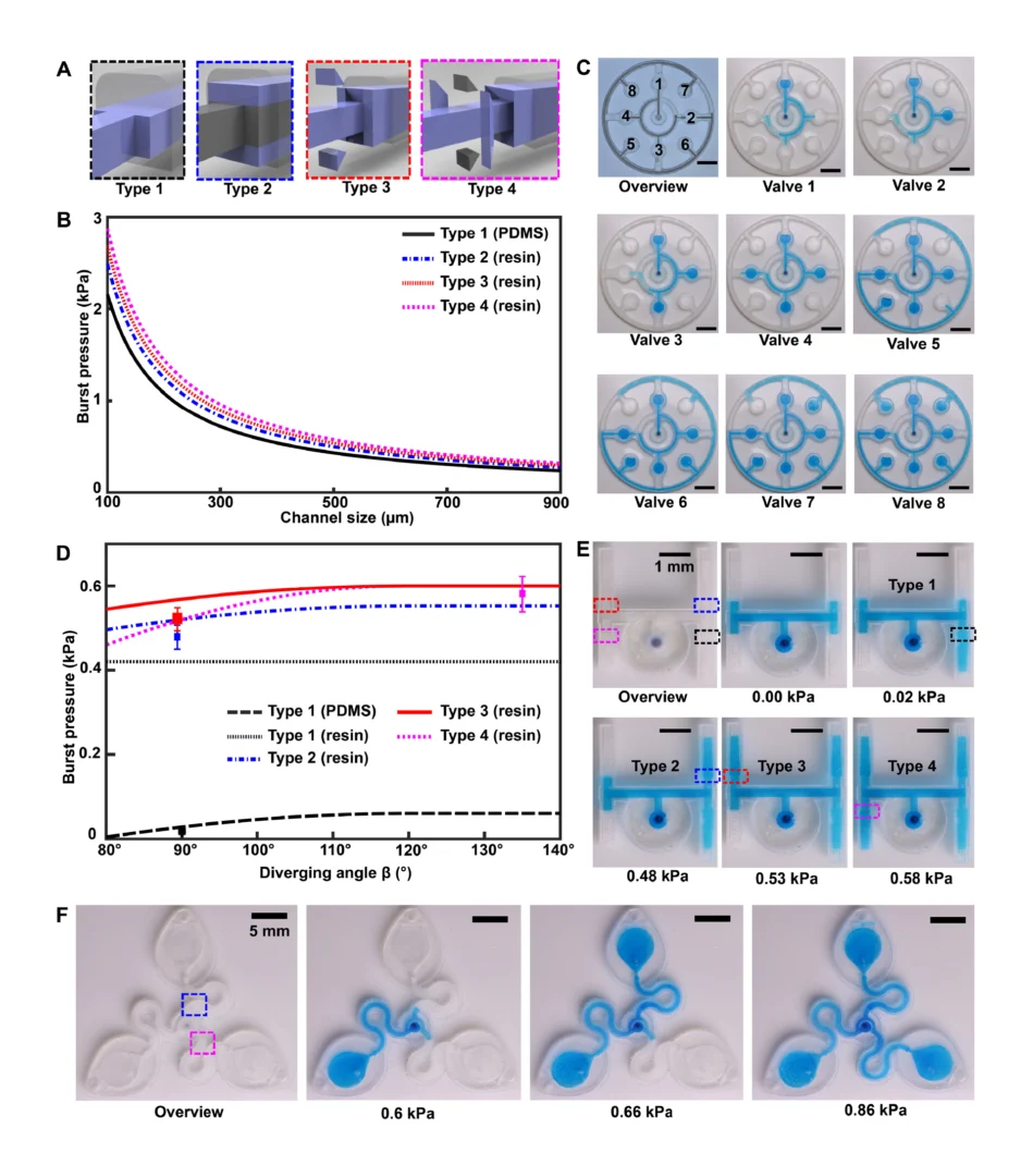
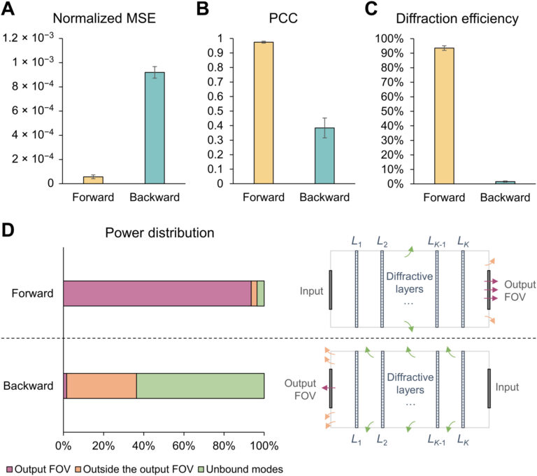
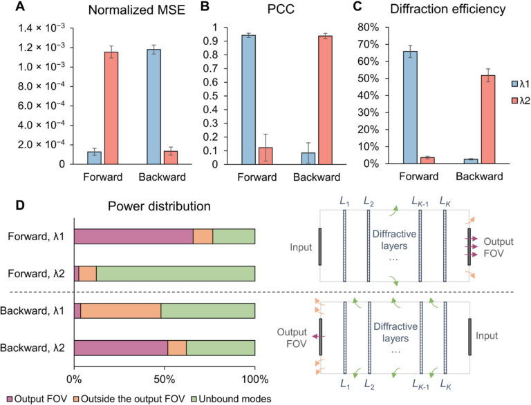
Fig. 10. Performance analysis of the wavelength-multiplexed unidirectional diffractive imager shown in Fig. 9 and fig. S2. (A and B) Normalized MSE (A) and PCC (B) values calculated between the input images and their corresponding diffractive outputs at different wavelengths in the forward and backward operations. (C) The output diffraction efficiencies of the diffractive imager calculated in the forward and backward operations. In (A) to (C), the metrics are benchmarked across the entire MNIST test dataset and shown with their mean values and SDs added as error bars. (D) Left: The power of the different spatial modes at the two wavelengths propagating in the diffractive volume during the forward and backward operations, shown as percentages of the total input power. Right: Schematic of the different spatial modes propagating in the diffractive volume.

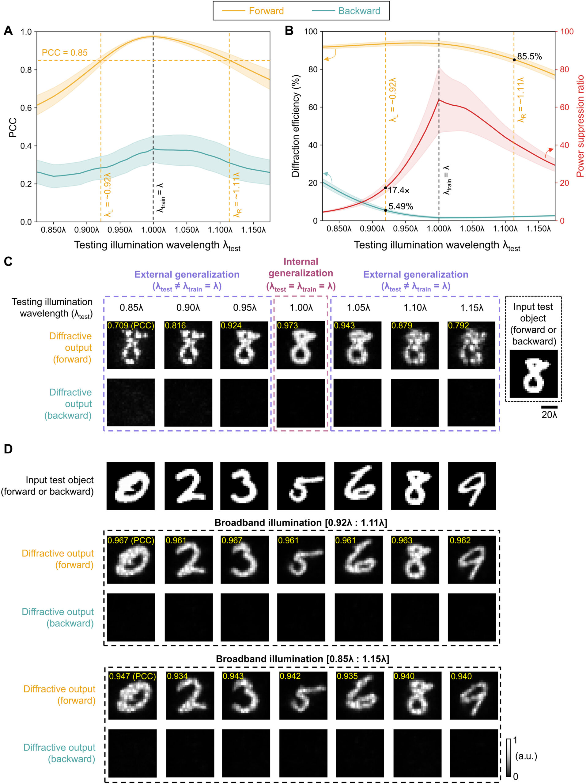
We should also note that, since this wavelength-multiplexed unidirectional imager was trained at two distinct wavelengths that control the opposite directions of imaging, the spectral response of the resulting diffractive imager, after its optimization, is vastly different from the broadband response of the earlier designs, reported in, e.g., Fig. 5. Figure S5 reveals that the wavelength-multiplexed unidirectional imager (as desired and expected) switches its spectral behavior in the range between λ1 and λ2, since its training aimed unidirectional imaging at opposite directions at these two predetermined wavelengths. Therefore, this spectral response that is summarized in fig. S5 is in line with the training goals of this wavelength-multiplexed unidirectional imager. However, it still maintains its unidirectional imaging capability over a range of wavelengths in both directions. For example, fig. S5 reveals that the output image PCC values for A → B remain ≥0.85 within the entire spectral range covered by 0.975 × λ1 to 1.022 × λ1 without any considerable increase in the diffraction efficiency for the reverse path, B → A. Similarly, the output image PCC values for B → A remain ≥0.85 within the entire spectral range covered by 0.968 × λ2 to 1.029 × λ2 without any noticeable increase in the diffraction efficiency for the reverse path, A → B, within the same spectral band. These results highlighted in fig. S5 indicate that the wavelength-multiplexed unidirectional imager can also operate over a continuum of wavelengths around λ1 (A → B) and λ2 (B → A), although the width of these bands are narrower compared to the broadband imaging results reported in Fig. 5.

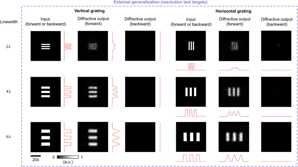
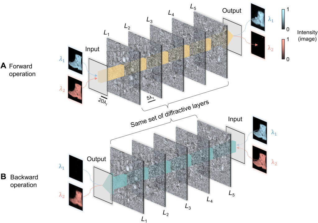
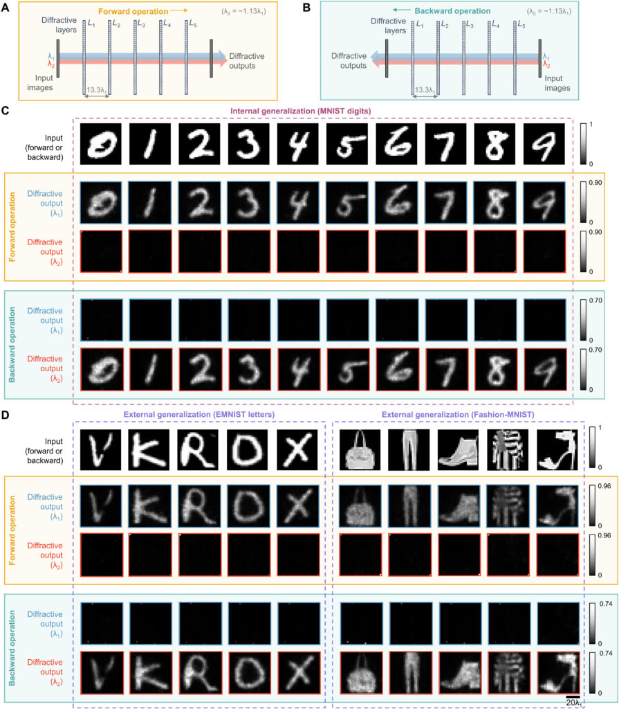
Last, we also tested the external generalization capability of this wavelength-multiplexed unidirectional imager on different datasets: handwritten letter images and fashion products as well as the contrast-reversed versions of these datasets. The corresponding imaging results are shown in Fig. 9D and fig. S6, once again confirming that our diffractive model successfully converged to a data-independent, generic imager where unidirectional imaging of various input objects can be achieved along either the forward or backward directions that can be switched/controlled by the illumination wavelength.

DISCUSSION
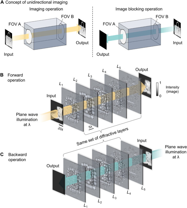
Our results constitute the first demonstration of unidirectional imaging. This framework uses structured materials formed by phase-only diffractive layers optimized through deep learning and does not rely on nonreciprocal components, nonlinear materials, or an external magnetic field bias. Because of the use of isotropic diffractive materials, the operation of our unidirectional imager is insensitive to the polarization of the input light, also preserving the input polarization state at the output. As we reported earlier in Results (Fig. 5), the presented diffractive unidirectional imagers maintain unidirectional imaging functionality under broadband illumination, over a large spectral band that covers, e.g., 0.85 × λ to 1.15 × λ, despite the fact that they were only trained using monochromatic illumination at λ. This broadband imaging performance was further enhanced, covering even larger input bandwidths, by training the diffractive layers of the unidirectional imager using a set of illumination wavelengths randomly sampled from the desired spectral band of operation as illustrated in fig. S7.

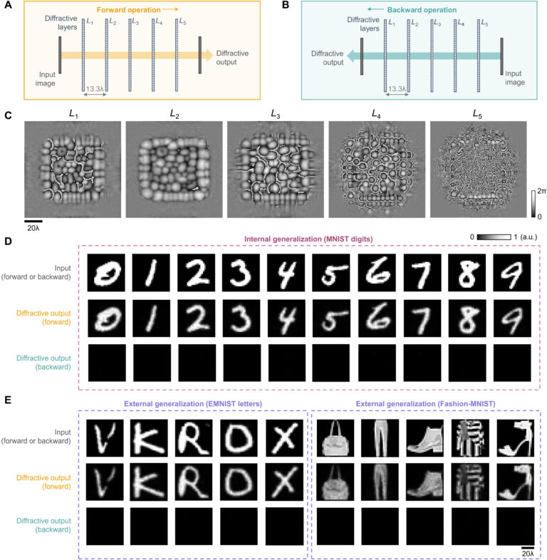
By examining the diffractive unidirectional imager design and the analyses shown in Fig. 2 and fig. S1, one can gain more insights into its operation principles from the perspective of the spatial distribution of the propagating optical fields within the diffractive imager volume. The diffractive layers L1 to L3 shown in Fig. 2C exhibit densely packed phase islands, similar to microlens arrays that communicate between successive layers. Conversely, the diffractive layers L4 and L5 have rapid phase modulation patterns, resulting in high spatial frequency modulation and scattering of light. Consequently, the propagation of light through these diffractive layers in different sequences leads to the modulation of light in an asymmetric manner (A → B versus B → A). To gain more insights into this, we calculated the spatial distributions of the optical fields within the diffractive imager volume in fig. S1 (C and D) for a sample object. We observe that, in the forward direction (A → B), the diffractive layers arranged with the order of L1 to L5 ensured that these optical fields propagated forward through the focusing by the microlens-like phase islands located in the diffractive layers L1 to L3, and as a result, the majority of the input power was maintained within the diffractive volume, creating a power efficient image of the input object at the output FOV. However, for the backward operation (B → A) where the diffractive layers are arranged in the reversed order (L5 to L1), the optical fields in the diffractive volume are initially modulated by the high spatial frequency phase patterns of the diffractive layers (i.e., L5 and L4), and during the early stages of the propagation within the diffractive volume, this leads to a large amount of radiation being channeled to the outer space aside the diffractive volume, in the form of unbound modes (see the green shaded areas in fig. S1, A and B). For the remaining spatial modes that managed to stay within the diffractive volume (propagating from B to A), they were guided by the subsequent diffractive layers (i.e., L3 to L1) to remain outside the output FOV (i.e., ending up within the orange shaded areas in fig. S1B).

One should note that the intensity distributions formed by these modes that lie outside the output FOV can be potentially measured by using, for example, side cameras that capture some of these scrambled modes. Such side cameras, however, cannot directly lead to meaningful, interpretable images of the input objects, as also illustrated in fig. S1. With the precise knowledge of the diffractive layers and their phase profiles and positions, one could potentially train a reconstruction digital neural network to make use of such side-scattered fields to recover the images of the input objects in the reverse direction of the unidirectional imaging system. This “attack” to digitally recover the lost image of the input object through side cameras and learning-based digital image reconstruction methods would not only require precise knowledge of the fabricated diffractive imager but can also be mitigated by surrounding the diffractive layers and the regions that lie outside the image FOV (orange regions in fig. 1, A and B) with absorbing layers/coatings that would protect the unidirectional imager against “hackers,” blocking the measurement of the scattered fields, except the output image aperture. Such absorbing layers also break the time-reversal symmetry of the imaging system, which help mitigate the risk of deciphering and decoding the original input in the backward direction.

Throughout this manuscript, we presented diffractive unidirectional imagers with input and output FOVs that have 28 by 28 pixels, and these designs were based on transmissive diffractive layers, each containing ≤200 by 200 trainable phase-only features. To further enhance the unidirectional imaging performance of these diffractive designs, one strategy would be to create deeper architectures with more diffractive layers, also increasing the total number (N) of trainable features. In general, deeper diffractive architectures present advantages in terms of their learning speed, output power efficiency, transformation accuracy, and spectral multiplexing capability (39, 44, 47, 48). Suppose an increase in the space-bandwidth product (SBP) of the input FOV A (SBPA) and the output FOV B (SBPB) of the unidirectional imager is desired, for example, due to a larger input FOV and/or an improved resolution demand; in that case, this will necessitate an increase in N proportional to SBPA × SBPB, demanding larger degrees of freedom in the diffractive unidirectional imager to maintain the asymmetric optical mode processing over a larger number of input and output pixels. Similarly, the inclusion of additional diffractive layers and features to be jointly optimized would also be beneficial for processing more complex input spectra through diffractive unidirectional imagers. In addition to the wavelength-multiplexed unidirectional imager reported in Figs. 8 to 10, an enhanced spectral processing capability through a deeper diffractive architecture may permit unidirectional imaging with, e.g., a continuum of wavelengths or a set of discrete wavelength across a desired spectral band. Furthermore, by properly adjusting the diffractive layers and the learnable phase features on each layer, our designs can be adapted to input and output FOVs that have different numbers and/or sizes of pixels, enabling the design of unidirectional imagers with a desired magnification or demagnification factor.

Although the presented diffractive unidirectional imagers are based on spatially coherent illumination, they can also be extended to spatially incoherent input fields by following the same design principles and deep learning–based optimization methods presented in this work. Spatially incoherent input radiation can be processed using phase-only diffractive layers optimized through the same loss functions that we used to design unidirectional imagers reported in our Results. For example, each point of the wavefront of an incoherent field can be decomposed, point by point, into a spherical secondary wave, which coherently propagates through the diffractive phase-only layers; the output intensity pattern will be the superposition of the individual intensity patterns generated by all the secondary waves originating from the input plane, forming the incoherent output image. However, the simulation of the propagation of each incoherent field through the diffractive layers requires a considerably increased number of wave propagation steps compared to the spatially coherent input fields, and as a result, the training of spatially incoherent diffractive imagers would take longer.

MATERIALS AND METHODS

Numerical forward model of a diffractive unidirectional imager

In the forward model of our diffractive unidirectional imager design, the input plane, diffractive layers, and output plane are positioned sequentially along the optical axis, where the axial spacing between any two of these layers (including the input and output planes) is set as d. For the numerical and the experimental models used here, the value of d is empirically chosen as 10 and 20 mm, respectively, corresponding to 13.33λ and 26.67λ, where λ = 0.75 mm. In our numerical simulations, the diffractive layers are assumed to be thin optical modulation elements, where the mth neuron on the kth layer at a spatial location (xm, ym, zm) represents a wavelength-dependent complex-valued transmission coefficient, tk, given by

where n(λ) and κ(λ) are the refractive index and the extinction coefficient of the diffractive layer material, respectively; these correspond to the real and imaginary parts of the complex-valued refractive index n~(λ) , i.e., n~(λ)=n(λ)+jκ(λ) (34). For the diffractive unidirectional imager validated experimentally at λ = 0.75 mm, the values of n~(λ) are measured using a terahertz spectroscopy system to reveal n(λ) = 1.700 and κ(λ) = 0.017 for the 3D printing material that we used. The same refractive index value n(λ) = 1.700 is also used in all the diffractive imager models used in our numerical analyses with κ = 0. hkm denotes the thickness value of each diffractive feature on a layer, which can be written as

where hlearnable refers to the learnable thickness value of each diffractive feature and is confined between 0 and hmax. The additional base thickness, hbase, is a constant that serves as the substrate (mechanical) support for the diffractive layers. To constrain the range of hlearnable, an associated latent trainable variable hv was defined using the following analytical form

where Sigmoid(hv) is defined as

Note that before the training starts, hv values of all the diffractive features were initialized as 0. In our implementation, hmax is chosen as 1.07 mm for the diffractive models that use λ = 0.75 mm so that the phase modulation of the diffractive features covers 0 to 2π. For the diffractive imager model that performs wavelength-multiplexed unidirectional imaging, hmax was empirically selected as 1.6 mm, still covering 0 to 2π phase range for both wavelengths (λ1 = 0.75 mm and λ2 = 0.85 mm). The substrate thickness, hbase, was assumed to be 0 in the numerical diffractive models and was chosen as 0.5 mm in the diffractive model used for the experimental validation. The diffractive layers of a unidirectional imager are connected to each other by free space propagation, which is modeled through the Rayleigh-Sommerfeld diffraction equation (33, 49)

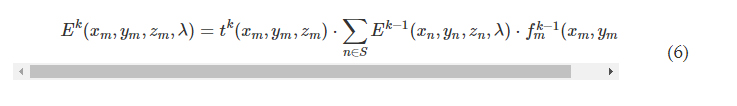
where fkm(x,y,z,λ) is the complex-valued field on the mth pixel of the kth layer at (x, y, z), which can be viewed as a secondary wave generated from the source at (xm, ym, zm), r=(x−xm)2+(y−ym)2+(z−zm)2−−−−−−−−−−−−−−−−−−−−−−−−−−−√ , and j=−1−−−√ . For the kth layer (k ≥ 1, assuming that the input plane is the 0th layer), the modulated optical field Ek at location (xm, ym, zm) is given by

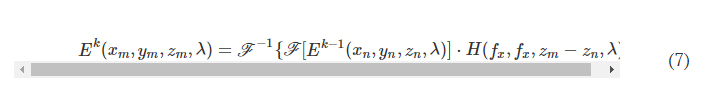
where S denotes all the diffractive features located on the previous diffractive layer. In our implementation, we used the angular spectrum approach (33) to compute Eq. 6, which can be written as

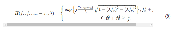
where F and F −1 denote the 2D Fourier transform and the inverse Fourier transform operations, respectively, both implemented using a fast Fourier transform. H(xn, yn, zm − zn, λ) is the transfer function of free space

where fx and fy represent the spatial frequencies along the x and y directions, respectively.

Training loss functions and image quantification metrics

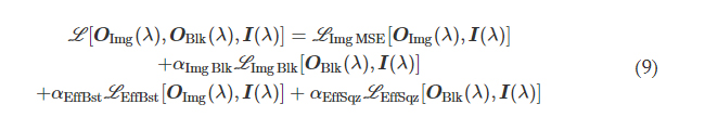
 We first consider a generic form of a diffractive unidirectional imager, where the image formation is permitted in one direction (e.g., A → B), and it is inhibited in the opposite direction (e.g., B → A) at a single training wavelength, λ. The training loss function for such a diffractive unidirectional imager was defined as

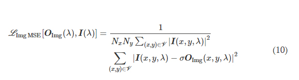
where I(λ) stands for the input image illuminated at a wavelength of λ and OImg(λ) and OBlk(λ) denote the output images in the forward and backward directions, respectively. All the input and output images have the perspective of the illumination beam direction, flipping them left to right as one switches the illumination direction, A → B or B → A. L ImgMSE penalizes the normalized MSE between the OImg(λ) and its ground truth, which can be written as

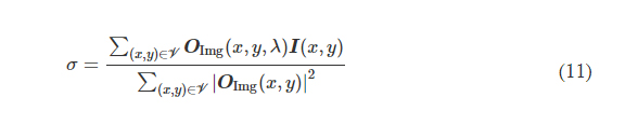
where *(x, y, λ) indexes the individual pixels at spatial coordinates (x, y) and wavelength λ and V denotes the defined FOV that has Nx × Ny pixels at the input or output plane. σ is a normalization constant used to normalize the energy of the diffractive output, thereby ensuring that the computed MSE value is not influenced by the errors arising from the output diffraction efficiency (50), and it is given by the following expression

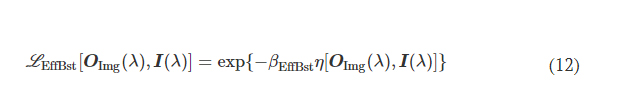
L EffBst is used to improve the output diffraction efficiency along the imaging direction (e.g., A → B), which is defined as

where η(·) is the output diffraction efficiency of the diffractive unidirectional imager and βEffBst is an empirical weight coefficient, which was set as 1.0 during the training of all the diffractive models. η was defined as

L ImgBlk is defined to penalize the structural resemblance between the input image and the diffractive imager output along the image blocking direction (e.g., B → A)

where PCC stands for the Pearson correlation coefficient, defined as

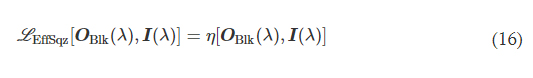
L EffSqz in Eq. 9 is used to penalize the output diffraction efficiency in the backward direction

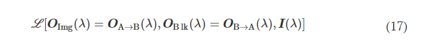
αImgBlk, αEffBst, and αEffSqz in Eq. 9 are the empirical weight coefficients associated with L ImgBlk, L EffBst, and L EffSqz, respectively. We denote the diffractive unidirectional imager output images for A → B and B → A as OA→B(λ) and OB→A(λ), respectively. For the diffractive unidirectional imaging models that were trained using a single illumination wavelength (e.g., in Figs. 2 and 7), the image formation is set to be maintained in the forward direction (A → B) and inhibited in the backward direction (B → A), i.e., OImg(λ) = OA→B(λ) and OBlk(λ) = OB→A(λ). Therefore, the loss function for training these models can be formulated as

where L (·) refers to the same loss function defined in Eq. 9. During the training of the unidirectional imager models with five diffractive layers and a single training wavelength channel, the empirical weight coefficients αImgBlk, αEffBst, and αEffSqz were set as 0, 0.001, and 0.001, respectively; during the training of the other model with three diffractive layers used for the experimental validation, the same weight coefficients were set as 0, 0.01, and 0.003, respectively.

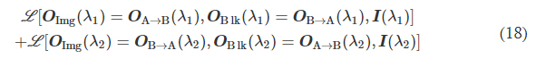
 For the wavelength-multiplexed unidirectional diffractive imager model shown in Fig. 9, at λ1, the image formation is permitted in the direction A → B and inhibited in the direction B → A, whereas at λ2, the image formation is permitted in the direction B → A and inhibited in the direction A → B, respectively; i.e., OImg(λ1) = OA→B(λ1), OBlk(λ1) = OB→A(λ1), OImg(λ2) = OB→A(λ2), and OBlk(λ2) = OA→B(λ2). Accordingly, we formulated the loss function used for training this model as

where L (·) refers to the loss function defined in Eq. 9. During the training of this model, the weight coefficients αImgBlk, αEffBst, and αEffSqz were empirically set as 0.0001, 0.001, and 0.001, respectively.

For quantifying the imaging performance of the presented diffractive imager designs, the reported values of the output MSE, output PCC, and output diffraction efficiency were directly taken from the calculated results of L ImgMSE, PCC, and η, respectively, revealing the averaged values across the blind testing image dataset. When calculating the power distributions of different optical modes within the diffractive volume, the power percentage of the output FOV modes takes the same value as η, and the power percentage outside the output FOV is computed by subtracting the total power integrated within the output image FOV from the total power integrated across the entire output plane. The power in the absorbed modes is calculated by summing up the power loss before and after the optical field modulation by each diffractive layer. After excluding the power of the above modes from the total input power, the remaining part is calculated as the power of the unbound modes.

Training details of the diffractive unidirectional imagers

For the numerical models used here, the smallest sampling period for simulating the complex optical fields is set to be identical to the lateral size of the diffractive features, i.e., ~0.53λ for λ = 0.75 mm. The input/output FOVs of these models (i.e., FOV A and B) share the same size of 44.8 by 44.8 mm2 (i.e., ~59.7λ × 59.7λ) and are discretized into 28 by 28 pixels, where an individual pixel corresponds to a size of 1.6 mm (i.e., ~2.13λ), indicating a four-by-four binning performed on the simulated optical fields.

For the diffractive model used for the experimental validation of unidirectional imaging, the sampling period of the optical fields and the lateral size of the diffractive features are chosen as 0.24 and 0.48 mm, respectively (i.e., 0.32λ and 0.64λ). This also results in a two-by-two binning in the sampling space where an individual feature on the diffractive layers corresponds to four sampling space pixels that share the same dielectric material thickness value. The input and output FOVs of this model (i.e., FOV A and B) share the same size of 36 by 36 mm2 (i.e., 48λ × 48λ) and are sampled into arrays of 15 by 15 pixels, where an individual pixel has a size of 2.4 mm (i.e., 3.2λ), indicating that a 10-by-10 binning is performed at the input/output fields in the numerical simulation.

During the training process of our diffractive models, an image augmentation strategy was also adopted to enhance their generalization capabilities. We implemented random translation, random up-to-down, and random left-to-right flipping of the input images using the transforms.RandomAffine function built-in PyTorch. The translation amount was uniformly sampled within a range of [−10, 10] and [−5, 5] pixels in the diffractive unidirectional imager models used for numerical analysis and the model used for the experimental validation, respectively. The flipping operation is set to be performed at a probability of 0.5.

All the diffractive imager models used in this work were trained using PyTorch (v1.11.0, Meta Platforms Inc.). We selected AdamW optimizer (51, 52), and its parameters were taken as the default values and kept identical in each model. The batch size was set as 32. The learning rate, starting from an initial value of 0.03, was set to decay at a rate of 0.5 every 10 epochs, respectively. The training of the diffractive models was performed with 50 epochs. For the training of our diffractive models, we used a workstation with a GeForce GTX 1080Ti graphical processing unit (Nvidia Inc.) and Core i7-8700 central processing unit (Intel Inc.) and 64 GB of RAM, running Windows 10 operating system (Microsoft Inc.). The typical time required for training a diffractive unidirectional imager is ~3 hours.

Vaccination of the diffractive unidirectional imager against experimental misalignments

During the training of the diffractive unidirectional imager design for experimental validation, possible inaccuracies imposed by the fabrication and/or mechanical assembly processes were taken into account in our numerical model by treating them as random 3D displacements (D) applied to the diffractive layers (53). D can be written as

where Dx and Dy represent the random lateral displacement of a diffractive layer along the x and y directions, respectively, and Dz represents the random perturbation added to the axial spacing between any two adjacent layers (including diffractive layers, input FOV A, and output FOV B). Dx, Dy, and Dz of each diffractive layer were independently sampled based on the following uniform (U) random distributions

where Δ*,tr denotes the maximum amount of shift allowed along the corresponding axis, which was set as Δx,tr = Δy,tr = 0.48 mm (i.e., 0.64λ) and Δz,tr = 1.5 mm (i.e., 2λ) during the training process. Following the training under this vaccination strategy, the resulting diffractive unidirectional imager shows resilience against possible misalignments in the fabrication and assembly of the diffractive layers.

Note that, in addition to the 3D displacements of the diffractive layers, there may also exist other types of alignment errors in our experimental setup, such as 3D rotational misalignments of the diffractive layers. However, since the holders used to fix the diffractive layers are, in general, manufactured with high structural precision and surface flatness, we did not incorporate these types of misalignments into our forward model considering their negligible impact in our case. In the event that such rotational misalignments of the diffractive layer become an important factor in the experimental results, the undesired in-plane rotations of the diffractive layers can be readily modeled through applying a 2D coordinate transformation based on unitary rotation matrices, while the out-of-plane rotation of the diffractive layers can be addressed by modifications to the formulation of the wave propagation between tilted diffractive planes (53–55).

Experimental terahertz imaging setup

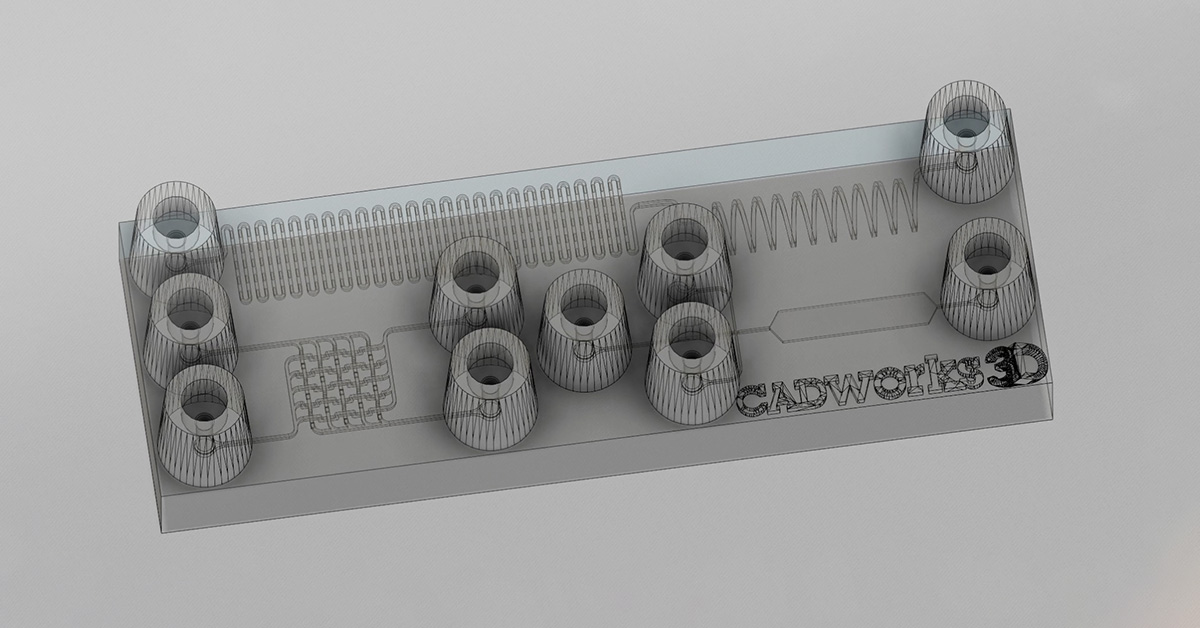
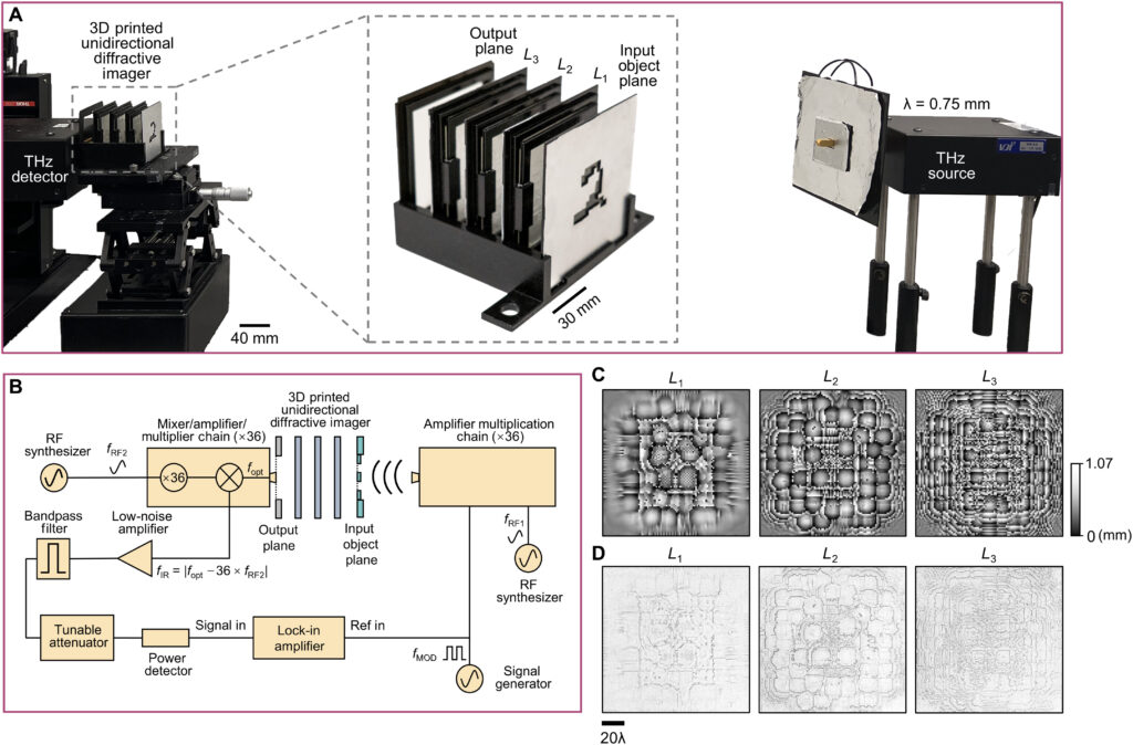
We fabricated the diffractive layers using a 3D printer (PR110, CADworks3D). The test objects were also 3D printed (Objet30 Pro, Stratasys) and coated with aluminum foil to define the light-blocking areas, with the remaining openings defining the transmission areas. We used a holder that was also 3D printed (Objet30 Pro, Stratasys) to assemble the printed diffractive layers along with input objects, following the relative positions of these components in our numerical design.

A terahertz continuous-wave scanning system was used for testing our diffractive unidirectional imager design. According to the experimental setup illustrated in Fig. 6B, we used a terahertz source in form of a WR2.2 modular amplifier/multiplier chain (AMC), followed by a compatible diagonal horn antenna (Virginia Diodes Inc.). A 10-dBm radiofrequency (RF) input signal at 11.1111 GHz (fRF1) at the input of AMC is multiplied 36 times to generate the output radiation at 400 GHz, corresponding to a wavelength of λ = 0.75 mm. The AMC output was also modulated with a 1-kHz square wave for lock-in detection. The assembled diffractive unidirectional imager is placed ∼600 mm away from the exit aperture of the horn antenna, which results in an approximately uniform plane wave impinging on its input FOV (A) with a size of 36 by 36 mm2 (i.e., 48λ × 48λ). The intensity distribution within the output FOV (B) of the diffractive unidirectional imager was scanned at a step size of 1 mm by a single-pixel mixer/AMC (Virginia Diodes Inc.) detector on an xy positioning stage that was built by combining two linear motorized stages (Thorlabs NRT100). The detector also receives a 10-dBm sinusoidal signal at 11.083 GHz (fRF2) as a local oscillator for mixing to down-convert the output signal to 1 GHz. The signal is then fed into a low-noise amplifier (Mini-Circuits ZRL-1150-LN+) with a gain of 80 dBm, followed by a band-pass filter at 1 GHz (± 10 MHz) (KL Electronics 3C40-1000/T10-O/O), so that the noise components coming from unwanted frequency bands can be mitigated. Then, after passing through a tunable attenuator (HP 8495B) used for linear calibration, the final signal is sent to a low-noise power detector (Mini-Circuits ZX47-60). The detector output voltage is measured by a lock-in amplifier (Stanford Research SR830) with the 1-kHz square wave used as the reference signal. Last, the lock-in amplifier readings were calibrated into a linear scale. In our postprocessing, linear interpolation was applied to each measurement of the intensity field to match the pixel size of the output FOV (B) used in the design phase, resulting in the output measurement images shown in Fig. 7C.
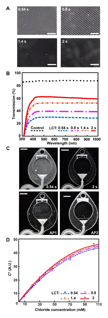
Materials