An Optimization Framework for Silicon Photonic Evanescent-Field Biosensors Using Sub-Wavelength Gratings

An Optimization Framework for Silicon Photonic Evanescent-Field Biosensors Using Sub-Wavelength Gratings

Lauren S. Puumala, Samantha M. Grist, Kithmin Wickremasinghe, Mohammed A. Al-Qadasi, Sheri Jahan Chowdhury, Yifei Liu, Matthew Mitchell, Lukas Chrostowski, Sudip Shekhar,and Karen C. Cheung

Silicon photonic (SiP) evanescent-field biosensors aim to combine the information-rich readouts offered by lab-scale diagnostics, at a significantly lower cost, and with the portability and rapid time to result offered by paper-based assays. While SiP biosensors fabricated with conventional strip waveguides can offer good sensitivity for label-free detection in some applications, there is still opportunity for improvement. Efforts have been made to design higher-sensitivity SiP sensors with alternative waveguide geometries, including sub-wavelength gratings (SWGs). However, SWG-based devices are fragile and prone to damage, limiting their suitability for scalable and portable sensing. Here, we investigate SiP microring resonator sensors designed with SWG waveguides that contain a “fishbone” and highlight the improved robustness offered by this design. We present a framework for optimizing fishbone-style SWG waveguide geometries based on numerical simulations, then experimentally measure the performance of ring resonator sensors fabricated with the optimized waveguides, targeting operation in the O-band and C-band. For the O-band and C-band devices, we report bulk sensitivities up to 349 nm/RIU and 438 nm/RIU, respectively, and intrinsic limits of detection as low as 5.1 × 10⁻⁴ RIU and 7.1 × 10⁻⁴ RIU, respectively. This performance is comparable to the state of the art in SWG-based sensors, positioning fishbone SWG resonators as an attractive, more robust, alternative to conventional SWG designs. 

Keywords: silicon photonics, evanescent field biosensor, SOI biosensor, ring resonator, fishbone sub-wavelength grating waveguide, sub-wavelength grating waveguide, SWG-assist waveguide, bridged SWG waveguide, microfluidics

We kindly thank the University of British Columbia for this collaboration, and for sharing the results obtained with their system.

Introduction

The recent COVID-19 pandemic has highlighted the importance of scalable, rapid, portable, and cost-effective medical diagnostics in public safety and informed decision making [1,2]. Currently, gold-standard medical diagnostics rely on lab-based tests, which are performed in centralized settings and suffer from high costs, long analysis times, the requirement for highly trained operators, and complex logistics regarding sample transport and information management [3]. Portable, low-cost, and easy-to-use diagnostic tools, such as paper-based assays, allow for rapid and accessible testing in decentralized settings. However, they offer less information-rich readouts and often suffer from poorer sensitivity and accuracy compared with lab-based techniques [4]. Silicon photonic (SiP) biosensors offer the potential to bridge the gap between these two classes of diagnostic systems.

By leveraging highly scalable complementary metal-oxide semiconductor (CMOS) fabrication processes, SiP chips can be produced in high volumes at low cost [5,6,7,8]. Their scalability, affordability, rapid readout, and millimeter-scale form factor, makes SiP sensors amenable to testing in point-of-care (POC) settings. In addition to managing infectious diseases, rapid POC testing is valuable for the diagnosis of conditions such as stroke and sepsis, where rapid confirmation of clinical findings is critical for timely and effective treatment decision-making [9,10,11]. POC tests can also improve access to diagnostics in remote and resource-limited communities. Dozens of sensors can be fabricated on a single SiP chip, which, when combined with spatially controlled functionalization, can facilitate high-throughput multiplexed diagnostic testing [12]. This opens opportunities for more selective and information-rich diagnosis of conditions that are challenging to identify based on a single biomarker alone [9,13]. Extremely sensitive biomarker detection down to the pg/mL scale has been demonstrated on SiP platforms based on well-established strip waveguides (Figure 1c) [14,15]. However, these exceptionally low-limit of detection demonstrations have used sandwich assay formats in which the final detected signal originated from a detection antibody [16] or subsequent amplification step [14,15], rather than from the analyte itself. Label-based strategies such as these offer slower detection and require more complex assay operation than label-free formats. While label-free detection has been demonstrated with SiP platforms [17,18] and is more suitable for POC applications due to its simplicity, label-free biosensors based on strip waveguides typically have higher detection limits in the ng/mL range. Many clinical diagnostic assays require lower detection limits [19]. This has motivated the design of SiP sensors, such as microring resonators (MRRs), with improved performance criteria, including refractive index sensitivities.

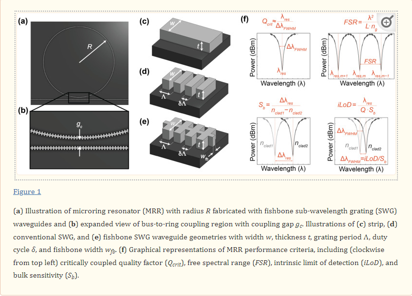
MRRs use their sensitivity to surface and cladding refractive index changes to detect analytes, such as disease biomarkers, captured on the sensor surface. These MRR structures consist of a waveguide that is looped back on itself in a ring and a straight bus waveguide that couples light into the ring (Figure 1a) [20,21]. The ring and bus waveguides are separated by a defined coupling gap distance, gc, which controls the amount of light coupled into the ring (Figure 1b). Resonance occurs when the optical path length of the ring is equal to an integer multiple of the wavelength of light in the waveguide. These devices support resonances at wavelengths, λres, given by

where neff is the effective refractive index of the waveguide, L is the resonator length (L=2πR) for a circular MRR with radius, (R), and m is an integer number representing the order of interference. A portion of the electric field, called the evanescent field, travels outside of the waveguide and interacts with the surrounding material, or analyte. This creates a thin refractive index-sensitive region that extends up to a few hundred nanometers outside of the waveguide [22]. A change in the refractive index surrounding the resonator, for example due to biomolecule binding, changes the neff, leading to a shift in λres. Several strategies are available for tracking the resonance shifts. A simplistic setup comprises a broadband optical source that provides a continuous spectrum of wavelengths and a spectrum analyzer to measure the magnitude of the transmission versus wavelength [23]. Another approach uses a combination of a tunable laser and a photodetector to scan the input wavelength and read the output intensity, respectively [1,24,25]. However, another compact and cost-effective approach recently proposed by Chrostowski et al. [1] replaces off-chip tunable lasers with a chip-integrated fixed wavelength laser. In-resonator phase shifters [26] are used to tune the resonance, and the transmission is read out using a photodetector.

Three metrics that are particularly valuable for evaluating SiP sensor performance and comparing different resonator architectures are the bulk sensitivity, Sb, quality factor, Q, and intrinsic limit of detection, iLoD [21,27]. The bulk sensitivity is defined as the change in λres for a one unit change in the bulk refractive index [27]:

where ng is the group index and ∂neff/∂nbulk is the index susceptibility and relates to the portion of the optical mode that interacts with the analyte [21]. Experimentally, Sb can be obtained by exposing the sensor to several solutions having different known refractive indices and tracking the corresponding resonance peak shifts. Often, aqueous solutions prepared with different concentrations of salt [19], isopropanol [3], or glycerol [28,29] are used. Sb is then calculated from the slope of the resonance peak shifts plotted against the bulk refractive index.

The quality factor is a dimensionless quantity that represents a photon’s lifetime in the resonator and is the number of oscillations required for the photon’s energy to decay to 1/e [21,22,27]. A high quality factor indicates that light present in the resonator interacts with the analyte for a greater amount of time, and is desirable because it improves the resolution to which the resonance peak shifts can be resolved and reduces the impact of the intensity noise on the resolved shifts [21,22,27,30,31]. The quality factor depends on the total distributed optical losses in the resonator, α (dB/m), and can be calculated according to Equation (3) [27].

For MRRs, light must be coupled out of the resonator to observe a resonance change, which degrades the quality factor. In the critically coupled condition, the quality factor is degraded by half compared with the intrinsic quality factor represented by Equation (3), because the proportion of the power coupled out of the resonator is equal to the round-trip loss, effectively doubling the total lost power with each resonator round trip [21]. As such, the critically coupled quality factor is a more useful metric for MRR sensors. Experimentally, it can be approximated based on the full width at half maximum (FWHM) at resonance (ΔλFWHM) according to Equation (4) [21,22].

Materials

Master Mold Resin

ProFluidics 285D

Finally, the iLoD is a figure of merit introduced to objectively compare sensors, independent of their experimental setups, functionalization strategies, and assays [21,22,27,32]. Unlike the system limit of detection (sLoD (RIU)) [21] or analyte limits of detection (M or g/mL) [22], it depends only on the intrinsic characteristics of the resonator and represents the minimum refractive index unit change (in RIU) required to shift the resonance wavelength by ΔλFWHM. It is given by Equation (5) [21,22].

Accordingly, Sb and Q should be maximized for optimal sensor performance. Resonators designed with conventional strip waveguides (Figure 1c) operating in the quasi-transverse electric mode (hereafter referred to as the TE mode for brevity) can achieve very low optical losses, and therefore, high quality factors [33]. However, the high index contrast between the silicon waveguide and cladding material (typically aqueous solutions for biosensing applications) results in strong confinement of the electric field in the waveguide core. This results in little overlap between the evanescent field and analyte, limiting Sb [3]. Different waveguide designs have been investigated to achieve higher sensitivities, including thin strip waveguides [34], strip waveguides operating in the quasi-transverse magnetic (TM) mode (hereafter referred to as the TM mode for brevity) [21,35], and slot waveguides [36,37].

Sub-wavelength grating (SWG) waveguides (Figure 1d) are yet another geometry that has demonstrated considerable sensitivity enhancements compared to strip waveguides operating with both TE and TM polarizations [38]. SWGs are periodic structures that consist of silicon blocks, interspaced with a lower refractive index material, such as the cladding material (e.g., air [39], water [6,19,40], or a polymer such as SU8 [41]). SWG structures significantly extend the SiP design space by allowing for the fabrication of metamaterial anisotropic structures using standard single-etch CMOS-compatible techniques [42]. SWGs have been used to create photonic structures with tailored modal confinement, broadband behavior, dispersion control, and polarization management [42,43]. For example, the tailorability of modal confinement in SWGs has allowed for the design of ultralow loss waveguide crossings [41] and efficient couplers to interface on-chip waveguides with off-chip optical fibers [44]. The tailorable modal confinement and diffraction suppression afforded by SWGs have been employed to design ultracompact and broadband Y-branches [45] and adiabatic couplers [46,47]. Further, the controlled dispersion of SWGs has been leveraged to design broadband 2 × 2 interferometric switching cells [43] and broadband directional couplers [48,49]. Finally, SWG structures have been used to design optimized sensing waveguides [42]. These periodic SWG structures behave as waveguides below the Bragg threshold where the grating period, Λ, is less than half the effective wavelength of light in the waveguide (Λ<<λ2neff) [5,38,41,50]. The optical properties (e.g., neff, ng) of the SWG are highly tunable and depend on the waveguide width (w), thickness (t), and duty cycle (δ, the ratio of the silicon block length to the grating period), in addition to the grating period (Figure 1d). Compared with strip waveguides, SWGs can offer reduced electric field confinement in the waveguide core, which increases light interaction with the analyte [6]. As such, MRRs can be fabricated with SWGs for improved bulk refractive index sensitivity Sb. In the literature, many SWG waveguide variants have been used in MRR and racetrack resonator (RTR) sensors, including SWGs that operate in the transverse electric (TE) [19,21,29,39] and transverse magnetic (TM) [51,52] modes, trapezoidal pillar SWGs [53], substrate overetch (SOE) SWGs [6], pedestal SWGs with undercut etching [28], single- and double-slot SWGs [54,55], and multibox SWGs [3].

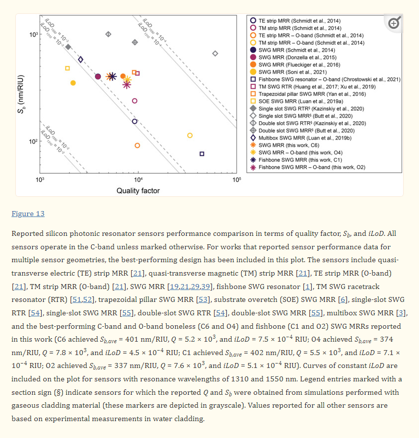
When used for biosensing applications, a major limitation of these SWG waveguides, which are composed of isolated silicon blocks, is that they are fragile and susceptible to damage during and after manufacturing [1]. In contrast to other SWG devices (e.g., waveguide crossings, Y-branches, adiabatic couplers, and directional couplers) which are often clad with silicon dioxide, an oxide-open etch is typically necessary to expose SWG-based sensors to the analyte solution [56]. This oxide-open etch can cause delamination of the fragile silicon blocks that make up the SWG waveguides from the sensor substrate [1]. The exposed SWG waveguides can also be damaged during surface functionalization processes and binding assays [57,58,59]. This hinders the fabricability and robustness of SWG-based biosensors, complicating their translation to scalable POC sensors. One solution is to add a fishbone to the SWG waveguide (Figure 1e), which turns the waveguide into a single piece of silicon [1,60,61,62]. This lowers the risk of delamination and improves fabricability, while maintaining the sensitivity enhancements offered by the SWG design. As an additional advantage, the fishbone eliminates discontinuities in tapers which convert routing waveguides to the SWG bus region, reducing reflections and optical losses at the taper interface [1]. To our knowledge, only two other works have reported the design and fabrication of sensors based on fishbone SWG structures [1,62]. Bickford et al. [62] designed Mach-Zehnder interferometers based on fishbone SWG waveguides and presented their transmission spectra, but did not quantify device performance in terms of Q, Sb, or iLoD. Chrostowski et al. [1] designed a resonator with integrated photoconductive waveguide heater detectors for operation with a fixed-wavelength laser. A fraction of the resonator consisted of a fishbone SWG waveguide. This device achieved an experimental quality factor of 4.44 × 10⁴ and a simulated bulk sensitivity of 76.0 nm/RIU, yielding an estimated iLoD of 3.77 × 10⁻⁴ RIU. No existing works have reported the experimental sensitivity of fishbone SWG sensors. Moreover, to the best of our knowledge, no previous works have demonstrated a comprehensive optimization of the fishbone SWG waveguide geometry for sensing in terms of duty cycle, fishbone width, and grating period.

In this work, we present a novel framework for using numerical simulations to optimize fishbone SWG waveguides for high sensitivity MRRs, aiming to achieve comparable sensing performance to previously reported MRRs based on non-fishbone SWG waveguides, but with improved robustness. For the first time, we demonstrate the experimental performance of MRRs entirely fabricated with fishbone SWG waveguides and compare them to boneless SWG MRRs in terms of the key sensor performance metrics Qcrit (hereafter, simply referred to as Q), Sb, and iLoD. While the full function of a biosensor depends on several factors beyond the transducer itself, including the functionalization chemistry and assay design, characterizing the intrinsic resonator performance based on these metrics is essential to drawing fair comparisons to other transducers. In both simulations and experiments, we target sensor operation in the O-band (1260–1360 nm) and C-band (1530–1565 nm). While most SiP applications use C-band light, the O-band offers lower optical losses due to reduced water absorption, which has the potential to enhance sensor performance by improving Q [21]. To our knowledge, this is the first demonstration of any SWG ring resonators using O-band light for liquid-phase sensing. This is a valuable contribution in the context of POC biosensing, as compact O-band lasers are less expensive and easier to manufacture than C-band ones [1,63], making O-band systems more suitable for affordable and scalable SiP biosensing platforms. Lastly, we compare the performance of our fishbone SWG MRRs to other SWG sensors reported in the literature. This thorough optimization and experimental characterization of fishbone SWG MRRs is an important step toward designing sensitive SiP biosensing platforms that are practical for the POC. In the future, we envision that these sensors can be used for robust biosensing in applications such as the detection of cancer [14,15,16,17,64], inflammation [65], cardiac disorders [66,67], viral infection [68], bacteria [69], and toxins [70,71].

2. Materials and Methods

2.1. Numerical Models

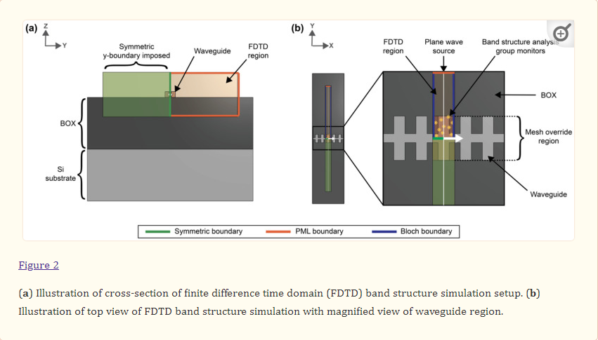
2.1.1. Index and Bulk Sensitivity Simulations Finite difference time domain (FDTD) simulations were performed using FDTD Solutions from Lumerical (Ansys, Inc., Canonsburg, PA, USA). In these simulations, one unit cell of a SWG waveguide was modeled with Bloch boundary conditions. The periodicity of SWG waveguides permits the use of band structure simulations for reduced simulation time compared to discrete time domain calculations. This method has been widely used to simulate structures such as photonic crystals [19,72]. In this method, light is injected into the structure over the frequency range of interest and the time-dependent response of the structure is recorded for a range of swept wavevector values [73]. Spectral analysis is performed on this response by searching for local maxima and plotting them in the frequency domain to provide the band structure. Using linear regression to fit the band structure curve, the ratio of the angular velocity to the wavevector is obtained as well as higher order terms. This helps extract the phase and group velocities (vp and vg, respectively) from which the effective and group indices are calculated, according to Equations (6)–(8) [74,75],

where ω is the angular frequency, kx is the wavenumber, and c is the speed of light in a vacuum. To set up these simulations, the silicon SWG waveguide was drawn on top of a 2 µm-thick SiO2 buried oxide (BOX) layer with a silicon wafer layer beneath (Figure 2). Water was used as the background (cladding) material. Multi-coefficient material models based on empirical complex refractive index data available from the Lumerical Material Database were used for the simulations [76,77]. The software’s default material model fitting parameters were used for silicon and SiO2. As Lumerical’s default fitting parameters yielded an unsatisfying fit for the complex refractive index of water over the O- to C-band wavelength range (Figure S1a), the fit tolerance for this material was reduced to 1 × 10⁻⁶ with the maximum coefficients parameter set to 10 [78]. To better capture the absorption losses of the water cladding, the imaginary weight was increased to 100. This meant that the fitting routine gave 100 times more consideration to the imaginary part of the complex refractive index than the real part; increasing the imaginary weight is recommended when the imaginary refractive index is much smaller than the real refractive index [78]. This produced a model that accurately fit the empirical refractive index data (Figure S1b). Light was set to propagate along the x-axis. The FDTD simulation region enclosed one unit cell of the SWG waveguide in the x-direction and extended 0.75 µm above and below the waveguide in the z-direction and 3 µm on either side of the waveguide in the y-direction. These boundary locations were selected based on convergence testing. Bloch boundary conditions were used for the x boundaries. Perfectly matched layers (PML) were used for the z boundaries and one of the y boundaries to absorb waves propagating outwards and avoid reflections, whereas an anti-symmetric condition was used for the other y boundary to reduce the simulation time. The global mesh accuracy was set to 4 and an override mesh (dx = 0.01 µm, dy = 0.02 µm, dz = 0.02 µm) was included in the FDTD region immediately around the waveguide (dimensions defined by Λ × w × t). A plane wave source was used to inject light into the structure over a frequency range of 120–270 THz (corresponding to a wavelength range of 1111–2500 nm) to cover the O-C band spectra. A band structure analysis group was set up in the FDTD region with ten time monitors randomly distributed in the waveguide.

The effective index and group index versus wavelength were then calculated by sweeping kx across ten evenly spaced values within a specified range. For a given SWG waveguide geometry, this range was defined by firstly running a coarse sweep with a kx range of 0.1–0.5 in order to extract the kx values that corresponded to neff at 1310 nm and 1550 nm according to kx=neffΛ/λ. These values helped define a narrower simulation range with an added buffer of 0.02, which ran with a finer 10-point sweep. 2.1.2. Propagation Loss Simulations A similar band structure FDTD simulation method to that described in Section 2.1.1 was used to estimate the propagation losses of the SWG waveguides [72]. For these simulations, however, a dipole cloud light source was used to inject light into the structure over a 1-THz frequency range about the operating frequency. For operation in the C-band at 1550 nm, a frequency range of 193.05–194.05 THz (corresponding to a wavelength range of 1546–1554 nm) was used, whereas for operation in the O-band at 1310 nm, a frequency range of 228.51–229.51 THz (corresponding to a wavelength range of 1307–1313 nm) was used. A field decay analysis group was added to the simulation, which included two time monitors placed at different points along the waveguide. The field decay along the waveguide, captured by the time monitors, and the group velocity, obtained from the FDTD simulations described in Section 2.1.1, were used to calculate the propagation loss, α (dB/m), according to Equation (9):The effective index and group index versus wavelength were then calculated by sweeping kx across ten evenly spaced values within a specified range. For a given SWG waveguide geometry, this range was defined by firstly running a coarse sweep with a kx range of 0.1–0.5 in order to extract the kx values that corresponded to neff at 1310 nm and 1550 nm according to kx=neffΛ/λ. These values helped define a narrower simulation range with an added buffer of 0.02, which ran with a finer 10-point sweep.

2.1.2. Propagation Loss Simulations A similar band structure FDTD simulation method to that described in Section 2.1.1 was used to estimate the propagation losses of the SWG waveguides [72]. For these simulations, however, a dipole cloud light source was used to inject light into the structure over a 1-THz frequency range about the operating frequency. For operation in the C-band at 1550 nm, a frequency range of 193.05–194.05 THz (corresponding to a wavelength range of 1546–1554 nm) was used, whereas for operation in the O-band at 1310 nm, a frequency range of 228.51–229.51 THz (corresponding to a wavelength range of 1307–1313 nm) was used. A field decay analysis group was added to the simulation, which included two time monitors placed at different points along the waveguide. The field decay along the waveguide, captured by the time monitors, and the group velocity, obtained from the FDTD simulations described in Section 2.1.1, were used to calculate the propagation loss, α (dB/m), according to Equation (9):

where β (Np/s) is the slope of the field decay over time obtained from the simulation (1 Np=20⋅log10(e) dB) [79]. In these loss simulations, the z-span of the FDTD region and override mesh were extended to 3 µm above and below the waveguide. This reduced the risk of losses to the PML boundaries and extended the simulation region into the silicon wafer below the BOX to account for optical losses due to leakage to the substrate. As these simulations were less time-consuming than the sweeps described in Section 2.1.1, the global mesh accuracy was increased to 6 and the override mesh accuracy was increased (dx, dy, dz = 0.01 µm) to improve the simulation accuracy. For each SWG geometry, the loss simulations were performed using the kx value corresponding to the effective index of the structure simulated in Section 2.1.1.

2.2. Design and Optimization of Fishbone SWG Waveguides

In order to optimize fishbone SWG waveguides for sensing applications and compare their performance to conventional boneless SWG waveguides, we performed fully vectorial 3D-FDTD band structure simulations using Bloch boundary conditions, as described in Section 2.1.1. These simulations were used to predict the effective index, neff, and bulk sensitivity, Sb, of SWG waveguides operating with C-band and O-band light in the TE mode. Compared to Sb, surface sensitivity (Ss) is the more important metric for biosensors in the study of target molecule quantification, but it must be defined for a specific molecule of interest, meaning that Sb is a more suitable criterion for the general comparison of sensors when the target is unknown or the sensors are used for different biosensing assays [3,40]. As such, Sb was used in this work to compare sensing architectures. For all simulations, a waveguide width of 500 nm, waveguide thickness of 220 nm, and BOX thickness of 2 µm, were used. The grating period, Λ, was initially fixed at 250 nm. This grating period was selected, as it is below the Bragg threshold (Λ << λ/2neff) for all studied geometries. Further, others [19,39] have studied boneless SWG waveguides with this grating period, providing a valuable benchmark for comparison. The waveguides were optimized by performing simulation sweeps in which the duty cycle, δ, was varied from 0.2 to 0.8 for SWGs with fishbone widths, wfb, of 0, 60, 100, 140, 180, and 220 nm. Simulations performed with water cladding were used to extract neff and the group index, ng, for each waveguide geometry. To extract Sb, band structure simulations were additionally performed using an index-shifted water cladding material to simulate a dilute salt solution. For this index-shifted material, the real part of the refractive index of water was shifted by 0.01 (Δnbulk) at all wavelengths in the water material model; it was assumed that material absorption, and therefore, the imaginary term of the refractive index, remained constant. By simulating neff in both materials to extract Δneff, the susceptibility, ∂neff/∂nbulk, could be estimated as Δneff/Δnbulk. Using this susceptibility alongside the group index, Sb was calculated according to Equation (2). 

Figure 3 presents the results of these simulations. Increasing δ and wfb led to an increase in neff for the C-band and O-band structures. This reflects an increase in light confinement as the volume fraction of silicon in the SWG structure increases. This increased light confinement decreases the interaction of light with the bulk material. As seen in Figure 3, this is generally accompanied by a decrease in Sb. However, when neff approaches and falls below ~1.44, which is the refractive index of the BOX, the waveguide no longer effectively guides light, and a considerable decrease in Sb is observed when δ and wfb are decreased further [74]. For the C-band devices, the greatest value of Sb out of all the simulated structures was roughly 470 nm/RIU, whereas that for the O-band devices was roughly 400 nm/RIU. The greater sensitivities of the C-band structures can be attributed to lower mode confinement at longer wavelengths at the defined waveguide geometry of w = 500 nm and t = 220 nm [20].

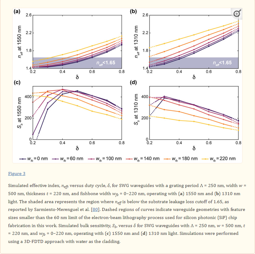
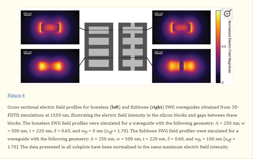
The sensitivity results highlight that fishbone SWG waveguides can achieve comparable sensitivities compared with boneless SWG waveguides for appropriate combinations of δ and wfb. For both fishbone and boneless SWG structures, the electric field is highly concentrated in the gaps between the silicon blocks, as shown in Figure 4. This allows for strong interaction between the evanescent field and the bulk medium.

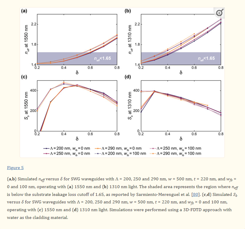
Next, to investigate the effect of Λ on the waveguide performance, band structure simulations were performed in which the duty cycle was varied from 0.2 to 0.8 for SWGs with Λ = 200, 250, and 290 nm. These simulations were performed with wfb = 0 and 100 nm to analyze the effect of Λ on both conventional and fishbone SWGs. The results of these simulations are presented in Figure 5. Note that O-band simulation results are not presented for the fishbone waveguide at δ = 0.7 and 0.8 for Λ = 290, nor are they presented for the boneless waveguide at δ = 0.8 for Λ = 290, as these structures exceed the Bragg threshold. For the C-band devices, neff and Sb are nearly constant across all three values of Λ for a given δ and wfb. Similarly, for the O-band devices, Λ had a small effect on neff and Sb, however a small increase in neff is seen with increasing Λ, particularly for waveguides approaching the Bragg threshold. Nevertheless, below the Bragg limit, the effect of Λ on the simulated waveguide performance is much less pronounced than the effect of δ and wfb. This is consistent with observations regarding the accuracy of the equivalent refractive index method in predicting SWG behavior well below the Bragg threshold [38,50,81]. The equivalent refractive index method approximates the SWG as a homogeneous strip waveguide with an equivalent refractive index, neq, given by Rytov’s formula, n2eq≈δn2Si+(1−δ)n2clad, where nSi and nclad are the refractive indices of the silicon blocks and the cladding material, respectively [38,50]. Using this method, less computationally taxing 2D simulations can be used to estimate the optical properties of the waveguide (e.g., neff, ng, Sb, and α) [19]. It has been reported that this method provides suitable approximations for SWG structures in the deep-SWG regime, which is well below the Bragg threshold [37,41]. As neq is independent of Λ for any given δ, in this regime, the waveguide’s optical properties are, therefore, relatively insensitive to Λ. However, the accuracy of this model degrades near the Bragg threshold, and accurate analysis of the waveguide requires 3D analysis of the periodic geometry and the propagating Bloch–Floquet modes [19,50]. Therefore, near the Bragg threshold, it can no longer be assumed that neff and Sb are independent of Λ, which supports the results illustrated in Figure 5.

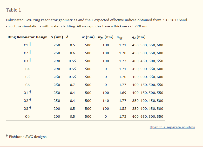
Based on this analysis, we selected two C-band and two O-band fishbone SWG waveguide designs for fabrication. Given the small effect of Λ on waveguide performance, we chose devices with Λ = 250 nm. Three evaluation criteria were used to select the best combinations of δ and wfb for the fabricated structures. First, the minimum feature size had to exceed 60 nm, which was the minimum fabricable feature size of the ANT electron-beam foundry process used in this work [82]. Next, the reduced modal confinement of SWG waveguides can lead to considerable optical losses to the substrate [3,80]. Sarmiento-Merenguel et al. reported that these substrate leakage losses are independent of SWG geometry and established a direct relationship between leakage losses and neff, along with practical design guidelines [80]. In particular, for a 2 µm BOX layer, for C-band light, substrate leakage losses are negligible when neff > 1.65. Therefore, in this work, only fishbone SWG designs with simulated neff values above this cutoff were considered for fabrication. It should be noted that this leakage loss cutoff was only previously validated for a wavelength range of 1.5–1.6 µm [80]. The leakage loss cutoff is expected to be lower for the O-band than the C-band due to the higher modal confinement at lower wavelengths [20], making 1.65 a conservative estimate for this wavelength range. A comprehensive investigation of O-band substrate leakage losses, although beyond the scope of this work, would validate this assumption and establish a more precise substrate leakage loss cutoff for the O-band. As such, in this work, we used the same leakage loss cutoff of 1.65 for both the C-band and O-band devices. Lastly, among the fishbone SWG designs that satisfied the first two selection criteria, the two C-band and two O-band devices with the highest values of Sb were selected. When selecting the optimized C-band devices, an exception was made, as the geometry with the greatest Sb (δ = 0.6 and wfb = 60 nm) only exceeded the neff leakage loss cutoff by ~0.02. To mitigate the risk of leakage losses due to smaller-than-predicted feature sizes, we selected the C-band waveguide geometries with the second- and third-greatest simulated Sb values. The selected C-band (C1 and C2) and O-band (O1 and O2) designs, along with their simulated neff values, are provided in Table 1.

In addition to these optimized fishbone SWG designs, an additional six fishbone and boneless SWG waveguides (C3–C6 and O3–O4) with similar neff values to the optimized designs were included on the fabricated photonic chips. Their geometries and simulated neff values are provided in Table 1. These additional geometries were included to experimentally investigate variations between ring resonators fabricated with fishbone SWGs and conventional SWGs, and to experimentally investigate the effect of grating period on device performance.

2.3. Sensor Chip Design and Fabrication

The SWG MRR photonic circuits were designed using KLayout mask editing software, the open-source SiEPIC tools library, SiEPIC EBeam process design kit, and Applied Nanotools process design kit [82,83,84]. One half of the chip layout was dedicated to the C-band resonators, whereas the other half was dedicated to the O-band resonators. All fabricated resonator designs are included in Table 1. The layout included input and output grating couplers to couple light between the chip and benchtop tunable lasers and detectors. 500 nm-wide strip routing waveguides were used to transmit C-band light between the I/Os and resonators, whereas 350 nm-wide strip waveguides were used for the O-band routing. Waveguide bends were designed with a bend radius of 5.0 µm and a Bezier bend parameter of 0.2 [85]. 15 µm-long tapers were used to create smooth transitions between the routing waveguides and the SWG bus regions of the resonators.

The photonic chips were fabricated on silicon-on-insulator (SOI) wafers by Applied Nanotools Inc. (Edmonton, AB, Canada) using 100 keV electron beam lithography and reactive ion etching [82]. All waveguides and photonic structures consisted of silicon. The chips were fabricated with a 220 nm silicon device layer, comprising the patterned photonic circuit, on top of a 2.0 µm SiO2 buried oxide (BOX) layer, on top of a 725 µm silicon wafer layer. For this work, the chips were fabricated without cladding. No photoresist or hard mask remained on the waveguide surfaces after fabrication. The chips were used as received for testing. The water contact angle of the sensor chips was found to be 28–30°, representing the hydrophilicity of the BOX layer, which comprises most of the chip’s surface area. It is possible, however, that the silicon waveguides with native oxide exhibit different wetting behavior [86].

2.4. Sensor Characterization

The photonic sensors’ transmission spectra were measured to characterize their performance in terms of ng, free spectral range (FSR), extinction ratio, and Q. These measurements were made using a custom optical testing setup (Maple Leaf Photonics, Seattle, WA, USA) mounted on a pneumatic vibration isolation table (Newport Corporation, Irvine, CA, USA). The photonic chip was placed on a motorized XY stage (Corvus Eco, Micos GmbH, Eschbach, Germany), maintained at 22 °C with a thermoelectric cooler controlled by a laser diode controller (Stanford Research Systems LDC500, Sunnyvale, CA, USA) and illuminated by a cold light illumination source (Hund, Wetzlar, Germany). A 12-channel lidless fiber array (VGA-12-127-8-A-14.4-5.0-1.03-P-1550-8/125-3A-1-1-0.5-GL-NoLid-Horizontal, OZ Optics, Ottawa, ON, Canada) mounted to a motorized Z stage was aligned to the on-chip grating coupler inputs and outputs. Alignment was performed using open-source PyOptomip software (Python 2.7, 32-bit) [87], which controlled the position of the XY and Z stages and communicated with the tunable lasers and detectors. The relative positions of the photonic chip and fiber array were monitored using top- and side-view microscope cameras (Pixelink, Ottawa, ON, Canada) mounted to 12× zoom lenses (Navitar, Ottawa, ON, Canada). To test the C-band devices, the fiber array was connected to an Agilent 8164A mainframe (Agilent Technologies, Inc. Santa Clara, CA, USA) with a C-band swept tunable laser (Agilent 81682A); to test the O-band devices, the fiber array was connected to another Agilent 8164A mainframe with an O-band swept tunable laser (Agilent 81672B). Eight fiber array channels were connected to Agilent 81635A and Keysight N7744C (Keysight Technologies, Santa Rosa, CA, USA) optical detectors; therefore, up to eight resonators could be probed simultaneously. PyOptomip software was used to control and interface with the tunable lasers and optical detectors. 

Prior to the measurements, the resonators were pipette-spotted with ~20 µL of ultrapure water from a NANOpure water purification system (Thermo Fisher Scientific Inc., Waltham, MA, USA). Measurements were then performed by sweeping the tunable laser input and recording the transmission spectra of the resonators. All of the SWG MRR sensors were characterized on five replicate chips.

To extract the sensor performance criteria from the optical spectra, a custom semi-automated script was written in MATLAB (MathWorks, Natick, MA, USA). First, the user was presented with a plot of the overlaid optical spectra of the simultaneously measured 8 resonators and prompted to select the wavelength range to be analyzed. On each optical spectrum, the script then performed (1) peak-finding (findpeaks() function) to identify resonance peak positions and approximate peak widths, (2) fitting of the baseline (non-peak) regions of the spectra to a third-degree polynomial function (polyfit()) and subtraction of that baseline from the optical spectra, (3) linearization of the decibel-scale baseline-subtracted data, (4) nonlinear least-squares fitting of each resonance peak to a Lorentzian function (lorentzfit() 1.7.0.0 by Jered Wells on the MATLAB File Exchange). During step (1), peaks of interest were automatically distinguished from noise by setting the arguments passed to findpeaks() based on the expected form of the data. Specifically, the minimum peak prominence (height of the peak, or extinction ratio) was set to 2 dBm, and the minimum distance between neighboring peaks (FSR) was set to 2 nm. The script also plotted and saved figures highlighting the found peaks on the optical spectra so that the user could check for anomalous results during or after analysis. The fit was performed on the linearized, baseline-subtracted data, and the peak was inverted and normalized prior to Lorentzian fitting (the fitted peak was positive and extended from 0 to 1). If the goodness-of-fit was sufficiently high (R2 > 0.85), the center wavelength of the Lorentzian function was used as the resonance peak position in subsequent computations, and the peak’s FWHM was calculated from the Lorentzian fit. If the goodness-of-fit was insufficient, the raw peak location was used as the resonance peak position and the FWHM was not computed (the peak was not counted in subsequent quality factor analysis). The peak prominence from the peak-finding function was taken as each peak’s extinction ratio, the FSR was calculated as the average distance between the resonance peaks in the spectrum (and ng was computed from the FSR as ng=λ2L⋅FSR [52]), and the quality factor was calculated from Equation (4) using the FWHM extracted from the Lorentzian fit.
 

2.5. Microfluidic Design and Fabrication

Microfluidic gaskets to deliver aqueous solutions for sensor performance characterization were fabricated using Sylgard™ 184 poly(dimethylsiloxane) (PDMS) (Ellsworth Adhesives, Hamilton, ON, Canada) molded against 3D printed molds using soft lithography. 2D layouts of the microfluidic channel and mold geometry were designed using KLayout mask editing software (aligned with the photonic design in the same layout), and the microfluidic layers of the layout (separate layers for the outside of the mold, the interior mold cavity, the channel features, and the input/output through holes) were exported as a .dxf file which was subsequently imported into SolidWorks (Dassault Systèmes, Vélizy-Villacoublay, France) and extruded into the final 3D geometry of the mold. The mold created gaskets with two parallel microfluidic channels, each designed to be 200 μm in width and 200 μm in height over the region of the photonic chip containing the sensors, expanding into 500 μm diameter circular input/output regions. The inset region of the mold into which PDMS was cast was designed to be 4 mm in thickness, and the mold also contained 500 μm diameter circular through-hole features to serve as input/output ports. All through-hole features were extruded to a 0.1 mm taller height than the walls of the mold to ensure that thin PDMS membranes did not remain atop through-hole features (the results of experimental testing suggested that 0.1 mm additional height was sufficient to create effective through-holes, whereas 0 mm height differential was insufficient). The gasket mold also contained 3 mm diameter through hole features to self-align the gaskets to the photonic chip, with the chip positioned in a precision-machined recess in a custom-made aluminum mounting plate with matched 4–40 tapped bolt holes. The cast gasket was designed to have ~3.3 mm of extra PDMS on the long edge closest to the channels to reduce any demolding-related feature distortion. This extra PDMS was manually cut off of the fabricated gasket using a single-edge razor blade after demolding.

The molds were printed on a ProFluidics 285D digital light processing (DLP) 3D printer (CADworks3D, Toronto, ON, Canada) at 50 μm using Master Mold resin (CADworks3D). Standard post-processing (isopropanol wash, compressed air dry, and 40 min ultraviolet cure in a Creative CADworks CureZone UV curing chamber (CADworks3D)) was performed on the molds to prepare for soft lithography. The root-mean-squared roughness of the fabricated molds had an upper bound of approximately 65 nm [88]. No mold release agent was used. Sylgard™ 184 silicone elastomer prepolymer base and curing agent (Ellsworth Adhesives, Hamilton, ON, Canada) were mixed at a 10:1 ratio by hand-stirring and a planetary centrifugal mixer (THINKY ARE-310, THINKY USA, Laguna Hills, CA, USA), cast in the 3D printed molds (slightly overfilling the mold so that the PDMS liquid surface was convex and approximately 1 mm above the top of the mold), and degassed in a vacuum desiccator for 30–60 minutes. A sheet of overhead projector transparency material (Apollo, ACCO Brands Corporation, Lake Zurich, IL, USA) was cut to ~4 × 7 cm in size and slowly and carefully laid upon the mold, starting from one corner, to reduce the incidence of bubbles between the PDMS and transparency film [88]. A piece of 1/8”-thick acrylic was then placed atop the transparency and a weight (~500–1000 g) was placed on the acrylic to press the stack together and remove residual PDMS prepolymer between the through-hole features and the transparency film. The use of the transparency and weight system during fabrication produces flat gaskets with complete through holes. The gaskets were cured overnight at 65 °C in an oven (Fisher Isotemp® Incubator 255D, Thermo Fisher Scientific, Hampton, NH, USA), the transparency film was carefully peeled off, and the gasket was then demolded and cut to size. After inspection with optical microscopy (Aven MicroVue Digital Microscope, Aven Tools, Ann Arbor, MI, USA), the gasket was ready for assembly with the photonic chip and mounting plate.

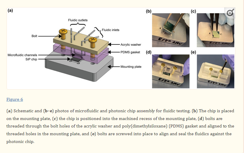
To assemble the setup for fluidic testing (Figure 6), the photonic chip was first placed in the machined recess of the mounting plate. A rectangular washer of the same dimensions as the fluidic gasket and with 4.5 × 2.5 mm rectangular holes aligned with the fluidic I/Os was custom laser-cut from ⅛” acrylic (McMaster-Carr, Elmhurst, IL, USA) using a Universal Laser Systems VersaLaser VLS2.30 laser cutter (Universal Laser Systems, Inc., Scottsdale, AZ, USA). 4–40 brass bolts (McMaster-Carr, Elmhurst, IL, USA) were threaded through the bolt holes in the acrylic washer (first, so that the washer sat against the bolt head) and the PDMS fluidic gasket to align the two pieces together. The bolts were then aligned with the threaded holes in the mounting plate and screwed into place to align and seal the fluidics against the photonic chip. The washer serves to provide even pressure to the flat PDMS gasket to maintain a good seal without a permanent plasma bond between the PDMS and the photonic chip.

2.6. Bulk Sensitivity Testing

Bulk sensitivity measurements were performed by measuring the resonance wavelength shifts of the SWG MRRs during exposure to NaCl (Fisher Scientific S271-3, Thermo Fisher Scientific, Hampton, NH, USA) solutions with five different salt concentrations (0 M, 0.0625 M, 0.125 M, 0.250 M, and 0.375 M) and known refractive indices. The solutions were prepared using ultra-pure water. The refractive indices of the solutions were measured with an Abbe refractometer (Spectronic Instruments, Inc., Rochester, NY, USA). From lowest to highest concentration, the measured refractive indices of the solutions were 1.3335, 1.3341, 1.3346, 1.3360, and 1.3373. It should be noted, however, that these are visible wavelength refractive indices and do not account for chromatic dispersion. 

The photonic chip was assembled with the microfluidic gasket and mounting plate, as described in Section 2.5. To perform the bulk refractive index sensing measurements, the photonic chip assembly was secured on the stage of the custom optical testing setup (Maple Leaf Photonics, Seattle, WA, USA) using thermally conductive tape. A Fluigent LineUp™ series fluid control system (Fluigent, Le Kremlin_Bicêtre, France) was used to supply fluid to the photonic chip assembly. Further details about this setup are provided in Section S2 of the Supplementary Materials.The photonic chip was assembled with the microfluidic gasket and mounting plate, as described in Section 2.5. To perform the bulk refractive index sensing measurements, the photonic chip assembly was secured on the stage of the custom optical testing setup (Maple Leaf Photonics, Seattle, WA, USA) using thermally conductive tape. A Fluigent LineUp™ series fluid control system (Fluigent, Le Kremlin_Bicêtre, France) was used to supply fluid to the photonic chip assembly. Further details about this setup are provided in Section S2 of the Supplementary Materials.

During the experiment, the salt solutions were flowed over the MRR sensor via the two microfluidic channels in sequence at 30 µL/min for 20 minutes each. In the first replicate of the experiment, the salt solutions were flowed over the MRR sensor in order of ascending concentration, starting with water (0 M NaCl), followed by 0.0625 M, 0.125 M, 0.250 M, and lastly 0.375 M NaCl solutions. In the second replicate, the salt solutions were flowed over the MRR sensor in order of descending concentration. This was repeated four more times to reach a total of ten replicates. It is important to note that a known limitation of PDMS is that it can leach uncured oligomers into microchannels, with the oligomer concentration being inversely proportional to the flow rate [89]. Given the relatively high flow rate of 30 µL/min used in this study (corresponding to a residence time of ~2 s in the microchannels), in addition to the considerable precedent for use of PDMS-based microfluidics in SiP assays [3,28,71,90], oligomer leaching was expected to have a negligible effect on the bulk refractive index sensing experiments performed in this work. PDMS is also known to absorb small hydrophobic molecules, with absorption increasing with increasing residence time [91,92]. While not a concern in this study, which only used aqueous salt solutions and short residence times, this would be a relevant consideration in sensing assays using longer residence times and precious, low-concentration, and hydrophobic samples.

During the experiment, a custom Python acquisition script was used to sweep the tunable laser source over a 20 nm wavelength range (1540–1560 nm for the C-band devices and 1290–1310 nm for the O-band devices) and record the output transmission spectra from the photonic chip every 20–30 s. The fiber array alignment was monitored and adjusted every 30 sweeps using a fine align function to ensure good coupling to the on-chip grating couplers throughout the experiment.

Acquired optical spectra were analyzed using a custom Python script to Lorentzian-fit each resonance peak and track the cumulative peak shifts, generating plots and datasets of average resonance peak shift vs. time for each measured microring resonator sensor. Briefly, the custom Python script identified resonance peaks in the optical spectra and fit each resonance peak to a 4-parameter Lorentzian function (x-position of the peak center, height of the peak baseline, height of the peak, and peak width at vertical midpoint). It thus parameterized each resonance peak into a 4-element vector and each optical spectrum with n resonance peaks as an n × 4 matrix. It then matched resonance peaks in consecutively acquired spectra by computing the cosine similarity of the vectors [93], and computed the differential displacement in the x-position of the peak centers of the matched peaks. Finally, it averaged the computed differential displacement of all of the matched resonance peaks in the spectra to calculate the overall differential displacement for that sweep iteration (δλ). The overall resonance peak shift at time point i (Δλ(ti)) was calculated as the sum of all preceding displacements: Δλ(ti)=∑i1δλ.

All resonances demonstrated a gradual blue drift throughout these experiments. Therefore, prior to further analysis, the peak shift data were drift-corrected by performing a linear fit to the baseline of each peak shift plot and subtracting this linear fit from the data. From the resonance peak shift vs. time data, the bulk refractive index sensitivity values were computed using a custom MATLAB script. The MATLAB script plotted the resonance peak shift vs. time data and prompted the user to click on the regions of the plot corresponding resonator response to each bulk refractive index standard saline solution. For each refractive index standard region, the script averaged the resonance peak shift data in a 20-timepoint region (corresponding to approximately 400s of acquisition) centered at the user’s click location. The bulk refractive index difference was computed as the difference between the measured refractive index of each refractive index standard saline solution and that of water. It then performed a linear regression on the peak shift vs. measured bulk refractive index difference (forcing zero intercept), and the slope of the linear regression was taken to be the bulk refractive index sensitivity.

2.6. Bulk Sensitivity Testing
A Zeiss Sigma scanning electron microscope (SEM, Carl Zeiss AG, Jena, Germany) was used to image the fabricated photonic chips. Imaging was carried out to compare the designed dimensions to the fabricated structures and identify any fabrication limitations or unexpected effects. In-lens and secondary electron detectors were used to take top-view and angled-view (45° tilt) images of the photonic devices. ImageJ was used to measure the dimensions of the fabricated SWG waveguides on top-view SEM images taken at 50,000× magnification. For each geometrical parameter (w, Λ, δ, and wfb), five measurements were taken and then averaged to give a more representative estimation.

Results

3.1. Simulation Overestimates In-Water Group Indices of SWG Waveguides

Silicon microring resonators with the waveguide geometries outlined in Table 1 were fabricated on a SOI wafer with no oxide cladding using ANT’s electron-beam lithography process [82]. A circular ring geometry was used for the sensors instead of a racetrack geometry to eliminate mode-mismatch losses [3]. All microrings were designed with a radius, R, of 30 µm, which was selected to ensure low bend losses [3,94]. To characterize the fabricated microring resonators, a tunable laser was coupled to the devices and their transmission spectra were collected while sweeping the wavelength of the input laser from 1530–1560 nm for the C-band devices or 1270–1310 nm for the O-band devices. This characterization was performed with a droplet of water fully covering the regions of the chip containing the resonators. The measurements were performed on five replicate chips and the measured spectra were analyzed using a custom script, as described in Section 2.4.

Table 2 reports the simulated and measured group indices and FSRs of the fabricated ring resonators. All measured group indices were lower than those predicted by simulations, with the boneless SWG devices generally exhibiting a slightly greater difference in ng between the measured and simulated values compared with the fishbone devices. Accordingly, the measured FSRs were greater than the simulated values for all geometries.

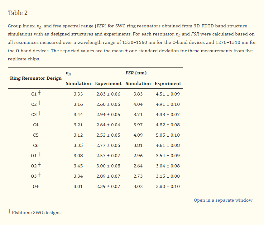
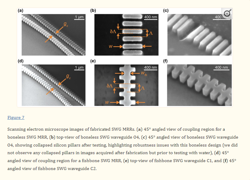
Our group has previously fabricated boneless SWG microring resonators using the identical geometry as design C6 from this work, using a different electron-beam lithography fabrication process [19]. Previously, 30 µm-radius ring resonators fabricated with this waveguide geometry (Λ = 250 nm, δ = 0.7, w = 500 nm, t = 220 nm) exhibited an experimental ng of 3.27 and FSR of 3.936 nm, which align well with the simulated values reported here. This indicates that simulation inaccuracies are unlikely to be the source of variation in ng and FSR between the simulated and measured results. Instead, these variations are likely attributable to experimental factors, such as differences between the designed and fabricated structures. In particular, we hypothesized that the low experimental group indices may be due to smaller-than-designed feature sizes on the fabricated chips. To test this hypothesis, SEM imaging was performed on the fabricated structures and feature sizes were measured. The SEM imaging highlighted two unexpected observations regarding the fabricated waveguide morphologies. First, regarding fabrication tolerances, most waveguide features were slightly smaller than designed. Typically, w was 18–25 nm smaller than designed, wfb was 0–11 nm smaller than designed, and δ was approximately equal to the designs. Corners were slightly rounded, though this effect was small. Second, boneless SWG design O4, which had the smallest silicon pillars out of the fabricated devices, showed many collapsed pillars, as seen in Figure 7c. Stiction is known to cause damage to features on micro- and nanoscale devices when exposed to liquid, then dried [58]. Capillary forces pull the feature toward the substrate or adjacent features during this process, leading to deformation, and inhibiting reuse of the device [57,58,59].

The SEM-imaged chip shown in Figure 7 had been exposed to water for characterization prior to imaging, meaning stiction is a likely cause of the visualized damage. Subsequent SEM imaging of an unused chip suggested that this damage was not present before exposure to liquid. This type of damage was not observed for any other waveguides, including design O3, which had the same geometry as O4, but with the addition of a 100 nm fishbone, highlighting the additional structural stability conferred by the fishbone. Drying SiP chips in a low-surface tension solvent (e.g., pentane) is one strategy employed by foundries to prevent stiction during the fabrication process [59,95]. In many applications, however, this may not be feasible due to incompatibilities between these solvents and microfluidic materials [58]. Additionally, the chemical processes used to functionalize SiP sensors for biosensing often involve aqueous solutions and expose the chip to multiple cycles of wetting and drying [96]. In these applications, fishbone SWGs can reduce the risk of damage prior to biosensing assays.

To assess the effect of fabrication tolerance on device performance and determine if the low experimental group indices could be attributed to the smaller-than-designed feature sizes observed in the SEM images, we re-ran band structure simulations for designs C1 and C4, this time using their measured geometries. The smoothing of corners was not included in these simulations due to the small magnitude of this effect, as observed in SEM images. However, this corner smoothing should be accounted for in simulation models of waveguides fabricated with photolithography techniques (e.g., Deep UV lithography), which are known to cause prominent corner smoothing [83]. The group indices obtained from these simulations were 3.108 and 3.110, respectively, which represent a ~3–7% reduction in ng compared with the original simulations, but not a sufficiently large reduction to completely account for the experimental results.

Another possible explanation for the low experimental group indices is incomplete wetting of the SWG structures. Nanostructured surfaces can be susceptible to this phenomenon, which leads to the entrapment of air between narrow features during wetting [97]. As such, air may have been trapped between the silicon pillars when the photonic chips were coated with water for measurements. Because air has a lower refractive index than water, this is expected to decrease neff [50]. The group index can be related to neff according to ng(λ)=neff(λ)−λ⋅(dneff/dλ) [74], where dneff/dλ<0 for the designed waveguides. While the first term of this equation should decrease in the case of incomplete wetting, the magnitude of the second term should also decrease when air is added to the SWG metamaterial, as air is less dispersive than water [77]. Depending on the relative effect of trapped air on these two terms, incomplete wetting may cause a decrease in ng. To theoretically test this hypothesis, simulations were performed with fishbone SWG design C1 in which the gaps between the silicon pillars were filled with air up to a height tair (Figure S2). The fabricated waveguide geometry, as measured from SEM images, was used. Further details regarding these simulations are provided in the Supplementary Materials (Section S3). These simulations showed that the combination of reduced feature sizes and air entrapment considerably reduced ng and an increase in tair led to a decrease in ng (Figure S3). An air pocket height of tair = 120 nm yielded ng = 2.825, which is very close to the experimentally measured value of ng = 2.83. It should be noted that this model does not account for the curvature of the air–water interfaces enclosing the air pocket. Regardless, these simulation results suggest that the low experimental ng values may, indeed, be the result of incomplete wetting. Similarly to stiction during drying, incomplete wetting can cause deformations and damage to structures adjacent to the trapped air due to capillary pressure [97]. This may have contributed to the feature collapse seen in Figure 7c. Another similar phenomenon that may have contributed to the low group indices is nanobubble formation on the waveguide surfaces due to etch roughness [98]. The presence of a thin native oxide layer on the waveguide surface is yet another factor that may have contributed to these results [99].

3.2. Empirical Characterization of Extinction Ratio vs. Coupling Gap Reveals Insights for Further Optimization and Highlights Performance Degradation Due to Peak Splitting

Critical coupling is achieved when the coupling gap, gc, between the bus waveguide and ring resonator is such that the power coupled into a ring resonator is equal to the round-trip losses in the ring [20]. At critical coupling, the extinction ratios (ERs) of the resonance peaks are maximized, thus enhancing the signal-to-noise ratio; this is a desirable condition for robust peak tracking and sensitive analyte detection [98]. When gc is relatively small, the resonator is over-coupled, giving rise to increased power losses. This decreases both ER and Q. When gc is relatively large, the resonator is under-coupled, which increases Q, but decreases ER. Indeed, under-coupling can be used to enhance iLoD, although a tradeoff with ER exists for noisy systems that necessitate higher ERs for robust peak tracking [100]. In this work, we aimed to optimize ER to facilitate straightforward extraction of the sensor intrinsic quality factor for comparison with propagation loss simulations, as well as facilitate meaningful comparison to previously reported sensors operating near critical coupling [3,21,28]. Subsequent system design (building upon the optimization framework presented here) should consider the tradeoff between Q and ER in choosing the best coupling condition for the application, and may choose to under-couple the resonators.

To achieve critical coupling, gc can be selected based on numerical simulations. For example, the critical coupling condition can be estimated based on simulated coupling coefficients extracted from FDTD simulations of the entire coupling region, along with simulated propagation losses [20,101]. However, one drawback of this approach is that FDTD simulations of the coupling region are very computationally intensive for SWG resonators. Additionally, while these FDTD coupling coefficient and loss simulations account for loss contributions due to material absorption and substrate leakage, they often do not accurately recapitulate the effects of optical scattering, which depend on the surface roughness of the fabricated waveguides and can increase losses and affect the coupling condition [20]. Scattering has an increased effect on SWG waveguides compared to conventional strip waveguides owing to the increased surface area of SWG structures [3,39]. Considering these limitations, we decided to take an empirical approach to optimize gc for close-to-critical coupling. 
Each resonator was fabricated with four different coupling gaps. The fabricated coupling gaps for the C-band devices were based on our group’s previous empirical findings for conventional SWG ring resonators with similar expected effective indices. As outlined in Table 1, coupling gaps of gc = 450, 500, 550, and 600 nm were fabricated for devices C1, C2, C4, and C5, which had simulated effective indices between 1.70–1.71. Smaller coupling gaps of gc = 400, 450, 500, and 550 nm were selected for C3 and C6 due to their greater predicted effective indices and, therefore, increased optical confinement. It has been reported that coupling increases with increasing wavelengths due to reduced optical confinement at the defined waveguide geometry of w = 500 nm and t = 220 nm [20]. As such, smaller coupling gaps were selected for the O-band devices, relative to their predicted effective indices. Coupling gaps of gc = 400, 450, 500, and 550 nm were fabricated for O1 and O4, whereas coupling gaps of gc = 350, 400, 450, and 500 nm were fabricated for O2 and O3 due to their higher simulated effective indices.

The extinction ratios for all resonator designs were measured, as described in Section 2.4, and the results are presented in Figure 8 and Table 3. This characterization was performed for five replicate chips and mean values are reported. Details regarding the number of resonance peaks included from each chip in each mean calculation are provided in Section S4, Table S1. As shown in Figure 8b, all C-band devices, excluding C3, exhibited maximum extinction ratios at their largest coupling gaps. Consequently, it cannot be concluded that critical coupling was achieved for these devices, and future work should include the fabrication of these resonators with larger coupling gaps to avoid over coupling. In SEM images, the measured coupling gaps were 20–40 nm smaller than designed, which may be related to proximity effect correction in the lithography process [102]. This may have contributed to this requirement for larger coupling gaps. As illustrated in Figure 8c, devices O1, O2 and O3 exhibited maximum extinction ratios at intermediate values of gc within their fabricated ranges. However, the variations in extinction ratio between different values of gc are similar in magnitude to the standard deviations of the measurements, so these results may not confirm critical coupling. Resonator O4 achieved an extinction ratio at its largest fabricated coupling gap, further highlighting that future work should extend the coupling gap ranges investigated here.

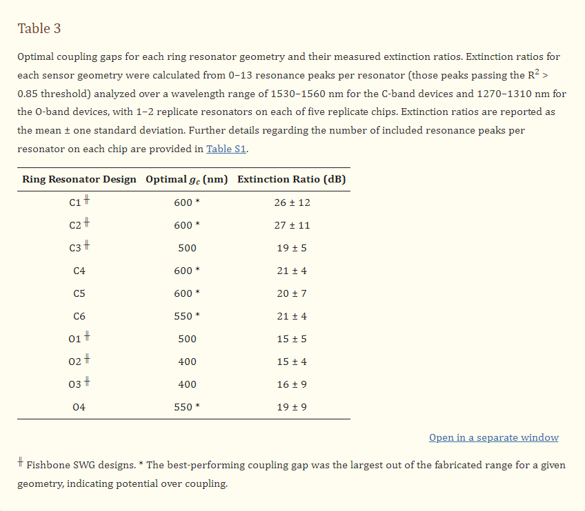
Variations in maximum extinction ratios between the devices, in particular between the C-band and O-band devices, may be attributable to peak splitting. Peak splitting was visible in the resonator spectra and was particularly prominent for the O-band devices. This peak splitting, which is discussed further in the next section, leads to deleterious effects on the resonator performance, including a reduction in peak height, potentially explaining why the maximum extinction ratios measured for the O-band resonators were lower than those measured for the C-band resonators [103,104]. Peak splitting largely arises due to stochastic scattering effects, which vary with wavelength [20]. This can lead to unpredictability in peak splitting severity between resonances, which may account for the large standard deviations of the measured extinction ratios [20]. This peak splitting may also be responsible for the absence of prominent maxima for devices O1, O2 and O3 in Figure 8c. As the measurements were made over wavelength ranges of 30–40 nm, it is likely that the wavelength-dependence of coupling within these wavelength ranges also contributed to the large standard deviations [20]. Finally, the detectors used in the experimental characterization of the sensors had a minimum detectable power of −80 dBm, which meant that some high-extinction ratio peaks were clipped at their minima. This may have added to the large standard deviations and may have caused an underestimation of some extinction ratios for designs close to critical coupling.

3.3. Fishbone SWG MRRs Achieve Comparable Performance to Previously Reported SWG-Based Sensors

Quality factors were estimated for all fabricated resonator designs by simulating the waveguide propagation losses, as described in Section 2.1.2, then calculating the critically coupled quality factor, according to Equation (4). The simulated losses and corresponding quality factors for all waveguide designs are presented in Table 4. Indeed, these simulated losses and quality factors do not account for the effects of fabrication-related optical losses, but they do provide the fundamental limit for the device performance [3]. This offers a valuable benchmark against which to compare experimental results, which can help to identify the contribution of fabrication-related losses to the real device performance and inform future approaches to mitigate these effects.

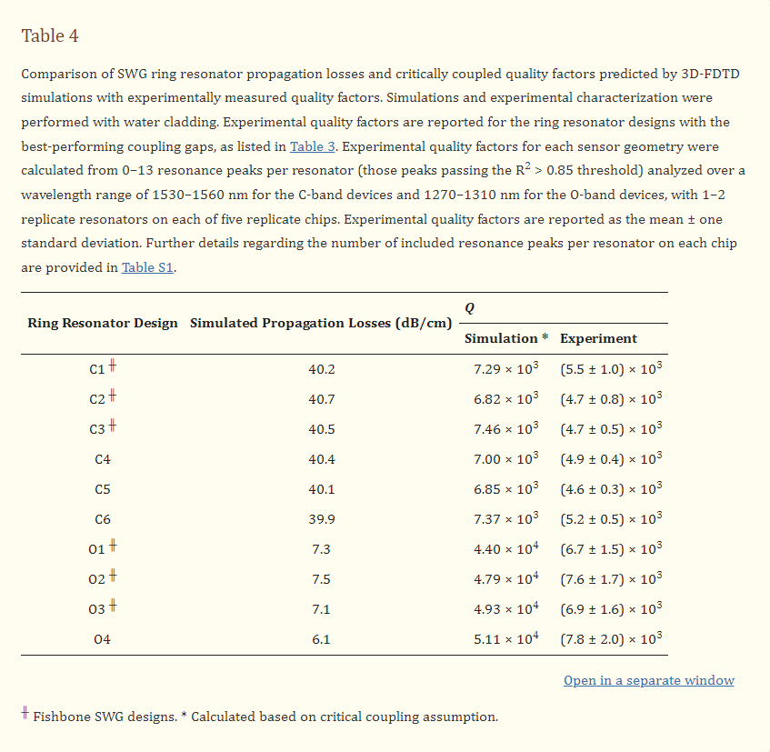
Optical absorption in water is the dominant loss mechanism for waveguides operating in the C-band. Since the predicted effective indices were similar for all of the fabricated C-band designs, indicating similar modal confinement, similar losses were expected among these devices [3]. The simulated losses aligned well with this, as all simulated losses were between 39.9–40.7 dB/cm, suggesting that wfb and δ have little effect on the material losses of SWG waveguides with similar effective indices.

It has been reported that the optical absorption of water is roughly ten times lower in the O-band than the C-band, allowing for significantly lower material losses [3,21]. This is reflected in the simulated propagation losses for the O-band structures, which ranged from 6.1–7.5 dB/cm. These losses are roughly six times lower than the C-band propagation losses, which is a smaller reduction in losses compared to what would be predicted if the losses were solely due to material absorption. This discrepancy may be due to small losses to the substrate and PML boundaries. Corresponding to their lower losses, the simulated quality factors for the O-band resonators were considerably greater than those for the C-band resonators, highlighting the potential benefit of using the O-band light for sensing applications.

Quality factors for the fabricated ring resonators were calculated from the measured spectra, as described in Section 2.4, and the results are provided in Table 4. For the C-band devices, the simulated quality factors were 1.3–1.6 times as large as the experimental values. This difference between simulated and experimental values is likely due to scattering and coupling losses, which were not accounted for in the simulations. Scattering losses arise due to roughness introduced on the waveguide surfaces during fabrication, which makes them challenging to model. These losses are typically non-negligible for SWG waveguides owing to their large surface area [3,94]. Next, overcoupling leads to greater optical losses compared to critical coupling [100]. As discussed in the previous section, many of the C-band resonators were likely overcoupled, giving rise to this loss mechanism. Since the simulated quality factors were calculated based on the critical coupling assumption, these losses are another likely source of variation between the simulated and experimental results. It should be noted that the propagation loss simulations described in this work also did not include bending losses. Based on previously reported results, we expected negligible bending losses at the large ring radius of 30 µm considered here [3].

The simulated quality factors for the O-band resonators ranged from 4.40 × 10⁴ to 5.11 × 10⁴, whereas the experimentally measured values were 6.3–7.2 times lower (Table 4). While scattering and coupling losses, combined with the smaller-than-designed feature sizes of the fabricated structures, likely contributed to this discrepancy, peak splitting appeared to be the dominant source of this variation. In an ideal ring resonator, there exist two counterpropagating circulating modes, clockwise and counterclockwise, which are uncoupled, and degenerate, meaning they resonate at the same frequency [104,105]. In this case, the resonator exhibits single peaks. A small mode perturbation, however, can couple these modes and break their degeneracy leading to a resonance shift that manifests as split resonance peaks [20,103,104]. In silicon waveguides, this perturbation typically occurs due to stochastic backscattering arising from sidewall roughness [20,103,104]. In the spectra measured for all O-band resonators, peak splitting was prevalent, comprising 18–51% of all resonances. Conversely, split peaks were far less common in the C-band resonator spectra, comprising roughly 2–12% of all resonances. While all resonators studied in this work were fabricated using the same foundry process and, therefore, were subject to similar sidewall corrugations, the exaggerated peak splitting observed among the O-band devices suggests that sidewall scattering is exacerbated at lower wavelengths. This is consistent with analytical models for scattering losses in which the losses are proportional to the square of the ratio of surface roughness to the wavelength of light in the material [106]. Thus, the effects of scattering, and therefore, peak splitting, increase with decreasing wavelength. Additionally, the higher water absorption at 1550 nm may be hiding peak splitting, whereas a 10× lower water absorption at 1310 nm would reveal scattering induced peak splitting.

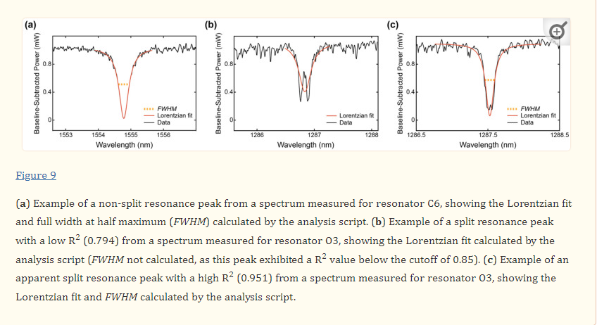
The analysis script used to extract the quality factors from the measured spectra performed Lorentzian fitting on the resonance peaks to measure the FWHM, from which the quality factors were calculated. In the case of split peaks, the Lorentzian was typically fit to the doublet, leading to an underestimation of Q (Figure 9). In this analysis, a R2 cutoff of 0.85 dictated which peaks were used in the calculation of Q. The split peaks typically exhibited poor R2 values compared with single peaks (Figure 9b); however, there was considerable overlap, with some apparent split peaks exhibiting higher R2 values than some single peaks (Figure 9c). However, it should be noted that some peaks, such as the one shown in Figure 9c, exhibited apparent peak splitting that had a similar magnitude to the spectral noise, making it challenging to confidently confirm the identity of these peaks as split or non-split.

To test whether increasing the selection stringency effectively eliminated split peaks from the quality factor calculation, the analysis was repeated on the O-band data with the R2 threshold increased to 0.95. This analysis did not produce a noticeable difference in the results and incompletely filtered out the split peaks, while eliminating numerous single peaks and underestimating the quality factors. While it may be possible to perform improved fitting to the doublets to extract more accurate quality factors in post processing, their extinction ratios will still be degraded. Further improvements could be made to the analysis algorithm to filter out split peaks and only analyze apparent non-split peaks, but such an approach is confounded by the variable severity of the split peaks. For example, split peaks may be visually imperceptible in cases where the splitting is less than a linewidth, yet these peaks will still exhibit degraded extinction ratios and quality factors. As illustrated in Figure 9c, when the magnitude of peak splitting is similar to the noise in a given spectrum, it may also be challenging to confirm the identity of split peaks with high confidence. Overall, the prevalence of these split peaks is likely to cause deleterious effects in the analysis of binding assays.

Therefore, a more robust solution for improving sensor performance is to design resonators that are less sensitive to backscattering. The back reflections that cause peak splitting have been reported to increase with ng [20]. This is consistent with our experimental results. Resonator design O4, which had the lowest ng out of the O-band devices, demonstrated the least peak splitting, with split peaks comprising approximately 18% of all resonances measured across five chips. Resonator designs O2 and O3, which had the two highest values of ng, demonstrated the most peak splitting, at roughly 50% and 51% of all resonances, respectively. In these estimates, it should be noted that split peaks with very low extinction ratios (e.g., due to overcoupling) were nearly indistinguishable from noise. This meant that some split peaks may have been overlooked, resulting in an underestimation of their true occurrence. Among the resonators that had sufficiently high extinction ratios to confirm the identity of split peaks, O1, O2, O3, and O4 exhibited peak splitting on approximately 42%, 54%, 70%, and 27% of their resonances, respectively. Overall, these data suggest that reducing ng by reducing δ and/or wfb may improve the resonator performance. This should be accompanied by a detailed analysis of O-band substrate leakage losses to ensure that any feature size reductions do not introduce additional deleterious effects. Finally, electron-beam fabrication processes have been found to yield semi-periodic surface roughness [20]. If the surface roughness of the fabrication process is well-characterized, simulation models can be established to better predict the extent of backscattering at different wavelengths, which may help predict peak splitting and inform ring resonator design [20]. If possible, a reduction in etch roughness could further reduce these scattering effects. Fishbone SWG structures fabricated by Deep UV lithography are likely to have reduced sidewall roughness. In electron beam lithography processes similar to that used in this work, the shot pitch and machine grid are very small (e.g., 5–6 nm) and the electron beam size is roughly 10–20 nm [83]. The quantization of shots, which are not very well smoothed out by the small beam size, to the machine grid results in high-resolution roughness. In contrast, Deep UV lithography processes use masks made by electron beam lithography, but they are smoothed out by the 193 nm wavelength of light used for the exposure and pattern transfer [83]. Hence, peak splitting is expected to be reduced for devices fabricated by 300 mm wafer 193 nm immersion Deep UV lithography foundries. Moreover, Deep UV lithography processes now enable high-volume manufacturing of SiP chips with sub-100 nm feature sizes, making Deep UV lithography an attractive option for mass production of SWG-based sensor chips [42,83,107].

Next, ring resonator performance was assessed in terms of Sb. The simulated Sb values for all fabricated devices are reported in Table 5. To experimentally measure the bulk sensitivities of the fabricated devices, the sensor chips were interfaced with a two-channel PDMS microfluidic gasket and five NaCl solutions with different concentrations (0–0.375 M) were flowed over the sensors in alternating ascending and descending sequences for a total of ten replicate exposures to each solution. Throughout the experiment, the transmission spectra were measured using a tunable laser and optical detectors. The measurement setup used for these experiments is shown in Figure 10a. For each resonator design (C1–C6 and O1–O4), two replicate resonators were monitored, one of which was located in microfluidic channel 1 and the other in channel 2. The same fluid sequence was delivered to both microfluidic channels. On the chip layout, the C-band and O-band devices were accessible from grating couplers on opposite edges of the 9 mm × 9 mm photonic chip. This meant that the microfluidic gasket had to be rotated 180° to access the C-band devices compared to the O-band. When the gasket was aligned to the C-band devices, the O-band resonators were in direct contact with PDMS, and vice versa. As the chips were fabricated without an oxide cladding, this made the resonators in direct contact with the PDMS prone to damage during gasket alignment and removal. Therefore, the C-band and O-band devices were tested with microfluidics on separate chips to prevent damage to the resonators prior to use. The resonators’ saved spectra were analyzed by a custom retrospective analysis script to track the resonance wavelength shifts of the sensors, as described in Section 2.6. An example of a spectrogram collected during one of these experiments and an overlaid peak shift plot generated by the retrospective analysis script are shown in Figure 10b. An example of the spectral peak shifts corresponding to each salt solution is shown in Figure 10c.

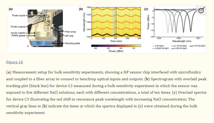
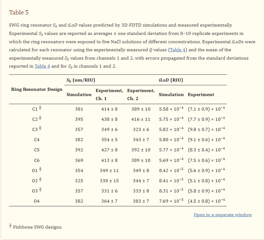
The peak shift plots all demonstrated a gradual baseline blue drift over time (10–72 pm/hr). While the source of this drift is unclear, one contributor may be the gradual etching of silicon by NaCl solution [108]. Prior to further analysis, the peak shift data were, therefore, drift-corrected by performing a linear fit to the baseline of each peak shift plot and subtracting this linear fit from the data. Sb was then calculated by performing a linear regression on the resonance peak shifts versus the bulk refractive index of the salt solutions data, and extracting the slope, as illustrated in Figure 11. For each resonator, Sb was calculated as the average slope from 8–10 linear regressions (on the data from 8–10 replicate exposures to all five salt solutions), and the average values and their standard deviations are presented in Table 5. It should be noted that only eight replicates were used when peak shift abnormalities, such as abrupt jumps and drops (likely due to bubbles passing through the fluidic system), were observed during the first replicate. In these cases, the first two replicates were excluded from the calculated averages to maintain an equal number of ascending- and descending-concentration replicates.

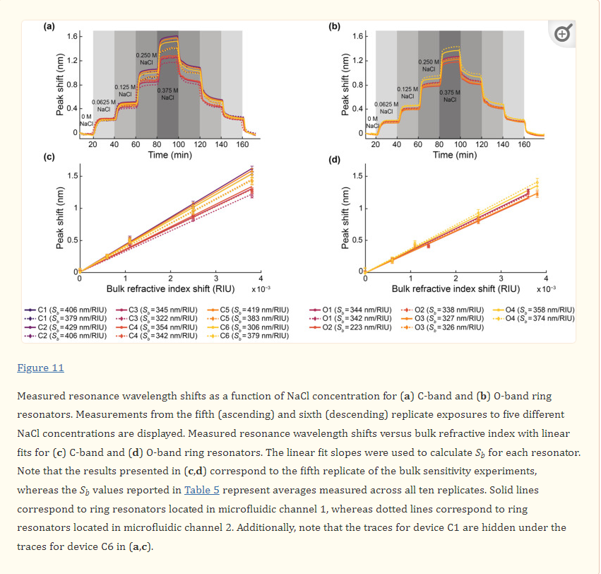
On average, the experimental results aligned well with the simulated ones, but the experimental results showed variations in bulk sensitivity between the two microfluidic channels. For the C-band designs, resonators in channel 1 always demonstrated higher values of Sb, whereas for the O-band designs, excluding O1, resonators in channel 2 always demonstrated higher values of Sb. For O1, Sb was virtually identical between the two channels. This spatial variation in Sb is illustrated in Figure 12a. These variations similarly affected the fishbone and boneless structures. To determine if this variation was the result of variability among the fabricated resonator structures, the spatial variation of ng was similarly analyzed based on the results obtained in Section 3.1 (Figure 12b), which showed that ng did not vary as a function of location on the chip for replicate resonator designs, though the boneless devices typically exhibited larger differences between the experimental and simulated group indices compared to the fishbone structures. This suggests that experimental factors related to fluidics were the most likely source of variation in Sb.

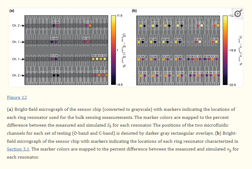
In these experiments, the NaCl solutions used in both channels were aliquots of the same stock solution, eliminating the solutions as a source of error. Further, the fluid control system was programmed to deliver identical flow rates through both channels. These flow rates were monitored by flow sensors throughout the experiments to ensure that the expected flow rates were delivered, making this another unlikely source of error. The refractive indices of the NaCl solutions used in the Sb calculations were measured with an Abbe refractometer at visible wavelengths and chromatic dispersion was not accounted for, which could constitute one source of experimental error.

The presence of trapped air between the silicon pillars of the SWG waveguides due to incomplete wetting may be responsible for the variations in Sb. Firstly, as discussed in Section 3.1, this phenomenon may have contributed to the lower-than-predicted values of ng. Sb is inversely proportional to ng, so a decrease in ng may lead to an increase in Sb. However, this cannot be decoupled from variations in the susceptibility, which may also arise as a result of trapped air. Trapped air in the gaps between the silicon pillars could reduce the interaction between the evanescent field and bulk fluid in these regions of high electric field intensity, reducing susceptibility. Conversely, the decrease in modal confinement associated with the decrease in neff may increase modal overlap with the bulk, potentially increasing susceptibility. Thus, the effects of this phenomenon on ng, susceptibility, and therefore Sb, are challenging to predict and may account for some of the variability observed here. Supplementary Materials Section S3 presents simulation results for a model of incomplete wetting for waveguide design C1. As shown in Figure S3, an increase in the height of the trapped air pockets between the SWG pillars decreased Sb. It is possible that differences in the speed at which fluid was introduced to the microfluidic channels affected the extent of wetting and the average sizes of these air pockets. This could have contributed to the differences in Sb between the channels. However, based on the simulation results, these differences in Sb should correlate to differences in ng between the channels. This was not observed experimentally (Figure S5). Nevertheless, the simulation model does not account for the shape of the air pocket, which may also influence Sb, potentially explaining these differences. Lastly, it should also be noted that the simulation results provided in Section S3 generally predict lower values of Sb compared with the experimental results. These simulated values were obtained at a single wavelength (1550 nm), whereas the experimental measurements were obtained from multiple resonances analyzed over a wavelength range of 1530–1560nm, which likely contributed to these discrepancies between the experiments and simulations.

Overall, the fishbone SWG resonators achieved comparable, and sometimes better, sensitivities than the boneless SWG designs. For the C-band resonators, fishbone device C2 achieved, on average, the greatest bulk sensitivity at 438 and 416 nm/RIU in channels 1 and 2, respectively. For the O-band resonators, boneless SWG design O4 achieved the greatest bulk sensitivity at 364 and 383 nm/RIU in channels 1 and 2, respectively. However, these values only surpassed the best-performing O-band fishbone resonator (O1) by 15 and 34 nm/RIU in channels 1 and 2, respectively.

Figure 13 compares the reported performance of SWG resonators based on quality factor, Sb, and iLoD. TE and TM strip waveguide resonators are also included as performance benchmarks. Lines of constant iLoD are plotted, showing that iLoD decreases and resonator performance improves toward the top right corner of the plot. The C-band and O-band boneless SWG (C6 and O4) and fishbone SWG (C1 and O2) resonators that demonstrated the smallest experimental values of iLoD in this work (listed in Table 5) are also included on the plot. The plotted bulk sensitivities for these devices are averages from the two microfluidic channels. It should be highlighted that several of the resonators with the highest iLoDs on this plot have been characterized based on simulations with gaseous cladding material (legend entries marked with a section sign, §) [54,55]. These reported levels of performance are likely considerably greater than what can be achieved with the same sensor architectures applied to real-world aqueous-phase sensing due to the additional material and scattering losses. All other sensor performance data are based on experimental results measured with water cladding.

4. Conclusions

In this work, we demonstrated the optimization and experimental characterization of SiP MRR sensors designed with fishbone SWG waveguides for both O-band and C-band operation. Waveguide designs were optimized based on 3D-FDTD simulations to find combinations of Λ, δ, and wfb that optimize sensitivity while meeting the substrate leakage loss criterion. MRRs were fabricated with the optimized waveguide designs and experimentally tested to evaluate their optical properties, spectral characteristics, and performance compared to boneless SWG MRRs in terms of ng, FSR, extinction ratio, Q, Sb, and iLoD. The O-band fishbone SWG MRRs achieved quality factors as high as 7.8 × 10³, bulk sensitivities as high as 349 nm/RIU, and intrinsic limits of detection as low as 5.1 × 10⁻⁴ RIU. The C-band fishbone SWG MRRs achieved quality factors as high as 5.5 × 10³, bulk sensitivities as high as 438 nm/RIU, and intrinsic limits of detection as low as 7.1 × 10⁻⁴ RIU. In general, the fishbone SWG resonators presented in this work have comparable performance to other SWG sensors that have been experimentally demonstrated to date, while offering improved fabricability and a lower risk of damage compared with the boneless designs. The performance of the O-band resonators was, however, hindered by peak splitting. This peak splitting was likely the result of scattering effects, which were exaggerated at lower wavelengths and likely exacerbated by fabrication issues. These scattering effects could be reduced by designing waveguides with lower group indices and designing models to better predict the effects of etch roughness. This highlights the potential to realize O-band fishbone SWG MRRs with higher quality factors and lower limits of detection than current state-of-the art SWG sensors. One of the challenges with SWG structures is the small feature size required in fabrication. O-band, as opposed to C-band, involves slightly smaller features, which in this paper were a minimum size of 100 nm, and a minimum gap of 100 nm. These sizes are compatible with deep immersion 193 nm CMOS foundry fabrication, hence can be fabricated in high volume. Overall, the results of this work indicate that fishbone SWG waveguides allow for improved robustness and fabricability without compromising performance. While we have developed a framework for optimizing fishbone SWG MRRs and have experimentally demonstrated their sensing capabilities, the POC use of these transducers relies on system-level integration with other biosensor components. Sensor biofunctionalization, sample delivery, and signal readout strategies must all be optimized for the POC setting in order to successfully translate these SiP devices into fully portable diagnostic tools.

A Low-Cost Microfluidic Method for Microplastics Identification: Towards Continuous Recognition

A Low-Cost Microfluidic Method for Microplastics Identification: Towards Continuous Recognition

Pedro Mesquita, Liyuan Gong and Yang Lin

Abstract Plastic pollution has emerged as a growing concern worldwide. In particular, the most abundant plastic debris, microplastics, has necessitated the development of rapid and effective identification methods to track down the stages and evidence of the pollution. In this paper, we combine low-cost plastic staining technologies using Nile Red with the continuous feature offered by microfluidics to propose a low-cost 3D printed device for the identification of microplastics. It is observed that the microfluidic devices indicate comparable staining and identification performance compared to conventional Nile Red staining processes while offering the advantages of continuous recognition for long-term environmental monitoring. The results also show that concentration, temperature, and residency time possess strong effects on the identification performance. Finally, various microplastics have been applied to further demonstrate the effectiveness of the proposed devices. It is found that, among different types of microplastics, non-spherical microplastics show the maximal fluorescence level. Meanwhile, natural fibers indicate better staining quality when compared to synthetic ones.

Key words:  microfluidics; microplastics; continuous identification; low-cost; 3D printing

We kindly thank the researchers at University of Rhode Island for this collaboration, and for sharing the results obtained with their system.

Introduction

It has been estimated that the ongoing COVID-19 pandemic has exceedingly increased the demand for the use of plastics [1]. As of 23 August 2021, more than 8.4 million tons of pandemic-associated plastic debris were released into the oceans [2]. Among them, most of the plastic debris was microplastics with a size smaller than 5 mm [3,4], and this can be classified into primary and secondary microplastics. Generally, primary microplastics are the microscopic plastics that were intentionally made small (e.g., microbeads used in cosmetics) [5,6,7], while secondary microplastics are particles resulting from the breakdown of macroscopic pieces due to the conjoint environmental effects (i.e., photo-oxidation, hydrolysis, microorganism degradation, mechanical shear, etc.) [8,9]. Despite the fact that a variety of plastic types have been identified in microplastics, most of the microplastics in seawater originate from packaging materials (e.g., polyethylene, and polypropylene) [10]. Owing to their small density, these microplastics tend to float on the surface of the water, thus they can spread worldwide (in opposition to denser plastics that tend to settle down) and are more difficult to remove [11,12].

Nevertheless, the current understanding of plastic pollution in terms of the quantity, type, lifetime, and associated health effects largely remains unknown. As a result, microplastic separation and identification serve as an important approach to providing evidence and metrics of the pressing environmental issues caused by plastic pollution [13]. For example, worldwide microplastic assessment is possible to identify hot pollution spots and determine the historical trends which may lead to novel strategies for fighting debris spread [14,15,16]. At present, quite a few identification techniques have been explored for microplastic identification. Among them, common methods include visual inspection, Fourier-transform infrared spectroscopy (FTIR), Raman spectroscopy and scanning electron microscopy (SEM) [17,18]. Despite their effectiveness, these techniques, except visual inspection, rely on expensive apparatus and time-consuming detection methods that are limited to trained personnel, thus hindering the expansion of these methods for high-throughput detection [19,20,21].

As a result, visual inspection, though not as effective as other sophisticated counterparts, is still widely applied for faster recognition [22,23]. Currently, a variety of sampling and identification technologies have been used to improve the performance of visual inspection, of which a commonly used one is the combination of filtration and staining [24,25]. However, filtration often leads to false positives due to potential interference from organic matters in the samples [26,27]. More importantly, its performance is highly reliant on the size of the filters, thus limiting its capabilities in sampling small microplastics. In addition, particles are also prone to adhere to the filters, resulting in ineffective separation of the microplastics for identification [28,29]. In addition, staining of the microplastics relies on staining agents that turn microplastics into prominently visible particles [30,31]. Currently, it is unsurprising that quite a few staining agents (e.g., Rhodamine B, Rose Bengal, Trypan Blue, etc.) have been explored for this purpose. Among them, Nile Red is a hydrophobic fluorophore and was reported to be one of the most effective agents due to its favorable binding performance with lipophilic substances [30,32,33].

Nevertheless, the focus of current studies on microplastic staining and identification has been largely given to batch-by-batch or case-by-case analysis [25,34,35,36]. Therefore, sample collection is still inevitable and remains a time-consuming step in the whole sampling process. Moreover, temporal information is hardly achievable. Given the need of acquiring in-depth studies of microplastic pollution in oceans and other water bodies, long-term monitoring or continuous monitoring is essential and a low-cost, simple and effective method should be developed. Thanks to the burgeoning developments of microfluidic technologies over the past decade, microfluidic devices can be a promising solution to address this need due to their powerful particle control capabilities and the ease of integration in modern electronic systems [37,38]. For example, microfluidics has been used for long-term monitoring of algae in the past [39]. Tumor responses to hypoxia conditions were also analyzed continuously in a microfluidic platform [40]. Indeed, microplastic identification is also not a new research area for microfluidics [41,42], yet to the best knowledge of the authors, microfluidics has not been applied for long-term microplastics assessment and we believe the combination of low-cost Nile Red staining and microfluidic fluid control would provide a novel venue to confront the ever-deteriorating plastic issues without complicated analysis and costly instrumentations. Low-cost fabrication methods such as 3D printing and molding can be applied to further minimize the cost associated with this method, and the miniaturized devices may also be integrated into the monitoring stations near seashores, along with data collection of other water quality metrics on a continuous basis.

Herein, we further explored the staining capabilities of Nile Red through a microfluidic device capable of continuously staining microplastics for rapid identification. The proposed device has two inlets for respective Nile Red and sample injection (Figure 1A), and a serpentine channel that allows for sufficient mixing of the staining agent and the sample. In this paper, we studied the effects of dominating parameters on the identification performance, including Nile Red concentration, temperature, and residency time. Note that prior to performing microfluidic studies, static studies that resemble traditional Nile Red staining processes were adopted and served as a baseline for comparison.

2. Materials and Methods

In this paper, the process of static microplastic identification using Nile Red was carried out without a filter. Specifically, the staining Nile Red solution was added directly into an Eppendorf tube containing the microplastics sample and placed inside an oven (Figure 1B). On the other hand, microfluidic experiments followed a similar procedure: mixing Nile Red and microplastics in the device (which was placed inside an oven). Since the mixing process is passively induced without human operation, this process holds promise for continuous staining.

2.1. Nile Red Preparation
The staining solution was prepared by dissolving Nile Red (technical grade, N3013, Sigma-Aldrich, St. Louis, MO, USA) in methanol to different concentrations. We have considered the limit of solubility of Nile Red in methanol (1 mg/mL) to be the stock solution for further dilution, from which the solution was diluted into 50X, 100X, 250X, 500X, and 1000X samples.

2.2. Microplastics Sample Preparation
 In this paper, lab-prepared and commercially available microplastics were adopted in lieu of naturally formed microplastics. More specifically, microspheres made of polyethylene (PE), ranging from 10–45 µm (Cospheric, Inc., Santa Barbara, CA, USA) were applied to determine the optimal parameters for staining. Other plastics including the microspheres made of polystyrene (PS) with sizes from 9.5–11.5 µm (Cospheric, Inc., Santa Barbara, CA, USA), cotton and acrylic fabric acquired from clothing, polypropylene (PP) and non-spherical PE prepared from plastic storage containers were also applied to test the versability of the proposed method. All the samples were mixed with deionized (DI) water prior to staining. Note that commercial microspheres were diluted in a concentration of 10 mg/mL, while the other samples were diluted to 1 mg/mL, which is because the commercial particles were more available than the ones obtained from other sources.

2.3. Static Experiments
To prepare the samples for static experiments, 100 µL of Nile Red solution was thoroughly mixed with 100 µL of PE microplastic solution inside an Eppendorf tube, followed by baking inside an oven (Quincy Lab, model 10, Burr Ridge, IL, USA). On the other hand, all static experiments were performed using PE microspheres. To investigate the effect of Nile Red concentration on staining performance, different concentrations were tested: 100X, 250X, 500X, and 1000X; in addition, different temperatures (i.e., 25, 40, 50, 60, 70, and 80 °C) were applied to study the effects of temperature. All the samples were placed inside the oven for 10 min, and analysis was conducted immediately after baking.

2.4. Microfluidic Experiments
To create the microfluidic devices, soft lithography, a commonly used method in microfluidics, was applied. Specifically, a 3D printer (CADWorks 3D, µMicrofluidics edition, Toronto, ON, Canada) was used to create the molds for casting polydimethylsiloxane (PDMS) to obtain the final devices. After curing the PDMS mixture in an oven overnight at 65 °C, a corona treater (BD-20AC Laboratory Corona Treater, Electro-Technic Products, Chicago, IL, USA) was used to permanently bond the device onto a glass slide. Finally, the device was placed inside the oven and a syringe pump (Fusion 200, Chemyx Inc., Stafford, TX, USA) was used to run the samples as well as the staining agents inside the device.

2.5. Sample Observation
For both static and microfluidic staining, an inverted microscope (Zeiss Axio Vert.A1) was used. To visualize the fluorescent signal from the samples, an illumination system (X-Cite mini+, Excelitas, Waltham, MA) with a wavelength of 365 nm was used. All the images were recorded using a camera attached to the microscope (VEO E310L, Phantom, Wayne, NJ, USA). ImageJ (https://imagej.nih.gov/ij/, accessed on 10 November 2021) was used to analyze and quantify the results. Each experiment was performed four times for statistical analysis. We have not filtered the particles prior to observation, instead, we have directly placed a droplet of the diluted sample on top of a glass slide.

3. Results

3.1. Static Results

It is worth mentioning that high concentration Nile Red can lead to undesired aggregation [43,44], which may clog microfluidic channels and mask signals from stained microplastics. Moreover, the aggregation may destroy the samples into unrealistic microplastics (once aggregated the original size and shape are lost) and induce misleading conclusions [45,46]. We have observed that aggregations occurred for Nile Red solutions diluted up to 50X. Therefore, Nile Red solutions diluted to a minimum of 100X were used in our experiments to guarantee that no induced aggregations would happen. Figure 2 illustrates how aggregation occurs over time. Specifically, 50X Nile Red solution was placed onto a glass slide containing PE microspheres, and the aggregation process was recorded at 3000 fps. Figure 2A shows the initial frame (0.0003 s), it is possible to observe that particles are separated. The other images show the subsequent frames (from 0.0006 s to 0.0013 s), where the aggregation is shown. In this image, it is possible to see how fast aggregations are induced in microplastics due to the excess of Nile Red. Furthermore, the original features of the particles are lost, if someone were to study the size distribution or the shape of this sample, the outcome would certainly not be accurate due to the aggregation.

Once the threshold for the Nile Red concentration was defined, static experiments were conducted to determine the effects of Nile Red concentration, and temperature on staining efficiency. It was already known that temperature, residency time and ambient lights were important for the staining quality, however, no systematic study was available [30,47]. We have observed that for an infinitely long time (72 h) the highest pixel intensity of a sample containing 100X Nile Red at 25 °C is 150, thus we defined this intensity to be the reference for results normalization (all results shown in this paper are normalized with respect to this result). Figure 3 shows the results for the concentration and temperature static analysis, indicating that higher concentrations associated with higher temperatures provide better staining results, which is in accordance with the results from other groups [47,48]. However, it is difficult to identify relevant fluorescent signals at 25 °C, thus we have added arrows to indicate the particle positions.

Following the concentration and temperature experiments, we determined the effect of time on the staining quality (Figure 4). To do so, samples were kept inside the oven at a fixed temperature and Nile Red concentration, varying only the time. Since the previous results indicate that 100X and 250X Nile Red solutions at 80 °C are the most prominent combinations, thus these parameters were chosen along with variation in time: 5, 6, 7, 8, 9, 10, 11, and 12 min. As shown in Figure 4A, after 10 min, no significant changes in fluorescence level were observed, which means that this is enough time to extract the maximum performance from the staining agent. Figure 4B,C show the differences between the minimum and maximum staining time, where it is possible to observe that more time produces a stronger fluorescence signal in the particles.

Materials

Master Mold Resin

H Series

M50-405

3.2. Microfluidic Results

As aforementioned, microfluidics hold great potential in providing continuous monitoring of microplastics in various water bodies. In this section, we applied the parameters under optimal conditions obtained from static experiments to explore the possibilities of using microfluidics for continuous microplastic identification.

As aforementioned, concentration and temperature are important parameters, thus their optimized values were adopted for the microfluidic device. When it comes to the flowing conditions, residency time becomes another important parameter that is subject to the external devices (i.e., syringe pump). In this paper, the total microchannel length was 400 mm, and its cross-sectional area was 2 × 2 mm. Using this design, we could achieve 5, 6, 7, 8, 9, 10, 11, and 12 min of residency time by applying corresponding flow rates of 7.82, 6.52, 5.58, 4.89, 4.34, 3.91, 3.55, and 3.26 µL/min, respectively. Note that the microfluidic device was placed inside the oven while the syringe pump was kept outside. The input and output hoses were long enough to enable sample collection and syringe manipulation outside the oven. Figure 5 shows the set-up arrangement.

From the information acquired during the static experiments, we have performed the microfluidic experiments with the most promising configurations with respect to concentration and temperature (i.e., 100X and 250X; at 80 °C). Different flow rates were tested to compare the performance of static and microfluidic staining regarding the residency time. As expected, lower flow rates provided better results, which is in accordance with the static experiments [46,49]. Nonetheless, it is possible to observe that for the lowest flow rate (and highest residency time) the static staining had superior fluorescence levels (~37% higher). This behavior could be attributed to the lower mixing quality governed by diffusion inside the device since the static samples were actively shaken prior to oven insertion [50,51,52]. Even though the microfluidic results exhibited lower fluorescence levels compared to the static experiments, it provides passive mixing and staining without tedious and time-consuming manual sample preparation. Nonetheless, it is worth mentioning that for higher flow rates, identification becomes difficult due to low fluorescence levels arising from short residency time. Figure 6 shows the results for microfluidic staining of the PE microspheres.

Besides PE microspheres, we further demonstrated the capabilities of our device for identifying other types of plastic. In this regard, multiple types of microplastics were applied, including microspheres (PS), fibers (cotton and acrylic), plastic parts scratched from storage containers (PP and PE). Moreover, yeast was adopted as a model of potential organic particles in seawater. Figure 7 shows the results of microfluidic staining for these samples. Note that PS microspheres showed better results when compared to the PE microspheres stained by the microfluidic device. Amongst the fibers, cotton indicated stronger fluorescence levels compared to acrylic, yet both were identifiable. Surprisingly, we found that all results obtained using PP and PE samples indicated the highest pixel intensity (i.e., 255, though larger than the threshold, it is indeed a strong indicator). However, as a recognized downside of staining identification, our method still suffers from the incapability of distinguishing microplastics from other natural particles, which can be seen from the results obtained using yeasts. It showed comparable fluorescence levels with respect to the plastics, highlighting the necessity for eliminating organic matter prior to sample analysis. Nevertheless, our results have demonstrated that continuous staining is achievable in microfluidic devices.

4.Discussion

In this paper, we have presented a novel microfluidic identification method for the continuous recognition of microplastics in water. Our method combines the Nile Red staining protocols with the high-throughput advantages imposed by microfluidics [45,47,51]. We acknowledge that the flow rates used must be small in order to achieve reasonable residency time, which has a negative effect on the throughput; however, the use of multiple (parallel) devices is feasible (especially due to its miniaturized size) which can enhance the throughput significantly [53,54]. In addition, the devices could be further improved and integrated into water monitoring stations in the future for continuous sampling and identification. According to the results obtained, the best staining quality is at the lowest flow rate (3.26 µL/min), which was expected since the static experiments showed that the lowest residency time performed the best.

In addition, though microfluidic results are still not as good as the static ones, future improvements can be carried out by adopting a better mixing strategy for Nile Red and samples [50,51,52]. Currently, a myriad of mixing methods has been developed for microfluidic devices, including both passive and active mixing. For example, better mixing performance could be addressed by adding pillars inside the channels [55,56]. Active mixers such as acoustofluidic mixers are alternatives and often provide more rapid mixing due to their superior particle control abilities [57].

The device can be further improved by coupling an on-chip heater, eliminating the need for an oven [58], thus reducing costs and enhancing its integrability. Once fully miniaturized, the device could be used for in situ analysis of water samples [47,48]. In situ analysis could also benefit from the use of smartphones, possibly for both identification and for device operation (pump and active mixers control) [59,60,61].

Note that the concentration of microplastics in seawater samples varies widely, being less concentrated off-shore (down to 8 particles/m³) [62]. In addition, global plastic distribution also changes significantly from one place to another, thereby a rapid and continuous identification prior to in-depth analysis would be beneficial. Though the staining method is not capable of distinguishing different types of microplastics, including other particles such as marine organisms, it indeed provides a simple, low-cost and effective method to confirm the presence of microplastics prior to more in-depth analysis including type differentiation [63]. Moreover, compared to regular visual inspection that bypasses the fluorescence staining, this proposed method turns microplastics into more prominent particles for better identification [64].

5. Conclusions

Overall, we have suggested the adoption of a microfluidic device for the continuous analysis and further detection of microplastics. Nile Red has proven to be effective for the identification of microplastics. Static experiments were performed to systematically assess the influence of staining agent concentration, temperature, and residency time. Based on the results, the microfluidic configuration for continuous staining was optimized, leading to the best fluorescence results among the tested configurations. Our method demonstrated to be feasible for the identification of different types of microplastics with the advantage of continuous staining and with the possibility of future integration for in situ identification along with higher throughputs. This platform demonstrated to successfully identify microplastics in a continuous manner, representing a valuable option for environmental management.

Selective fluorination of the surface of polymeric materials after stereolithography 3D printing

Selective fluorination of the surface of polymeric materials after stereolithography 3D printing

Megan A. Catterton, Alyssa N. Montalbine, and Rebecca R. Pompano

With the microfluidics community embracing 3D resin printing as a rapid fabrication method, controlling surface chemistry has emerged as a new challenge. Fluorination of 3D printed surfaces is highly desirable in many applications due to chemical inertness, low friction coefficients, anti-fouling properties and the potential for selective hydrophobic patterning. Despite sporadic reports, silanization methods have not been optimized for covalent bonding with polymeric resins. As a case study, we tested the silanization of a commercially available (meth)acrylate-based resin (BV-007A) with a fluoroalkyl trichlorosilane. Interestingly, plasma oxidation was unnecessary for silanization of this resin, and indeed was ineffective. Solvent-based deposition in a fluorinated oil (FC-40) generated significantly higher contact angles than deposition in ethanol or gas-phase deposition, yielding hydrophobic surfaces with contact angle > 110° under optimized conditions. Attenuated Total Reflectance-Fourier Transform Infrared (ATR-FTIR) spectroscopy indicated that the increase in contact angle correlated with consumption of a carbonyl moiety, suggesting covalent bonding of the silane without plasma oxidation. Consistent with a covalent bond, the silanization was resistant to mechanical damage and hydrolysis in methanol, and was stable over long-term storage. When tested on a suite of photocrosslinkable resins, this silanization protocol generated highly hydrophobic surfaces (contact angle > 110°) on three resins and moderate hydrophobicity (90 – 100°) on the remainder. Selective patterning of hydrophobic regions in an open 3D-printed microchannel was possible in combination with simple masking techniques. Thus, this facile fluorination strategy is expected to be applicable for resin-printed materials in a variety of contexts including micropatterning and multiphase microfluidics.

Keywords: Two-phase microfluidics, Droplet microfluidics, low surface energy, Digital Light processing (DLP), stereolithography printing (SLA)

We kindly thank the researchers at University of Virginia for this collaboration, and for sharing the results obtained with their system.

Introduction

The microfluidics community has increasingly adopted 3D printing for device fabrication, including with fused deposition modeling1–3 and with resin-based methods such as stereolithography (SLA) and digital light processing (DLP) printing.4,5 As a result, methods to control the surface chemistry of 3D printed devices are emerging as a critical challenge, especially for microscale features produced by resin printing.6 In resin printing, UV/visible light is used to cross-link a photocurable, polymeric resin in a layer-by-layer fashion to produce a 3D structure.4,5 While methods for surface functionalization are well established for traditional materials such as glass and polydimethylsiloxane (PDMS), those methods do not necessarily translate directly to the polymeric materials used for 3D printing. A particular challenge is to generate a fluorinated surface on a 3D printed chip. Fluorinated surfaces offer many advantages for microfluidic device design, such as controlled surface wettability for passive fluidic control, chemical inertness, resistance to surface fouling, and low friction coefficient.7–10 These properties historically made fluorinated surfaces invaluable for multiphase microfluidic chips.11–16 By patterning fluorination amidst a non-fluorinated surface, patterned hydrophobicity has been used to generate droplets, create microarrays, and control microfluidic valving.17–19 Therefore, facile methods to selectively fluorinate the surface of polymeric SLA and DLP resins are required, particularly for the commercially available resins used by most laboratories.

Currently, there are few methods available to generate a fluorinated surface on 3D printed material, particularly a patterned surface. One option is to start directly with a fluorinated resin,20 but these are rare in practice due to limited commercial options. Additionally, fully fluorinated devices are not readily patterned at the surface due to their chemical inertness. Alternatively, selective surface patterning is possible by using printed pieces modified at the surface with fluorinated coatings.6,21,22 Polymeric liquid coatings provide a robust hydrophobic layer up to hundreds of micrometers thick,21 but may be inappropriate for microscale features that are easily blocked or filled in. A chemical vapor deposition method can be used to generate a thin, highly hydrophobic coating by polymerizing a fluorinated acrylate film on the surface, but has limited use in enclosed channels.23,24 Thin coatings can also be achieved by including a polymerization initiator in the resin, to provide covalent anchor points for fluorinated polymer brushes.22 However, polymer brushes may exhibit poor mechanical stability during abrasion.6

Silanization using fluorinated silanes is a reliable method for molecular-scale surface modification of glass and polydimethylsiloxane (PDMS),25,26 but silanization of polymeric materials can be challenging. Historically, polymers have been chemically modified primarily by strategies such as wet etching, plasma or corona treatment, or coatings, rather than direct silanization.27–31 Extensive surface oxidation is usually required to generate enough silane-reactive functional groups (e.g. hydroxyls) at the polymer surface, but not all polymers can withstand such treatment, as they may degrade after plasma exposure.7,27,28,32,33 So far there have been sporadic reports of silanization of resin 3D printed microfluidic devices, e.g. to fluorinate 3D printed molds for PDMS34 and to attach reactive functionalities for bonding of 3D printed pieces.35 In some cases, the printed polymer had to be coated with a layer of silica to enable silanization.36,37 To date, there has been little testing of the conditions required for direct fluoroalkyl silanization of resin printed pieces, nor characterization of the hydrophobicity and stability of the silanized surface.

Here, we aimed to develop a robust and straightforward silanization protocol using (tridecafluoro-1,1,2,2-tetrahydrooctyl) trichlorosilane, a fluoroalkyl silane, and a suite of commercially available SLA and DLP resins to generate a highly fluorinated surface for use in microfluidic devices. While optimizing the reaction conditions to generate the highest possible contact angle, we found, surprisingly, that surface oxidation using air plasma was unnecessary for silanization. To characterize the surface and investigate reactive groups involved in forming a covalent bond between the printed resin and the fluoroalkyl silane, we measured the air/water contact angle of the silanized surface and used infrared (IR) spectroscopy. We tested the ability of the method to selectively pattern hydrophobic regions in a 3D printed open microchannel, and further tested the applicability of the optimized method to four additional resins. The method is facile, versatile, and allows for dynamic patterning of a hydrophobic surface on a resin-printed piece.

Materials

Master Mold Resin

Clear Microfluidics Resin V7.0a

M50

Experimental Section

3D Printing
Printed parts were designed using Autodesk Inventor 2018. The CAD files were sliced at 50 μM intervals using MII Utility Shortcut V 3.27 and printed using a CADworks3D M50–405 printer (MiiCraft, CADworks3D). The commercial resins included were BV-007A (Clear) (MiiCraft, CADworks 3D), Green Master Mold (MiiCraft, CADworks 3D), Dental LT Clear Resin (V2) (FormLabs), and Asiga PlasClear V2 (iMakr). A house-made photoresin consisting of 0.4 % w/v phenylbis(2,4,6-trimethylbenzoyl)phosphineoxide (Irgacure 819) (Therofisher) dissolved in poly(ethylene glycol) diacrylate (PEG-DA) (MW 250) (Sigma Aldrich) was also included in the suite of resins tested.38 The printer setting for each resin can be found in Table S1. Printed parts were rinsed with either 95% ethanol (Koptec), isopropanol (Fisher chemical), or methanol (Fisher chemical) as recommended for by the manufacturer for the resin. Printed pieces were post-cured in an UV-light box, then stored at room temperature on the bench top in polystyrene petri dishes (Fisher) prior to silanization.

Surface Treatment of 3D Printed Pieces
Where noted, some printed parts were plasma treated using a BD-20AC laboratory corona treater (Electro-Technic Products, Chicago IL, USA). Printed parts were placed 3 mm below the plasma source and treated for 5 – 60 s immediately prior to surface silanization. For gas-phase deposition, 200 μL of neat tridecafluoro-1,1,2,2-tetrahydrooctyl trichlorosilane (Gelest Inc., Morrisville PA, USA) was placed in a vacuum desiccator in a small polypropylene dish, followed immediately by the printed parts, and a vacuum was applied for 2 hours at room temperature. For solvent deposition, the surface of the printed part was submerged in a 10% v/v solution of tridecafluoro-1,1,2,2-tetrahydrooctyl trichlorosilane in solvent (Fluorinert FC-40 (Sigma Aldrich) or 200 proof ethanol (Koptec) for 30 min at room temperature, unless otherwise specified. After silanization, surfaces were rinsed with 95% ethanol and DI water and dried with a nitrogen gun.

Contact Angle Measurement
Surface air/water contact angles were measured using a ramé-hart goniometer (model 200–00, ramé-hart instrument co., Succasunna NJ, USA) and DROPimage Advanced software. Contact angle was measured for 3 separate printed pieces per condition, by pipetting one 5-μL droplet of DI water per print onto the silanized surface. 8×8×8 mm3 cubes were used for the printed piece, and oriented so the smooth flat face of the printed cube was tested.

Surface Chemistry Characterization with Infrared Spectroscopy
The surface chemistry of the printed parts was examined by using an iD7 ATR Nicolet IS5 FT-IR spectrophotometer (Thermo Fischer Scientific). The IR spectrum was measured on the flat smooth face of a 10×10×2 mm3 printed rectangular prism. The instrument was set to a constant gain of 4, and the background was collected prior to each session. Data was collected, visualized, and processed using the OMNIC software (Thermo Fischer Scientific).

Robustness testing
Printed pieces were silanized according to the optimized method. To test the resistance to mechanical damage, the parts were clamped with two binder clips against a clean petri dish to apply constant pressure and rubbed together for 30 s at a time. Air/water contact angles of the silanized surfaces were measured before and after the mechanical test. To test stability after storage, silanized printed parts were stored in a petri dish at room temperature under ambient light, and the air/water contact angles were repeatedly measured over time. Finally, contact angles were measured before and after soaking the printed parts for 2 hours in methanol.

Selective Patterning of 3D Printed Surfaces
Rectangular prisms (20×15×3 mm3) were printed using BV-007A resin. Each print contained an embossed cross-shaped open channel with a rectangular cross-section (1 mm deep, 2 mm wide). Scotch tape (3M) was cut and aligned manually to prevent the fluoroalkyl silane solution from coming into contact with portions of the printed surface inside the channel. Taped pieces were immersed in a solution of 10% v/v (tridecafluoro-1,1,2,2-tetrahydrooctyl) trichlorosilane in FC-40 for 30 min in a fume hood at room temperature. After treatment, pieces were rinsed with 95% ethanol and DI water and dried with nitrogen. To test the functionality of the patterned surface, solutions of food coloring in water were pipetted into the arms of the embossed features.

3D printed Droplet Generator
A simple T-junction was designed in AutoCAD, consisting of a 10 mm channel with a 0.5 × 0.5 mm cross-section, with a 3 mm channel length with a 0.5 × 0.5 mm cross-section channel that intersects the longer channel. The enclosed channel was fluorinated by filling the channel with a solution of 10% v/v (tridecafluoro-1,1,2,2-tetrahydrooctyl) trichlorosilane in FC-40 for 30 min, in a fume hood at room temperature. A syringe (1 mL, BD) with a 27 G needle (BD) was filled with FC-40 oil containing 0.5 mg/mL RfOEG (triethyleneglycol mono[1H,1H-perfluorooctyl]ether, a surfactant synthesized in house).29 Another syringe was filled with 1 M Fe(SCN)2+(aq) in water. Connections to the device were made with nonshrinkable PTFE TT-30 tubing (Weico Wire, Edgewood NY, USA). Pressure driven flow was achieved using a Chemyx syringe pump (Fusion 200, Houston TX, USA), using flow rates of 30 μL/min for the oil and 10 μL/min for the aqueous solution. Brightfield images were collected using an Zeiss AxioZoom macroscope (Carl Zeiss Microscopy, Germany) at 1.6 magnification with an Axiocam 506 Mono camera. Images were collected at 1 s intervals for 10 s. All images were analyzed in Zen 2 software.

Data Analysis
Statistical tests and curve fitting were performed using Graphpad Prism version 9. Half-lives and half-times of exponential fits were calculated according to half time = ln 2/k, where k is the rate constant from the fit.

Results and Discussion

Plasma oxidation was not necessary or effective for silanization of SLA printed pieces
While the precise composition of most commercial resins is proprietary, MSDS information states that many are based on acrylate and/or methacrylate polymers (Figure 1a). Silanization of related polymeric materials such as poly(methyl methacrylate) (PMMA) requires oxidation to generate hydroxyl groups that undergo condensation reactions with the silane reagent.7,14 Similarly, prior reports of silanization of an acrylate-based 3D printed material included activation of the surface with plasma treatment.34,35 Therefore, we first tested the efficacy of silanization of 3D printed pieces as a function of the duration of exposure to air plasma. As a case study, we selected a clear (meth)acrylate-based resin formulated specifically for printing microfluidic devices, BV-007A resin from MiiCraft, and sought to silanize it with (tridecafluoro-1,1,2,2-tetrahydrooctyl) trichlorosilane (Figure 1a). Two common methods of silanization were tested: gas-phase deposition29,34,39–41 and liquid-phase deposition.14,29 For the latter, we used a 10% v/v solution of silane in FC-40 fluorinated oil.t.

Figure 1: Effects of plasma treatment and silanization on the chemistry and hydrophobicity of DLP printed pieces. (a) Chemical structures of the fluoroalkyl silane and monomer acylate and methacrylate base used for many resin formulations. (b) Air/water contact angles of BV-007A after silanization by solution-phase (blue squares, FC-40 solvent) or gas-phase (pink dots) deposition after varied times of treatment with air plasma (n=3, mean ± std dev). The black triangle represents printed BV-007A pieces that received neither plasma treatment nor any silane treatment. Two-way ANOVA for solution vs gas-phase silanization (**** p<0.0001). (c) ATR-FT IR spectrum of the BV-007A surface with no exposure to air plasma (pink) and after 30 s plasma treatment (grey), without silanization. Spectra are offset to display spectral features. (d) Air/water contact angles of BV-007A surface after solution-phase silanization in FC-40 (pink dot) or ethanol (blue square). Two-way ANOVA with Sidak’s multiple comparisons to compare between solvents (****p <0.0001, *** p<0.001).

Surprisingly, we found that even in the absence of plasma treatment (0 s exposure), silanization significantly increased the air/water contact angle for both methods (gas phase, p<0.005; solvent, p<0.001) compared to the 60° contact angle of the unslianized printed piece angle (Figure 1b, Figure S1). While gas-phase deposition provided a contact angle near 90°, the lower boundary for hydrophobicity, the solution-phase method provided a significantly larger (p < 0.0001) contact angle close to 120°, the upper limit for a flat, fluorinated surface.26,42,43 Plasma treatment from 5 to 60 s did not further increase the contact angle. Wanting to further test the impact of plasma cleaning on the surface chemistry, we next used IR spectroscopy to investigate functional groups on the surface of printed BV-007A pieces.

We expected that sufficient exposure of BV-007A pieces to air plasma would oxidize the surface to form alcohol and/or carboxylic acid groups.44 To characterize the surface chemistry and investigate the extent of surface activation at short plasma treatment times, we collected surface ATR FI-IR spectra of the printed pieces (Figure 1c). As expected for (meth)acrylate-based BV-007A, the spectra closely resembled that of a commercial sheet of PMMA (Figure S2). The peaks at 2970, 2930, and 2870 cm−1 were assigned to alkane sp3 C-H stretching. A major C=O stretch peak at 1718 cm−1 was attributed to the carbonyl in the backbone of the (meth)acrylate-based polymer as well as other carbonyl-containing components of the resin, e.g. photoinitiators and photoabsorbers. The C-O-C stretching was assigned to the peaks ranging from 1000 – 1300 cm−1 in the fingerprint region.45 Treating BV-007A printed pieces with air plasma for 30 – 60 s did not alter the IR spectra substantially (Figure 1c and data not shown). In particular, no characteristically broad alcohol band (3550 – 3200 cm−1) was observed, and there was no change in the alkyl CH stretches or carbonyl peak. These data were consistent with plasma treatment neither affecting the contact angle of the material (Table S2) nor improving its silanization (Figure 1b). As a positive control, oxidation from the plasma treatment was verified using both glass and PDMS, whose contact angle decreased after 5 s of plasma treatment as expected (Table S2). Prior reports of plasma treatment of PMMA used longer treatment times (5 min and greater) to modulate the surface polarity,46,47 but we found that treatment of BV-007A pieces with air plasma for longer than 2 min generated cracks in the surface. Since plasma treatment was unnecessary for silanization and in fact was ineffective at oxidizing the BV-007A surface at short times, we proceeded to optimize and characterize the silanization of BV-007A pieces it its absence.

Solvent deposition was most effective when a fluorocarbon oil was used as a solvent.

Having established that solution-phase deposition was more effective than gas-phase deposition, we further optimized the choice of solvent and concentration of silane. Two solvents were tested: ethanol (200 proof), a common solvent for deposition of trichlorosilanes,29,30 and FC-40, a fluorinated oil.14 Whereas deposition from ethanol solution was largely ineffective (contact angles < 90°) regardless of silane concentration, deposition from FC-40 solution had a concentration-dependent effect, yielding an average contact angle of ~ 120° at 10 % v/v silane (Figure 1d). Exposure to FC-40 alone, without silane, did not increase the contact angle significantly (Figure S1). Therefore, 10% v/v of the fluorinated silane in FC-40 was used for all further experiments.

Time dependence of the reaction provides support for covalent bond formation

Next, we tested the time dependence of the silanization reaction. The contact angle increased in a time-dependent manner with a half-time of 3.4 min, reaching a plateau after 15 min that was unchanged for the rest of the testing period, up to 60 min (Figure 2a). To complement the contact angle data and assess the extent of bond formation between the fluoroalkyl silane and BV-007A, ATR-FT IR spectra were collected from these samples (Figure 2b). The spectra changed noticeably over this time period. In particular, the carbonyl stretch at 1716 cm−1 decreased in intensity over time (Figure 2b – c), and the peak area was well fit by exponential decay equation with a half-life of 3.5 min (Figure 2d). This observation suggested a molecular reaction between the resin and the fluoroalkyl silane that consumes a carbonyl. The data do not distinguish between the methacrylate carbonyl and any carbonyls that may be present in the resin’s photoinitiators or photoabsorbers, but these additives typically are a minor constituent of the resin. An immediate increase in fingerprint region intensity was consistent with the addition of fluoroalkyl silane to the surface of the print (Figure 2b, ,cc and ande).e). New peaks included those at 1023 cm−1, assigned to Si-O-R stretching,48 1232 and 1142 cm−1, consistent with asymmetric and symmetric C-F stretches, and 707 cm−1, assigned to the C-F wag.49 This increase had a half-time of only 2.0 min, shorter than the decay of the carbonyl, suggesting that physical adsorption of the silane may have preceded the covalent reaction (Figure S3). The -C-H stretch peaks at 2872, 2932, and 2971 cm−1 were still present after silanization (Figure 2b – c).50

Figure 2: Time dependence of the chemical reaction. (a) Contact angle of the fluorinated surface after various amount of silane treatment (n=3, mean ± std dev). The data were fit to an exponential curve, y = 111 – 46.9e−0.201x, R2 =0.844. Insets show images of droplets on BV-007A surface after 0 and 30 min of silanization. (b) ATR-FT IR spectrum of printed BV-007A pieces after various times of silane treatment. Two regions of interest are highlighted: the carbonyl peak at 1720 cm−1 and the finger print regions 650–1300 cm−1. (c) The chemical structures present in a methyl methacrylate-based resin and from the fluoroalkyl are labeled with the corresponding IR spectra peak. (d) The area under the carbonyl peak decreased in a time-dependent manner (n=3, mean ± std dev), fit to an exponential decay y = 55.9e−0.115x +43.3, R2 = 0.936. (e) The area under the curve of the finger print region increased in a time-dependent manner, fit to an exponential curve, y = 57.7 – 24.2e−0.348x, R2 =0.855.

From both the contact angle measurements and the IR spectra, we concluded that the silanization reaction likely resulted in a covalent bond, and that 30 min was sufficient for reaction completion and generation of a highly hydrophobic surface. We note that the mechanism for such a reaction does not match that of typical silanizations, which occur through a condensation reaction with hydroxyl groups on the surface of the material. In this case, there were no detectable hydroxyl groups, yet surface modification still occurred. We were unable to find a precedent for the reaction of a tri-substituted silane with (meth)acrylate; the closest reaction we found in literature was that of silyl radicals attacking alkenes and acrylates,51 but we would not expect formation of a silyl radical in this system.

Robustness and stability of fluorination procedure

To establish the practical utility of the method, we considered the sensitivity of the procedure to the state of the printed piece and characterized the stability of the hydrophobic surface. First, we considered that the surface chemistry of the printed piece may change over time and potentially alter the reactivity with the trichlorosilane, e.g. due to slow cross-linking of residual monomer under ambient light.52,53 To test the efficacy of silanization as a function of light-induced aging, printed parts were treated with either the manufacturer-recommended 20 s or an extended 360-s UV exposure during the post-curing process. We estimate that continuous 360-s exposure was an equivalent dose of light as being on a bench top under ambient light for 32 days (Table S3). The extended UV cure created discoloration and warped some of the pieces, so only pieces with a flat top surface were used for subsequent silanization. No significant difference was observed in the water contact angles of the control pieces (20 s) compared to the pieces with extended UV exposure (360 s), either before or after silanization (Figure 3a). This result was consistent with our informal observations that month-old BV-007A pieces yielded similar contact angles after silanization as recently printed (1–3 days old) pieces. Therefore, the silanization method appears insensitive to the age of the piece, at least in this timescale, which enables robust fabrication procedures.

Figure 3: Robustness of the method to the age of the printed piece, abrasion, and storage time after silanization. (a) Contact angle of DLP printed pieces (BV-007A) that were silanized with or without extended UV curing (n=3 printed parts for each condition, mean ± std dev). Two-way ANOVA with Tukey’s multiple comparisons (ns, p>0.05, ** p<0.005). (b,c) Contact angle of silanized BV007 after (b) deliberate mechanical abrasion under constant pressure or (c) long term storage. n=3 printed parts for each condition, mean ± std dev. Some error bars too small to see. One-way ANOVA (ns, p>0.05).

Next, we assessed the robustness of the silanized surface when subjected to mechanical damage and extended storage, a property that affects the range of potential uses, handling, and storage. Microfluidic chips must be able to withstand mild abrasion during the movement of the device, and in particular we anticipated using this method to generate fluorinated SlipChips, which rely on sliding parts past one another.11 Therefore, silanized printed pieces were subjected to gentle mechanical damage by manually rubbing the piece against a clean polystyrene surface, mimicking normal wear and tear during use. The water contact angle of the fluorinated pieces of BV-007A was not significant altered by this process (Figure 3b), indicating that the surface is stable under mild abrasion conditions. Similarly, when silanized pieces of BV-007A were stored on the bench, the contact angles remained unchanged for at least 154 days, the longest time point measured (Figure 3c). We did observe that the initial contact angle in these experiments was slightly lower than in previous experiments, which we attribute to hydrolysis of the trichlorosilane during storage because replacement of the silane stock improved the hydrophobicity (data not shown). We concluded that the silanized surface was quite stable and the method was robust to the age of the resin though sensitive to the quality of the silane stock, all of which are consistent with the formation of a covalent bond during the silanization reaction.

Patterning of surface hydrophobicity on 3D printed parts

Compared to printing with a fully fluorinated resin, site-specific patterning is an advantage of post-print modifications, offering the potential for passive fluidic control. Therefore, we tested the ability of the silanization protocol to selectively pattern hydrophobic patches on the surface of BV-007A resin, using a pair of intersecting open channels in a simple, recessed cross design. The arms of the cross were protected from the silanization using adhesive tape, while the center square was silanized to generate a pattern of four separate fluid compartments, separated by a surface tension barrier. In the non-silanized control, colored solutions pipetted into the arms of channel mixed readily in the center of the cross (Figure 4a, Not Treated), whereas a micropatterned hydrophobic patch in the center of the cross successfully constrained the solutions to the arms (Figure 4a, Pattern). These data demonstrate that because the silanization method requires contact of the liquid silanization solution with the printed surface, it is easily patterned by physical masking strategies to define the silanized area.

Figure 4: Application of the optimized silanization procedure for surface patterning and droplet generation. (a) Selective surface patterning of an open channel. Parts printed in BV-007A were patterned so that the center of the cross was hydrophobic. In a non-silanized piece (top), the blue and yellow food dyes mixed in the center; in the piece patterned by local silanization (bottom), the droplets remained distinct from each other. The width of the channels in these photos was 2 mm. (b) Fluorination of 3D printed fluidic channels in a T-junction droplet generator. (Top row) Photos of empty 3D printed chip at low and high magnification, with inlets and outlet marked. (Bottom row) Images of two-phase fluid flow with and without silanization of the interior channels. The dark liquid is the aqueous solution; the fluorinated oil is colorless. Droplets formed only in the silanized system. Scale bar 1 mm.

Silanization of an enclosed channel for droplet formation

In addition to surface features, many microfluidic devices feature enclosed channels whose surface chemistry must be controlled, e.g. to present a fluorophilic interior surface for droplet microfluidics.54 We reasoned that the liquid-based silanization described here to could be used to fluorinate enclosed channels by simply filling the channel with silanization solution for 30 min and rinsing afterwards; no prior surface oxidization is needed. To test this prediction, a simple T-junction droplet generator was printed (Figure 4b) and used to create water-in-oil droplets using an aqueous solution of Fe(SCN)32+ and fluorinated oil. As expected, when the 3D printed device was not silanized, the aqueous solution wetted the channel and droplets did not form (Figure 4b, Not Treated), whereas fluorosilanization by this protocol prevented wetting and enabled the formation of droplets (Figure 4b, Silanized).

Silanization of a suite of SLA resins demonstrates broad applicability

This silanization protocol would be most useful if applicable across a variety of SLA and DLP resins. Therefore, in addition to BV-007A, we tested three commercially available resins: Dental (FormsLab), Green Master Mold resin (CADworks3D), and Plasclear (iMakr), plus a polyethylene glycol diacrylate (PEG-DA)-based resin developed by the Folch laboratory.38 The resins chosen come from 3 different companies and span a breadth of applications (PDMS mold, dentistry, small part/figurine prints) and properties (low viscosity/high resolution, biocompatible, heat stable) of interest to microfluidic device fabricators. Based on our prior data that the extent of reaction correlated with diminished absorbance from the carbonyl in the IR spectrum, we hypothesized that any resin with an acrylate (BV007A and PEG-DA) or methacrylate (Dental, Green Master Mold, and Plasclear) backbone, or possibly with carbonyl-containing photoinitiators or photoabsorbers, would react with the fluoroalkyl silane. Following the optimized protocol, all printed pieces were submerged in a 10% (v/v) solution of fluorinated silane in FC-40 oil for 30 min, without plasma treatment. This procedure successfully increased the contact angle for each material compared to its non-treated control (Figure 5a). The Green Master Mold, Dental, and BV007 resins were highly hydrophobic after silanization, with contact angles of ~ 115–118°. In contrast, the PEG-DA and Plasclear resins had a mildly hydrophobic contact angle, near 100°. This trend was reproduced in two independent experiments.

Figure 5: Testing the optimized silanization method with a variety of SLA/DLP resins. (a) Air/water contact angles for resins prior to silanization, after silanization with the optimized procedure, and after soaking in methanol (n=3 printed parts for each condition, mean ± std dev). Two-way ANOVA with Tukey’s multiple comparisons tests (ns, p>0.05, ** p<0.005). (b) ATR FT-IR spectra of pieces printed using the various resins, before and after silanization (n=3 printed parts for each condition). Spectra are offset to display spectral features.

To test the extent to which the high contact angles may have been due to physically adsorbed silane, the silanized pieces were soaked for 2 hours in methanol.55 First, the efficacy of methanol to remove a significant fraction of physically adsorbed silane was confirmed on a piece of acrylic (Figure S4). Next, silanized 3D printed parts were tested; in all cases, the hydrophobic surface persisted, again suggesting that the silane was covalently bound (Figure 5a). Surprisingly, the contact angle increased for both the Plasclear and PEGDA resins, an observation that remains to be explored. While here we tested stability to methanol treatment, we recommend that the stability of the fluorinated surface be tested under the experimental conditions relevant to the intended use of the printed piece, e.g. under varied pH or solvents.

We examined the surface chemistry of the printed pieces by ATR FT-IR to potentially explain the difference in susceptibility to silanization between resins (Figure 5b). The pair of peaks at 1453 and 1510 cm−1 are useful to distinguish PMMA from poly(methyl acrylate) (PMA).56 The 1453 cm−1 peak, which was present in all samples, is attributable to a methylene vibration -CH2- found in both PMMA and PMA. The peak at 1510 cm−1, attributable to the methyl vibration C-CH3, is indicative of PMMA. This peak was present in all four commercial resins tested, suggesting the presence of methacrylates in these materials; as expected, it was not seen in the PEGDA sample. A small peak at 1630 cm−1, assigned to C=C bonds from residual (meth)acrylate monomers,57 was present in all samples.

Next, changes in the surface IR spectra after silanization were examined. The three resins that exhibited a larger change in contact angle after silanization (BV-007A, Green Master Mold, and Dental) also showed a larger decrease in the intensity of the carbonyl peak at 1719 cm−1 (Figure 4c). Furthermore, the decrease in the carbonyl peak correlated with appearance of peaks consistent with deposition of the fluoroalkyl silane. The peaks at 1232, 1142 and 707 cm−1 were again assigned to stretches and wagging of the fluoroalkyl chain,23,49 and they increased after silanization for the four commercial resins. Similarly, the peak at 1010 cm−1 that increased after silanization in the commercial resins may be a part of the Si-O-R stretch (usually a strong and broad stretch, 1000–1100 cm−1).58 In contrast, Plasclear and PEGDA, which had smaller changes in contact angle, showed less consumption of the carbonyl, and PEGDA showed no increase in the finger print region. From these data, we concluded that while all five resins showed an increase in contact angle that was resistant to removal by methanol, only a fraction of them formed a covalent bond that consumed a carbonyl. It may be significant that PEGDA, which has no added photoabsorbers, was the least reactive of the materials towards the silane; this possibility was not tested further here. Go to:

Conclusions

We have demonstrated a robust and versatile strategy to control the surface chemistry and hydrophobicity of DLP 3D printed parts by reacting the printed surface with an alkyl-fluorinated silane. The optimized method consisted of simply placing a DLP-printed part directly into a solution of 10% v/v (tridecafluoro-1,1,2,2-tetrahydrooctyl) trichlorosilane in FC-40 for 30 min, then thoroughly rinsing the part with ethanol and water and drying under nitrogen. This method did not require any pre-treatment of the printed piece. The reaction between the silane and the resin appeared to consume a carbonyl present in the resin material, and was consistent with covalent bond formation by an unknown mechanism. This method created a hydrophobic surface with air/water contact angles close to 120 deg. Additional work would be needed if superhydrophobicity (> 150°) was required, e.g. by adding multi-scale surface roughness to the printed surface prior to silanization.59 The fluorinated surface was resistant to mechanical damage, methanol soaking, and 154 days of storage, and the method was compatible with printed parts even after significant light exposure. Selective patterning of a hydrophobic surface was demonstrated in 3D printed open channels by a simple masking method. Furthermore, the method was effective with a suite of (meth)acylate based resins, with higher contact angles correlating with greater consumption of the carbonyl. We anticipate that simple approach to controlling the surface chemistry of resin 3D printed microfluidic parts, including for selective fluorination of specific regions, will advance the fabrications of complex two-phase devices and enable greater control of the wettability of 3D printed parts.

Design and characterization of a 3D-printed staggered herringbone mixer

Design and characterization of a 3D-printed staggered herringbone mixer

Vedika J Shenoy , Chelsea ER Edwards , Matthew E Helgeson  & Megan T Valentine

3D printing holds potential as a faster, cheaper alternative compared with traditional photolithography for the fabrication of microfluidic devices by replica molding. However, the influence of printing resolution and quality on device design and performance has yet to receive detailed study. Here, we investigate the use of 3D-printed molds to create staggered herringbone mixers (SHMs) with feature sizes ranging from ∼100 to 500 μm. We provide guidelines for printer calibration to ensure accurate printing at these length scales and quantify the impacts of print variability on SHM performance. We show that SHMs produced by 3D printing generate well-mixed output streams across devices with variable heights and defects, demonstrating that 3D printing is suitable and advantageous for low-cost, high-throughput SHM manufacturing.

We kindly thank the researchers at University of California for this collaboration, and for sharing the results obtained with their system.

Method Summary

We investigate the use of 3D printing to create staggered herringbone mixers (SHMs) and show that such devices generate well-mixed output streams across devices with variable heights and defects. This demonstrates that 3D printing is suitable and advantageous for low-cost, low-effort, high-throughput micromixer manufacturing.

Keywords: 3D printer,calibration 3D printing, microfluidics,micromixers, staggered herringbone mixer

Microfluidic mixers such as the staggered herringbone mixer (SHM) [1] promote eddy-like mixing of laminar flow streams, avoiding prohibitively long channel lengths and enabling applications in drug delivery and discovery [2], chemical synthesis [3], sample concentration [4] and biological analysis [5–7]. In SHMs, asymmetric herringbone grooves embedded in the floor or ceiling of the rectangular channel cause transverse flow within fluid streams, promoting mixing by increasing local vorticity (Figure 1) [1,8]. Alternating the grooves' offset between cycles increases flow irregularity, further mixing the two streams [9]. The SHM's mixing proficiency and mechanism has been characterized extensively [8,10] due to its efficiency and ease of design compared with other grooved micromixers [11]. Their low shear flow properties [6] and ability to circulate flow within the channel [4] make SHMs particularly advantageous for biomedical applications,

h/H ∼ 0.36, w/d ∼ 0.45, and a ∼ 95°. See Supplementary Materials for additional information.

Despite these advantages, the widespread use of SHM devices for on-chip diagnostics [4,6,12] is hindered by the reliance on time-intensive photolithography-based fabrication to generate molds for polydimethylsiloxane (PDMS)-based microfluidic devices. Photolithography requires cleanroom training and costly equipment and reagents [13]. Consequently, 3D printing is emerging as an attractive substitute for photolithography due to its comparative affordability, simplicity [14], and the ease of fabricating multilevel designs [13]. 3D printing also enables rapid prototyping by reducing typical fabrication times from days to hours [14].

To establish the use of 3D printing to generate molds for PDMS-based microfluidic devices such as the SHM micromixer, experimental validation of printer and device performance is required. For current 3D printers [15], the minimum feature size is significantly larger than that provided by photolithography, print-to-print variability is expected and random disfigurations can occur, all potentially influencing device performance. Moreover, there are often discrepancies between the targeted and actual dimensions of the 3D printed parts [16]. Unfortunately, not only is information concerning such limitations generally unavailable for any given 3D printer model, but the lack of reporting on chip-to-chip variability is a known barrier for large-scale manufacturing of microfluidic devices [17]. Thus, understanding how print quality influences pattern transfer and mixing performance is especially important for low-cost, low-effort manufacturing that maintains efficacy, as required for microfluidic diagnostic platforms.

To experimentally investigate print quality, we printed a series of raised channels, with heights and widths ranging from ∼25 to 700 μm, using a Miicraft Ultra 50 3D digital light processing (DLP) printer, with a horizontal and vertical resolution of ∼30 μm and ∼5 μm, respectively, and using Resin Works 3D Master Mold Resin for PDMS. We sized the 3D-printed parts by imaging with a Keyence VHX-5000 microscope (Supplementary Figure 1), and found them to be consistently smaller than the programmed design dimensions, with greater discrepancies in height than in the planar dimensions. These differences were consistent across all printed molds, so the programmed design dimensions could be calibrated to achieve printed parts with the correct size (Supplementary Figure 2).

This calibration critically informed mold design, which was performed in Solid Works. Features with design dimensions ≥120 μm (∼100 μm actual dimension) were reproducibly printed, whereas features with smaller design dimensions were often deformed or occasionally missing. We then printed a series of herringbone grooves with a fixed width w of 100 μm and herringbone spacing d that varied from 50 to 500 μm (Figure 1). Printed grooves with designed d < 300 μm (∼220 μm real spacing) frequently fused with the adjacent herringbones, with increasing severity for decreasing d (Supplementary Figure 1A & B). We note that these disfigurations existed within the molds themselves, not only the PDMS replicates. Thus, we established a minimum feature size of 100 μm and fixed d = 300 μm in the design of SHM molds for further study.

These constraints required SHM features in 3D-printed molds to differ somewhat from the geometries recommended by prior work [18], which find mixing to be most effective near w/d ∼1 and w = 50 μm. By contrast, our mixer has w/d ∼ 0.45 and w = 100 μm. However, we achieved a ratio of herringbone height h to channel height H, h/H ∼ 0.36, and herringbone angle a ∼ 95°, the latter of which was informed by computational work that suggested that angles in the range of ∼90°–105° produce optimal transverse flow [1,19]. Ten herringbones per each half cycle were included in accordance with prior experimental studies [10]. To compensate for the larger feature sizes and spacing requirements of 3D-printed molds and prevent the microchannel length from being excessively long, we limited the number of mixing cycle elements to five on a single chip (total channel length ∼41 mm) (Supplementary Figure 3). We then investigated a range of flow rates to produce well-mixed streams with these larger dimensions.

To demonstrate the mixing capabilities of PDMS-based micromixer devices generated using the 3D-printed SHM molds, we examined the mixing performance of two exemplar devices generated with two identically designed, but individually printed, molds. In detail, PDMS, obtained as commercially available Sylgard 184 (Dow Chemical, MI, USA), was mixed at a 10:1 ratio of PDMS to cross-linker, poured in the treated molds, degassed for approximately 2 h, then cured at 60–80°C for 4 h and removed from the mold. We did not observe qualitative deviations in the PDMS replicates formed from either mold, consistent with the well-established high-fidelity pattern transfer from 3D-printed molds to PDMS [20]. Each device was tested at flow rates from 0.5 to 20 μL min-1, corresponding to Peclet numbers Pe = 200–8000, a useful range for low shear-stress mixing of biological materials [21]. The Peclet number describes the ratio of advective to diffusive transport and is given by Pe = uL/D where u is the average velocity defined by u = q/WH and q is the volumetric flow rate, L is a characteristic length scale given here by W/2 and D is the Stokes–Einstein diffusivity.

For each test, a 0.30 μM aqueous solution of 70 kDa fluorescein isothiocyanate (FITC)-dextran was delivered into Input 1, while neat water was delivered into Input 2 at an equivalent flow rate. The mixing of the two streams under steady-state flow conditions was observed via fluorescence microscopy (see Supplementary Materials for details). Representative intensity maps of the flow fields along a cross-section of the channel after one, three and five mixing cycles are shown in Figure 2. For quantitative analysis, the intensity was normalized by dividing by the maximum value (Supplementary Figure 4), and its coefficient of variation (CV), defined as the standard deviation divided by the mean, was calculated (Figure 3 & Supplementary Figure 5). We consider any profile with a CV < 0.1 to be well mixed [10].

The color scale indicates the presence of fluorescein isothiocyanate (FITC)-dextran, introduced through Inlet 1 and mixed with neat water introduced through Inlet 2. The dark blue regions indicate low fluorescence signal (i.e., mostly water), whereas red regions indicate high FITC signal; uniform light blue/green regions indicate homogeneous mixing. At Pe = 200 streams appeared homogeneous and well-mixed after three cycles, while at Pe = 8000 striations remained even after five cycles.

Devices generated using 3D-printed SHM molds demonstrate good mixing performance. The number of cycles required to achieve good mixing depends on Pe, as expected. At Pe = 200, where diffusion is prominent, only three mixing cycles are required to achieve CV < 0.1, and only four to five mixing cycles are needed at Pe values of 800–6000 (Figure 3). We could not achieve good mixing for Pe > 6000 with this design due to the limited channel length. We observed a modest decline in mixer performance compared with that of devices with smaller feature sizes achieved via photolithography, where it is possible to achieve CV < 0.1 with two mixing cycles at Pe = 625 and with five cycles at Pe = 6250 [10].

In both cases well mixed streams with CV < 0.1 black dashed line) are achieved for Pe < 6000. Error bars were calculated via propagation analysis as described in the Mixing Analysis section in the Supplemental Methods.

Finally, we examined the effects of print-to-print variation on mixing by comparing the results obtained using two devices containing chipped herringbones, with the second device containing twice as many defects as the first, and modest differences in herringbone properties (Supplementary Tables 1–4). Device 2 exhibits larger CV values across almost all Pe values after one and two cycles of mixing; however, these differences vanish after three to five cycles of mixing (Supplementary Figure 5). That print-to-print variability does not compromise performance suggests that rigorous measurements of each mold are not necessary beyond the initial characterization of 3D printer capabilities and 3D printing can deliver SHM devices that yield reproducible results over multiple prints, even in the presence of defects.

In summary, we introduced methods to characterize and calibrate 3D printer outputs and adapt the SHM geometry to enable 3D printing of replica molds. We demonstrated good mixing performance despite the modified dimensions and in the presence of print-to-print variation and defects. This method provides significant advantage for applications that benefit from rapid, low-effort manufacturing.

Apparatus

Master Mold for Resin

Ultrasensitive and rapid quantification of rare tumorigenic stem cells in hPSC-derived cardiomyocyte populations

Ultrasensitive and rapid quantification of rare tumorigenic stem cells in hPSC-derived cardiomyocyte populations

Zongjie Wang 1 2, Mark Gagliardi 3 4, Reza M Mohamadi 5, Sharif U Ahmed 5, Mahmoud Labib 5, Libing Zhang 5, Sandra Popescu 5, Yuxiao Zhou 5, Edward H Sargent 1, Gordon M Keller 3 4 6, Shana O Kelley 2 5 7

The ability to detect rare human pluripotent stem cells (hPSCs) in differentiated populations is critical for safeguarding the clinical translation of cell therapy, as these undifferentiated cells have the capacity to form teratomas in vivo. The detection of hPSCs must be performed using an approach compatible with traceable manufacturing of therapeutic cell products. Here, we report a novel microfluidic approach, stem cell quantitative cytometry (SCQC), for the quantification of rare hPSCs in hPSC-derived cardiomyocyte (CM) populations. This approach enables the ultrasensitive capture, profiling, and enumeration of trace levels of hPSCs labeled with magnetic nanoparticles in a low-cost, manufacturable microfluidic chip. We deploy SCQC to assess the tumorigenic risk of hPSC-derived CM populations in vivo. In addition, we isolate rare hPSCs from the differentiated populations using SCQC and characterize their pluripotency.

We kindly thank the researchers at University of Toronto for this collaboration, and for sharing the results obtained with their system.

Introduction

Human pluripotent stem cells (hPSCs) hold great promise for cell therapy given their ability to differentiate into many different cell types (1). Numerous studies have demonstrated the considerable potential of hPSC derivatives in treating chronic diseases, including neuron degeneration (2) and chronic heart failure (3). Typically, a dose of cell therapy for treating heart failure requires 0.1 to 1 billion of de novo hPSC-derived functional cells (4); therefore, the translation of cell therapy from bench to bedside heavily depends on reliable manufacturing of high-quality cell products (4–6).

The self-renewal and pluripotent properties of hPSCs are also associated with a high level of tumorigenicity in vivo (7). Undifferentiated cells can persist in differentiated populations following long periods of time in culture (8, 9), and rare contaminating hPSCs, even at concentrations less than 0.025%, can lead to teratoma formation in animal models (10–12). As a result, quantitation of the percentage of rare hPSCs is a key quality control parameter that needs to be monitored in manufactured populations to be used for cell therapy applications (4, 13).

Flow cytometry (FCM) and the polymerase chain reaction (PCR) are powerful methods for the analysis of rare cells. Unfortunately, neither of these methods is sensitive enough to rapidly and accurately identify rare hPSCs in relevant samples. FCM has intrinsic limitations including sampling losses and dead volumes (14) that reduce accuracy at exceptionally low levels of hPSC contamination that may still represent a potential risk of tumor formation (15). PCR-based methods are often problematic due to the high background from differentiated cells relative to the rare undifferentiated controls (16) and reverse transcription–induced artifacts, including primer-independent complementary DNA (cDNA) synthesis and template switching (17).

Here, we report a new approach to the quantitation of rare undifferentiated cells: stem cell quantitative cytometry (SCQC). This method takes advantage of a rare cell profiling approach based on a strategy for monitoring cancer cells (18, 19). SCQC uses a microfluidic chip that is scalable, cost-effective, and compatible with the requirements of manufacturing and quality control. SCQC has excellent sensitivity and is able to profile rare hPSCs robustly even when present at concentrations as low as 0.0005% in populations of hPSC-derived cardiomyocytes (CMs). Through the analysis of CM samples containing defined numbers of spiked hPSCs, we demonstrate that SCQC detects rare contaminants with unprecedented performance. Comparative studies show that SCQC can accurately quantify hPSCs at levels that are not reliably detected by either FCM or droplet digital PCR (ddPCR). Last, we use SCQC to isolate live rare hPSCs from differentiated CM populations and characterize their pluripotency.

Materials

Master Mold Resin

Results

Development of microfluidic SCQC
The device used for SCQC relies on immunomagnetic labeling to profile cells based on their surface marker expression (Fig. 1A) (20). Cells are labeled with magnetic nanoparticles (MNPs) that bind to a surface marker expressed by hPSCs, but not CMs. Labeled cells are subsequently introduced into a microfluidic device with a flow velocity gradient and a constant magnetic field (Fig. 1, A to C, and fig. S1, A and B). Cells with more MNPs experience a higher magnetic force to compensate the downstream drag force generated by the flow velocity. As a result, the hPSCs that bind more MNPs than the differentiated CMs can withstand high flow velocities and remain in the high-velocity regions of the device. The CMs with few or no MNPs are captured in the low-velocity regions or flushed away. At the completion of the run, the cells trapped in the microfluidic device are quantified by immunofluorescence and microscopy to generate a cytometric profile that includes number, phenotype, and distribution of trapped cells. The information from the cytometric profile provides an assessment of the total number of hPSCs.

Fig. 1 SCQC for rare stem cell analysis.
(A) Overview of the SCQC approach. Cells are labeled with MNPs functionalized with an antibody against specific stem cell surface markers. Labeled cells are magnetically captured in a 3D-printed microfluidic device with a flow velocity gradient. Stem cells labeled by a high number of MNPs can withstand higher flow velocities and are captured in earlier zones. The number of stem cells in each zone is quantified by immunostaining and microscopy to generate a cytometric profile that can be used for further analysis. (B) Illustration of the microfluidic device for SCQC. Eight sequential capture zones with a decreasing flow velocity gradient are generated by linearly increasing the channel height. (C) Picture of the fabricated device. A dye-containing solution was introduced into the channel to visualize the changes in channel height. Error bar indicates the SD of the mean from three experiments (B).

Sensitivity and specificity of SCQC

We used the HES2 hPSC line and derivative CMs to characterize and optimize the performance of SCQC. The CMs were differentiated for at least 20 days following an established protocol (fig. S2) (21, 22). The hPSC-derived CMs contain more than 85% cardiac troponin T (cTNT)–positive cells. In the first suite of experiments, we used FCM to benchmark eight surface markers (SSEA-1, SSEA-4, TRA-1-60, TRA-1-81, EpCAM, CD90, CD9, and E-cadherin) and three intracellular markers (Oct4, SOX2, and Nanog) for distinguishing hPSCs and hPSC-derived CMs (fig. S3). FCM results revealed that TRA-1-60 and EpCAM offer the highest separation (equivalently the best contrast) among all markers. Hence, we chose TRA-1-60 and EpCAM MNPs for on-chip optimization.

HES2 hPSCs or derivative CMs were labeled with antibody-conjugated MNPs, profiled using SCQC and stained by a (4′,6-diamidino-2-phenylindole) DAPI/NucDead 488 cocktail for visualization (fig. S4A). TRA-1-60 MNPs produced higher levels of hPSC capture and hPSC-derived CM depletion (fig. S4B) than EpCAM MNPs. We also investigated the specificity of the TRA-1-60 MNPs for labeling hPSCs by transmission electron microscopy (fig. S4C). More than 10 major clusters of MNPs were observed on the surface of hPSCs, while 0 or 1 major cluster of MNPs was detected on the CMs. On the basis of these findings, we concluded that the TRA-1-60 has enhanced performance for capturing rare hPSCs in hPSC-derived CMs compared with other surface markers. Next, we tested the direct isolation of hPSCs using TRA-1-60 MNPs via magnetic-activated cell sorting (MACS). However, MACS had poor capture and recovery efficiency for both live and fixed cells (fig. S5). Notably, around 20% of cells, regardless of cell type, remained trapped in the columns and could not be recovered. This is consistent with previous studies (23, 24). Therefore, it is necessary to use the microfluidic chip to enable more efficient recovery and in situ immunostaining of rare cells for quantification.

We next assessed the specificity of SCQC to evaluate its utility for the quantitation of undifferentiated hPSCs. In the absence of an external magnetic field or the absence of MNPs, less than 0.05% hPSCs were captured at the flow rate of 2 ml/hour. Subsequently, the flow rate, which dominates the flow velocity on-chip, was optimized to balance the capture of hPSCs and the depletion of hPSC-derived CMs (fig. S4D). At the optimized flow rate (10 ml/hour), we captured 85.7% of hPSCs while depleting 99.7% of CMs (Fig. 2, A and B). Over 90% of captured hPSCs were detected in zones 1 to 5, which generates a reproducible cytometric profile. In addition, we characterized the dynamic range of the SCQC using the optimized flow rate. The chip had a consistent capture efficiency and cytometric profile in the range of 0 to 5000 hPSCs (Fig. 2C and fig. S4E). The chip offered sufficient depletion (>99%) up to 500,000 CMs (fig. S4E). Also, the chip maintained a consistent capture performance when using other hPSC cell lines, including an induced pluripotent stem cell line (fig. S4F) and other hPSC-derived populations (i.e., definitive endodermal cells) (fig. S4G). On the basis of these results, we conclude that SCQC is a highly sensitive and selective method with an excellent dynamic range for the capture and analysis of hPSCs.

Fig. 2 Characterization of sensitivity and selectivity of the SCQC approach. (A and B) Representative cytometric profiles of captured (A) hPSCs and (B) hPSC-derived CMs at the flow rate of 10 ml/hour (n = 3). (C) Capture performance of hPSCs in CM-free buffer (n = 3). (D) Representative microscope images of captured hPSCs in CMs. HPSCs are quantified as DAPI+, Oct4+, and Nanog+. (E) Capture performance of hPSCs spiked in 1 million hPSC-derived CMs (n = 4). Error bar indicates the SD of the mean from all experiments (A to E). Cell capture experiments (A, C, and E) were performed at the flow rate of 10 ml/hour and the volume of 1 ml. The number of hPSCs (A) or CMs (B) was 500.

We determined the limit of detection (LOD) of SCQC using samples of hPSC-derived CMs spiked with defined numbers of hPSCs. As the SCQC device nonspecifically captures a small fraction of hPSC-derived CMs, immunostaining was used to quantify the number of hPSCs on the fluidic chip. The hPSCs were defined using a cocktail of DAPI, Oct4, and Nanog (Fig. 2D). We found that SCQC can clearly identify the difference between the negative control (zero hPSC in 1,000,000 hPSC-derived CMs) and the 0.0005% sample (five hPSCs in 1,000,000 hPSC-derived CMs as shown in Fig. 2E). Hence SCQC achieves a LOD of 0.0005% for quantifying rare hPSCs.

Quantitative comparison between SCQC, FCM, and ddPCR

We conducted a comparative study to systematically evaluate the performance of SCQC, FCM, and ddPCR for rare hPSC detection. We generated populations of hPSC-derived CMs containing 0.01 to 5% of spiked HES2 hPSCs. For FCM, we used TRA-1-60 and EpCAM as the hPSC markers with a two-laser six-color flow cytometer. For ddPCR, we monitored the expression of three hPSC genes: POU5F1, SOX2, and CD326. TBP or B2M was included as a housekeeping control. For SCQC, we applied the TRA-1-60 MNPs and the flow rate of 10 ml/hour, as detailed above.

The representative profiles obtained by FCM are shown in Fig. 3A and fig. S6A. The hPSC signal (TRA-1-60+ EpCAM+) decreased rapidly with the decreasing number of hPSCs. FCM was unable to detect hPSCs in the 0.1% sample, as the signal for these samples was the same as the signal for the samples that did not contain hPSCs. The combination of the two most sensitive markers (TRA-1-60/EpCAM) yielded the optimal LOD around 0.2% to 0.3% (see fig. S6, A and B). Previous literature suggests that the number of total events that must be collected to detect a population present at a frequency of 0.1% is at least 10 million (25). Routine collection of 10 million events by FCM is neither cost- or time-effective.

Fig. 3 Benchmarking the performance of SCQC, FCM, and ddPCR for rare hPSC quantification. (A) Representative cytometric profile of FCM for samples with spiked hPSCs. (B and C) Detection performance of ddPCR using EpCAM and (B) TBP or (C) B2M as the housekeeping control for normalization. (D to F) Detection performance of SCQC and FCM in the range of (D) 0 to 5%, (E) 0 to 2%, and (F) 0 to 0.1% (n = 3 for SCQC, FCM, and ddPCR; 50,000 cells were analyzed for each replicate). Error bar indicates the SD of the mean from three experiments (B to F). Cell capture experiments (D to F) were performed at the flow rate of 10 ml/hour using a total volume of 1 ml. Each cell suspension contained 50,000 hPSC-derived CMs spiked with various amounts of undifferentiated hPSCs in the desired final concentration, as indicated on the x axis.

The representative ddPCR results are shown in Fig. 3, (B and C) and fig. S6 (C and D). From the three primer sets tested (POU5F1, SOX2, and EpCAM), we found that the combination of EpCAM as the target and TBP as a housekeeping gene yielded the lowest LOD, calculated at 0.2 to 0.4% (Fig. 3B). The LOD obtained using POU5F1 and SOX2, which are the definitive genes for pluripotency, was higher than 1% (fig. S6D). This is not an unexpected result as previous literature has indicated that pluripotent genes (i.e., POU5F1, SOX2, Nanog, Klf-4, and Lin28) are weakly expressed at the RNA level in hPSC-derived cells, typically in the range of 0.01 to 1% relative to undifferentiated hPSCs (16, 26). As a result, the signal from rare hPSCs is concealed by the large background generated by a substantial excess of hPSC-derived cells. Therefore, given the lack of a specific hPSC marker, ddPCR is not a practical method for quantifying rare hPSCs in differentiated population.

We summarized the comparative results in Fig. 3 (D to F). The LOD of SCQC, FCM, and ddPCR is <0.01, 0.2 to 0.3, and 0.2 to 0.4%, respectively (table S1A). In addition to having a superior LOD, SCQC also offered the best linearity of detection (R2 > 0.99) among the three technologies (table S1B). On the basis of this comparative study, it is clear that SCQC outperforms the existing cell detection methods when quantifying rare hPSCs in batches of differentiated CMs. In addition, SCQC also has other advantages for cell manufacturing including cost-effectiveness, scalability, and compatibility with the U.S. Food and Drug Administration Current Good Manufacturing Practice (cGMP) regulations (27) (table S2). SCQC facilitates accurate detection and quantitation of undifferentiated cells within an hour at a cost of $30 per chip per run. Given its compact design and scaled fabrication method, this technology can be easily set up to support parallelized and large-scale operations.

Analysis of the tumorigenicity of rare hPSCs

To benchmark whether the performance of SCQC is relevant for the analysis of batches of therapeutic cells, we used SCQC to assess the tumorigenicity of samples containing different levels of hPSCs (Fig. 4). We prepared samples of hPSC-derived CMs (1 million) spiked with different numbers of hPSCs to yield contamination frequencies of 0.03 and 0.3%. CM populations with no additional hPSCs (0%) were used as controls. The three samples were injected into the testis of male NOD/SCID/Gamma (NSG) mice (Fig. 4A) to measure teratoma potential. A small portion (50,000 cells) of each sample was used for hPSC detection by SCQC and FCM analyses (Fig. 4B). As shown in Fig. 3B, SCQC was the only technology that correctly identified the percentage of hPSCs in differentiated CMs before injection. FCM analysis failed to distinguish the differences among three samples [P > 0.05 when performing the analysis of variance (ANOVA) between any of two samples].

Fig. 4 Rare hPSCs form teratomas in vivo. (A) Workflow of the teratoma-forming assay. Exogenous rare hPSCs were spiked into hPSC-derived CMs to form cell mixtures for testicular injection. After 10 weeks, the mice were euthanized to examine teratoma formation. (B) Quantification of hPSC concentration in the samples used for injection (n = 3 for SCQC and n = 5 for FCM). (C) Representative pictures of fixed teratoma from 0% hPSCs, 0.03% hPSCs, and 0.3% hPSCs and to hPSC-derived CMs. (D) Percentage of teratoma formation in mouse models. (E) Weight of teratoma in mouse models. (F) The 0.03% and 0.30% hPSCs added to hPSC-derived CMs can form a mature teratoma that contains three germ layers, as visualized by histology. Error bar indicates the SD of the mean from all experiments (B). Whisker, box, cross, and horizontal line indicate the minimum/maximum, first/third quartile, mean, and median from each group, respectively (E). Dots represent data points (E). Cell capture experiments (B) were performed at the flow rate of 10 ml/hour using a total volume of 1 ml. Each cell suspension contained 50,000 hPSC-derived CMs spiked with various amounts of undifferentiated hPSCs in the desired final concentration, as indicated on the legend.

All the mice in both experimental groups developed teratomas after 10 weeks (Fig. 4, C and D). The averaged testis weight in the 0.03 and 0.3% hPSC group underwent a marked increase from 0.1 g to over 2 g (Fig. 4E). Conversely, mice in the control (0%) group were teratoma free, and no significant change in testis was found. This result matched with the previous studies that showed that populations consisting of 0.025% hPSCs diluted in feeder fibroblasts could initiate teratoma formation within 12 weeks (28).

We further characterized the teratomas by histopathology (Fig. 4F) and detected multiple cell types including pancreatic, respiratory, and intestinal epithelium (endoderm); cartilage, bone, fibrous, and adipose connective tissue (mesoderm); and melanocytes and glial cells (ectoderm). The histopathological finding indicates that the hPSCs retain strong pluripotency and are capable of developing mature tumors in vivo. Together, these findings demonstrate that quantification of rare hPSCs with an LOD of 0.03% or lower is required to avoid the formation of teratoma in animal models. However, the minimal number of hPSCs that is sufficient to form teratoma remains unclear and will depend on several variables including the hPSC cell line, the number of injected cells, the format of injected hPSCs (clumps or single cell), and the site of injection (29, 30). While determining this number was beyond the scope of this study, we envision being able to take advantage of the sensitivity of SCQC to determine the number of hPSCs required to form teratoma under a clinically relevant dosage.

Isolation and characterization of live rare hPSCs
Isolating live rare hPSCs in hPSC-derived CMs may provide insights into the origins of heterogeneity for in vitro differentiation processes. We next applied SCQC to the isolation and characterization of live rare hPSCs in CM populations. For these studies, we generated CM populations from HES2 and HES3-NKX-2.5GFP hPSCs using both monolayer- and embryoid body (EB)–based protocols and profiled the samples using SCQC. After capture, the external magnetic field was removed, and the cells in the chips were isolated and expanded in culture (Fig. 5A).

Fig. 5 Isolation and characterization of live rare hPSCs from manufactured batches of CMs using SCQC.
(A) Workflow of the live cell isolation. Batches of hPSCs-derived CMs were profiled using SCQC. Captured rare TRA-1-60+ cells were recovered and cultured up to 15 days for analysis. (B) Representative microscope images of colony-forming rare TRA-1-60+ cells from hPSC-derived CMs cultured in a monolayer (day 8) and as EBs (day10). The colony-forming cells maintained a high level expression of Oct4 and Nanog (n = 3 to 8). (C and D) Assessment of the pluripotency of rare hPSCs. Rare hPSCs were successfully differentiated into endoderm [FOXA2+ and SOX17+], mesoderm [SMA+ or CD144+ cells], and ectoderm [PAX6+ and Nestin+] as quantified by (C) IF and (D) FCM. (E and F) Analysis of the pluripotency-related gene expression of rare hPSCs (normal hPSCs as control). (E) Microarrayed mRNA profile of rare hPSCs (n = 4). (F) Global analysis of the state of rare hPSCs. Rare hPSCs hold a higher expression of pluripotency-related mRNA (*P < 0.05). Error bar indicates the SD of the mean from four experiments (E). Whisker, box, cross, and horizontal line indicate the minimum/maximum, first/third quartile, mean, and median from each category of genes, respectively (F).

We initiated live cell experiments by optimizing the capture and culture conditions using CM populations containing spiked pluripotent HES2 hPSCs at the frequencies of 0.01 and 0.03%. We slowed the flow rate to 4 ml/hour to secure a capture efficiency of 90 to 95%. After capture, cells were released from the SCQC chips and cultured in StemFlex medium. This medium contains bovine serum albumin (BSA) and heat-stable fibroblast growth factor (FGF), which better support the survival of rare hPSCs. After 15 days of culture, no hPSCs were detected in the negative groups that contain the cells released from the chips (fig. S7A). In contrast, we observed the formation of multiple colonies in positive groups from 0.01 and 0.03% samples (fig. S7A). It typically took 6 to 10 days to allow the rare hPSCs to recover and grow from a single cell to a colony. No noticeable internalization of TRA-1-60 MNPs was observed, and 98.5% of MNPs on the cell membrane detached in 2 days (fig. S7B). The floating MNPs were removed during regular medium change. This allows the rare hPSCs to grow in an MNP-free environment to avoid unwanted cell-MNP interaction that could hamper cell function over long time periods (31). In addition, the CMs in the negative groups were found to adhere and form a network of cells within 3 days and formed beating monolayers at day 6. This demonstrated that SCQC is a gentle cell sorting method that poses minimal stress on profiled cells.

We next proceeded to profile the differentiated batches of cardiac cells generated from monolayer-based [D4 cardiac progenitor cells (CPCs) and D8, D12, and D16 contracting CMs] and EB-based differentiation protocols (D3 CPCs and D10 and D20 contracting CMs). The phenotypes of the manufactured batches of cells were characterized as shown in fig. S7C (percentage of cTNT+ cells) and fig. S7D (representative images and video clips showing the contractility of the samples). We captured rare hPSCs in all CPC samples (three of three) (fig. S7E), most of the D8 samples (two of three) (Fig. 5B), and some of the D10 samples (two of eight) (Fig. 5B). We did not find any rare hPSCs in the D12, D16, and D20 samples. These results indicate that the rare hPSCs are mostly present in early CPCs and CMs undergoing the maturation process (D8 to D20). They also show that expression of mature cardiac markers is not an indication of a lack of rare hPSCs, as undifferentiated cells were detected in day 10 EB populations that contained greater than 75% cTNT+ cells.

Next, we characterized the pluripotency of the rare hPSCs isolated from D8 HES2 hPSC–derived CMs. At the phenotypic level, a trilineage differentiation was performed to verify the pluripotency. The rare hPSCs retained the capacity to differentiate into FOXA2+ SOX17+ definitive endoderm, SMA+ smooth muscle cells or CD144+ endothelial mesoderm-derived cells, and PAX6+ Nestin+ neural stem cells, as verified by immunofluorescence (Fig. 5C and fig. S7F) and FCM (Fig. 5D). To characterize gene expression, a quantitative polymerase chain reaction (qPCR) microarray was used to analyze the expression of key pluripotent, naïve, primed, and differentiated genes. Compared with the standard unsorted HES2, the rare hPSCs had little alteration in the expression of key genes as all fold changes remained in the range of 0.3 to 9. The highest up-regulated and down-regulated genes were EGLN1 (8.6-fold) and KHDC1L (0.37-fold), respectively (Fig. 5E). However, global analysis revealed that the rare hPSCs had statistically higher expression of pluripotent markers (P = 0.02). Together, the characterization here demonstrates the feasibility of using SCQC for identifying and isolating rare cells in hPSC-derived differentiated populations.

DISCUSSION

The SCQC method described here provides an ultrasensitive, rapid, inexpensive, and scalable means of quantifying and isolating rare hPSCs in hPSC-derived CM populations. This approach is more sensitive and cost-effective than conventional methods including FCM and ddPCR. In a manufacturing environment, SCQC provides an effective way to monitor the quality of the manufactured population with respect to the presence of contaminating hPSCs.

In addition, we found that the rare hPSCs can be detected in populations of CPCs and immature CMs using SCQC. This highlights and validates the safety concerns surrounding stem cell–based cell therapy, especially for the therapies involving progenitors and differentiated cells at the early stage. As these cells have been used in small-scale clinical trials (32, 33), the quality assessment enabled by the SCQC is critical to fulfilling the demand of safeguarding cardiovascular cell therapies (34, 35).

In general, the concept underlying SCQC is broadly applicable to all surface markers and even intracellular mRNAs via the sequence-specific MNPs clustering (36). Hence, the implementation of the SCQC can be easily extended to the quantification of other rare cells in therapeutic products or patient samples, such as circulating tumor cells and chimeric antigen receptor therapy (CAR-T). Recent work has highlighted the importance to improve manufacturing technologies to quantify rare misprogrammed leukemic B cell for safeguarding CAR-T therapy (37).

MATERIALS AND METHODS

Device design and simulation
The SCQC device implements a fluidic channel with increasing heights to generate a flow velocity gradient with eight discretized flow velocities, which correspond to eight capture zones (Fig. 1B). The height of the first zone is 50 μm, and the stepwise increment is 50 μm per zone. X-shaped structures within the microfluidic device generate capture pockets that significantly improve trapping efficiency (20). Numerical simulations of the flow velocity profiles were carried out by COMSOL Multiphysics (version 5.3; COMSOL Inc., USA) using 3D creeping flow module. The key parameters were set as below: wall condition, no slip; boundary condition, pressure of 0 Pa; suppression of backflow, yes; mesh size, physics-controlled, normal; vector field shape, normal inflow velocity; and inlet velocity rate, 3.5 mm/s. The simulated flow velocity field was processed by MATLAB R2017b (MathWorks, USA) to extract the normalized linear velocity per zone. Simulated results suggest that the normalized flow velocities range from 100 (1×) to 14% (0.14×) (fig. S1, A and B). The multidepth design has two major advantages over the previously reported planar design (19, 20, 36). First, the device remains compact when adding more zones, which reduces the fabrication cost and accelerates the microscope scan. Second, manipulating heights offers easy and fine control over the flow velocity gradient.

Design of fabrication workflow
The fabrication of multidepth microfluidic devices usually involves multiple photolithography and mask-alignment processes that markedly reduce the cost-effectiveness and scalability (38). Although three-dimensional (3D) printing has shown the potential to provide a rapid solution for fabricating multidepth microfluidic devices, existing techniques could not achieve high resolution (dot feature sizes <200 μm) in a cost-effective and robust manner (39–42). To overcome these challenges, we carefully optimized the printing conditions of a desktop stereolithographic 3D printer with a pixel size of 30 by 30 μm (fig. S1C). The 3D printer supports the formation of positive structures (i.e., microposts) compared with negative structures (i.e., microwells). The minimal printable dot and line feature is 100 and 30 μm, respectively. This optimized condition allows the successful fabrication of various positive multidepth structures with a maximal aspect ratio up to 5 (fig. S1D) within an hour at the material cost of $50. To further improve the throughput and reduce the cost, multiple molding processes have been introduced (fig. S1E). Negative molds are first generated by casting polydimethylsiloxane (PDMS) on 3D-printed positive molds. The negative molds are subsequently treated by detergent and used as a new mold to generate the microfluidic devices. In this way, one 3D-printed mold can create multiple PDMS molds for mass production. We have achieved a throughput of 40 devices per day per operator at the laboratory scale and reduced the cost to $4 per chip. The details of the X-shaped structures with high aspect ratios can be transferred properly, granting the high quality of fabricated chips (fig. S1F). The measured thickness of each zone is within ±4% of the designed thickness (fig. S1G).

Device fabrication
Positive molds were fabricated by a stereolithographic 3D printer (μMicrofluidics Edition 3D Printer, Creative CADworks, Canada) using the “CCW master mold for PDMS” resin (Resinworks 3D, Canada). The layer thickness is set to 50 μm. Negative molds were fabricated by casting PDMS (Dow Chemical, USA) on positive molds and baked at 70°C for 2 hours. Negative molds were then treated by saturated detergent solution (Sparkleen, Thermo Fisher Scientific, USA) in 70% ethanol at room temperature (RT) for at least an hour. PDMS-positive replicas were generated by casting PDMS on negative molds and baked at 70°C for 2 hours. The cured replicas were then peeled off, punched, and plasma bonded to thickness no. 1 glass coverslips (Ted Pella, USA). The bonded chips were left in a 100°C oven for 30 min to secure a robust bonding. Afterward, the silicon tubing was attached to the inlet and outlet of the device. Before use, the devices were conditioned with 1% Pluronic F68 (Sigma-Aldrich, USA) in phosphate-buffered saline (PBS) for at least 1 hour to reduce the nonspecific adsorption. Each device was sandwiched between two arrays of N52 NdFeB magnets (K&J Magnetics, USA; 1.5 mm by 8 mm) with alternating polarity. A syringe pump (Chemyx, USA) was used for the duration of the cell capture process.

Device characterization
For the characterization of microstructures, printed positive molds, PDMS negative molds, and PDMS positive replicas were sputter coated with 20-nm Au (Denton Desk II, Leica, Germany) and observed under field emission scanning electron microscopes (Hitachi SU-5000 or FEI Quanta FEG 250) using 5-kV accelerating voltage. PDMS-positive replicas were also measured by a thickness gage (Mitutoyo, Japan) to determine the thickness of each zone.

Culture of hPSC lines
 HES2 (karyotype: 46, XX) was purchased from WiCell (USA). The HES3-NKX-2.5GFP reporter cell line (karyotype: 46, XX) was provided by E. Stanley and A. Elefanty (Monash University, Australia). BYS-0113 (karyotype: 46, XY) was purchased from the American Type Culture Collection (USA). hPSCs were maintained on Matrigel (Corning, USA)– or vitronectin (Thermo Fisher Scientific)–coated well plates in feeder-free hPSC culture medium consisting of DMEM/F12 (Cellgro, Corning) supplemented with 1% penicillin/streptomycin (Thermo Fisher Scientific), 2 mM l-glutamine (Thermo Fisher Scientific), 1× nonessential amino acids (Thermo Fisher Scientific), 55 μM β-mercaptoethanol (Thermo Fisher Scientific), 20% KnockOut serum (Thermo Fisher Scientific), and rhbFGF (50 ng/ml ) (Thermo Fisher Scientific).

CM differentiation of hPSC lines
Both HES2 and HES3-NKX-2.5GFP cell lines were differentiated into CMs using a modified version of previously published cardiac differentiation protocols (21, 22). Briefly, hPSCs were grown to 80 to 90% confluence and dissociated into single cells and reaggregated to form EBs in StemPro-34 medium (Thermo Fisher Scientific) containing 1% penicillin/streptomycin (Thermo Fisher Scientific), 2 mM l-glutamine (Thermo Fisher Scientific), transferrin (150 mg/ml; Roche, Switzerland), ascorbic acid (50 mg/ml; Sigma-Aldrich), and monothioglycerol (50 mg/ml; Sigma-Aldrich), 10 mM Y-27632 (ROCK inhibitor, Tocris, UK), and rhBMP4 (1 ng/ml; R&D Systems, USA) for 18 hours on an orbital shaker. At day 1, the EBs were transferred to mesoderm induction media consisting of StemPro-34 medium with above supplements (-Y-27632) and rhBMP4, rhActivinA (R&D Systems), and rhbFGF (R&D Systems) at the optimal cardiac differentiations for each line given in fig. S6. At day 3, the EBs were harvested, washed with Iscove's modified Dulbecco's medium, and transferred to cardiac mesoderm specification medium consisting of StemPro-34 medium, 2 mM IWP2 (Wnt inhibitor, Tocris), and rhVEGF (10 ng/ml; R&D Systems). At day 6, the EBs were transferred to StemPro-34 with rhVEGF (5 ng/ml) for an additional 7 days under hypoxic conditions (5% O2). The cultures were further matured for another 8 to 10 days in StemPro-34 medium without additional cytokines under ambient oxygen conditions. At day 20, the hPSC-derived CMs were analyzed on the basis of the expression of cTNT via FCM. The EBs were cultured in ultralow attachment six-well dishes (Corning) throughout the differentiation, which routinely generated cultures with greater than 85% CMs, as determined by cTNT expression.

Definitive endoderm differentiation of hPSC lines
HES3-NKX-2.5GFP cell lines were differentiated into definitive endodermal cells using a commercially available kit (PSC Definitive Endoderm Induction Kit, A306260, Thermo Fisher Scientific). Briefly, hPSCs were seeded and grown to 10 to 20% confluence. At day 0, the medium was changed to PSC definitive endoderm induction medium A for 24 hours; after which, the medium was changed to PSC definitive endoderm induction medium B for 24 hours. The cells were then recovered for analysis and SCQC capture experiments. The differentiation routinely generates greater than 95% definitive endodermal cells based on the FCM analysis of SOX17 expression.

Generation of samples containing diluted or spiked hPSCs
Confluent hPSCs (50 to 70%) were dissociated by TrypLE (Thermo Fisher Scientific) for 3 min at RT. Dissociated cells were centrifuged, and the cell number was quantified by an automated cell counter (Countess II, Thermo Fisher Scientific) by taking the average of three to five individual counts. Low concentration solutions were achieved by serial dilution (maximal 9:1 ratio per dilution). Day 20 hPSC-derived EBs were dissociated to single cells by collagenase type 2 (300 U/mg; Worthington Biochemical Corp., USA) in Hanks’ buffer (Thermo Fisher Scientific) at 37°C for 90 min, followed by 3 min TrypLE treatment. Confluent hPSCs (50 to 70%) were dissociated by TrypLE for 3 min at RT, quantified by the cell counter, and serially diluted to achieve low concentrations of hPSCs. Populations of hPSCs and hPSC-derived CMs were combined together in the end to generate spiked samples containing 0.0005 to 5% HES2 cells in CMs. Total number of cells for each experiment is indicated in the figure captions.

Flow cytometry
For surface marker analyses, diluted or spiked samples were fixed by 4% methanol-free paraformaldehyde (PFA; Thermo Fisher Scientific) at RT for 10 min, blocked by 1% BSA (Sigma-Aldrich) in PBS (Wisent Bioproducts, Canada) on ice for 30 min, and stained by antibodies of SSEA-1, SSEA-4, TRA-1-60, TRA-1-81, CD324 (E-cadherin), CD326 (EpCAM), CD9, or CD90 (all from Miltenyi Biotec, Germany) for 10 min at 4°C in a flow buffer containing 1% BSA in PBS. For intracellular marker analyses, samples were fixed by 4% PFA at RT for 10 min, permeabilized by 0.5% Triton X-100 (Sigma-Aldrich) in PBS at RT for 10 min, blocked by 1% BSA in PBS on ice for 30 min, and stained by antibodies of SOX2, Oct3/4, Nanog (all from Miltenyi Biotec), or cTNT (BD Biosciences) for 30 min at RT in flow buffer. Detailed information regarding conjugations and dilutions is given in table S3. Stained samples were analyzed using the FACSCanto flow cytometer (BD Biosciences, USA) or the fluorescence-activated cell sorting (FACS) LSR Fortessa flow cytometer (BD Biosciences). Data were analyzed using FlowJo software (FlowJo LLC., USA). To characterize the LOD of FCM, three individual tubes were prepared for each concentration. The LOD was defined as means + 3 SD.

Droplet digital PCR
Total RNA was isolated from the spiked samples by using a single-cell RNA purification kit (51800, Norgen Biotek Corp., Canada) and used for ddPCR. The isolated RNA was used for cDNA synthesis using the First-Strand DNA Synthesis Kit (Invitrogen, USA), which contained random hexamer primers and Superscript III Reverse Transcriptase, according to the manufacturer’s protocol. The cDNA was submitted to the Centre for Applied Genomics (The Hospital for Sick Children, Toronto, Canada) for a standard ddPCR performed by a QX200 ddPCR system (Bio-Rad, USA). The TaqMan primers for target genes were purchased from Thermo Fisher Scientific: POU5F1 (OCT3/4, Hs00999634_gH), SOX2 (Hs04234836_s1), and CD326 (EpCAM, Hs00901885_m1). The TBP or B2M gene was used as the housekeeping control. The results were analyzed by the Centre for Applied Genomics using QuantaSoft Analysis Pro Software (Bio-Rad).

Characterization of magnetic labeling
Diluted samples were fixed by 4% PFA at RT for 10 min and labeled by anti–TRA-1-60 (dilution: 1:50; Miltenyi Biotec) in 1 ml of 1% BSA for 30 min at RT. Labeled samples were washed with 1% BSA in PBS twice and centrifuged at 2000 rpm for 4 min to form pellets. Pellets were then dehydrated with increasing concentrations of ethanol at 10-min intervals and embedded with Quetol-Spurr resin (Sigma-Aldrich) overnight. Samples were sliced to 70- to 80-nm-thick layers by an ultramicrotome (Ultracut RMC MT6000, Leica Microsystems, Germany) and deposited on electron microscopy grids (Ted Pella Inc.). Samples were observed under a transmission electron microscope (FEI Tecnai 20, Thermo Fisher Scientific) using 100-kV accelerating voltage.

Stem cell quantitative cytometry
Diluted or spiked samples were fixed by 4% PFA at RT for 10 min and labeled by anti–TRA-1-60 or anti-CD326 microbeads (dilution: 1:50; Miltenyi Biotec) in 1 ml of flow buffer for 30 min at RT. Labeled samples were loaded into the chips and profiled at flow rates ranging from 2 to 10 ml/hour. For the quantification of capture and depletion efficiency, captured cells were stained by DAPI and NucDead 488 (Thermo Fisher Scientific) for 10 min at the flow rate of 1 ml/hour. For the quantification of spiked hPSCs in hPSC-derived CMs, captured cells were permeabilized by 0.5% Triton X-100 in PBS at RT for 10 min at the flow rate of 1 ml/hour and stained by cocktails of antibodies [DAPI, NucDead 488, Oct3/4–PE (phycoerythrin), and Nanog–APC (allophycocyamin)] for 30 min at RT in a buffer containing 1% BSA and 0.1% Tween 20 (Bio-Rad, USA) at the flow rate of 400 μl/hour. Detailed information regarding antibody dilutions is given in table S3. After staining, the cells were washed with flow buffer for 10 min at the flow rate of 1 ml/hour. Washed chips were stored at 4°C and scanned within a week of profiling. To quantify the number of captured hPSCs, the chips were tile scanned using a Nikon Ti-E microscope with automated stages. The exposure time is 20 ms for DAPI, 10 ms for NucDead 488, 200 ms for Oct3/4-PE, and 400 ms for Nanog-APC. Scanned images were combined into a large image using Nikon NIS-Elements software (high content analysis version) and quantified using IMARIS software (Bitplane, Oxford Instrument, UK) via colocalization analysis. Cells (hPSCs) were defined as DAPI+, NucDead+, Oct3/4+, and Nanog+. To characterize the LOD of SCQC, three to five individual runs were performed for each concentration. The captured cell numbers were divided by 0.85 to normalize the effect of capture efficiency. The LOD was defined as means + 3 std.

Magnetic-activated cell sorting
For live cell separation, 1 million of HES2 hPSCs or derived CMs were labeled by anti–TRA-1-60 microbeads (dilution: 1:50) in 1 ml of flow buffer for 10 min at RT, as instructed by the manufacturer. Labeled samples were applied to MS columns (Miltenyi Biotec) and washed twice using the flow buffer. TRA-1-60–positive cells were recovered from the column by firmly pushing the plunger into the column twice. Recovered cells were centrifuged and immediately processed for cell counting using an automated cell counter. For stained cell separations, 1 million of HES2 PSCs or derived CMs were fixed, permeabilized, and stained by DAPI, Oct3/4-PE, and Nanog-APC. These cells were subsequently labeled with anti–TRA-1-60 microbeads (dilution: 1:50) in 1 ml of flow buffer for 10 min at RT. Labeled samples were then sorted using MS columns. Recovered cells were centrifuged and immediately processed for cell counting.

Teratoma formation and analysis
All animal experiments were carried out in accordance with the protocol approved by the University of Toronto Animal Care Committee. Male NOD/SCID/interleukin 2 receptor Gamma chain null (NSG) strains of mice at 6 to 8 weeks of age were purchased from the Jackson laboratory (USA) and maintained at the University of Toronto animal facility. Spiked sample with 1 × 10⁶ cells in 15 μl of Matrigel (Corning) was injected into the pericardium of testis. Ten weeks after injection, mice were euthanized, and the formation of teratomas was examined. Extracted teratomas were weighed and fixed in 10% formalin (Sigma-Aldrich). Formalin-fixed, paraffin-embedded teratomas were sectioned (5-μm thickness) and stained with hematoxylin and eosin. Histological examination was performed by a licensed veterinary pathologist blinded to the difference of samples to identify the germ layers in the teratomas.

In vitro colony-forming assay for spiked samples
Spiked samples were labeled by anti–TRA-1-60 microbeads in 1 ml of 1% BSA in PBS for 30 min at RT. Labeled samples were loaded into the chips and profiled at flow rates of 4 ml/hour. After profiling, magnets were removed from the chip. The negative groups were obtained from the syringe, and the positive groups were obtained by withdrawing cells in the chips with a new syringe. The profiled groups were centrifuged and resuspended in the hPSC culture medium for reculturing on vitronectin-coated well plates. At days 3, 6, 10, and 15 after profiling, the recultured cells were fixed by 4% PFA at RT for 10 min, permeabilized by 0.5% Triton X-100 in PBS at RT for 10 min, and stained by antibodies of DAPI, TRA-1-60-Vio488 (Miltenyi Biotec), Oct3/4-PE, and Nanog-APC for 60 min at RT in flow buffer. Detailed information regarding conjugations and dilutions is given in table S3. The plates were tile scanned using the Nikon Ti-E microscope. The exposure time is 20 ms for DAPI, 100 ms for TRA-1-60-Vio488, 200 ms for Oct3/4-PE, and 400 ms for Nanog-APC. hPSCs were defined as DAPI+, NucDead+, Oct3/4+, and Nanog+. Number of colonies (>4 hPSCs per colony) per well was quantified manually.

Isolation and characterization of rare hPSCs isolated from manufactured batches
In addition to the abovementioned EB-based protocol, a commercially available cardiac differentiation kit (A2921201, Thermo Fisher Scientific) was also used to generate batches of CMs from a monolayer. Briefly, HES2 and HES3-NKX-2.5GFP cells were maintained in vitronectin-coated well plates in Essential 8 medium (Thermo Fisher Scientific) for 2 days (days −2 to 0). The confluency of cells at day 0 is between 50 and 70%, as suggested by the manufacturer. Then, the medium was replaced with CM differentiation medium A and B at days 0 and 2, respectively. At day 4, the medium was changed to Cardiomyocyte Maintenance Medium (A2920801, Thermo Fisher Scientific) and changed every 2 days until day 16. Contracting CMs appeared at day 8, and the beating conditions of the CMs were monitored at days 8, 12, and 16 using the Nikon Ti-E microscope. The percentages of cTNT-positive cells at days 8, 12, and 16 were quantified by FCM using the protocol described in the “Flow cytometry” section. At days 4, 8, 12, and 16, monolayers of hPSC-derived CMs were dissociated by TrypLE for 4 min. At days 10 and 20, hPSC-derived CMs grown as EBs were dissociated to single cells by collagenase type 2 (300 U/ml) in Hanks’ buffer at 37°C (30 min for day 10 and 90 min for day 20), followed by 3-min TrypLE treatment. Dissociated cells were labeled by anti–TRA-1-60 microbeads and profiled using the protocol same to the spiked samples. The positive groups were recultured in StemFlexTM medium (A3349401, Thermo Fisher Scientific). At days 2, 6, and 10 after profiling, the positive cells were fixed, stained, and quantified using the same protocol used for the spiked samples. If rare hPSCs (DAPI+, TRA-1-60+, Oct3/4+, and Nanog+) were found at day 2, the same groups were passaged when it reached 80 to 90% confluency up to 14 days to allow rare hPSCs to proliferate. To examine the pluripotency of isolated rare hPSCs, proliferated hPSCs were differentiated into three germ lineages using a trilineage differentiation kit (130-115-660, Miltenyi Biotec), which typically takes 7 days. At day 7, the cells were fixed, permeabilized, and stained with DAPI, FOXA2, and SOX17 (for endoderm); DAPI, smooth muscle actin (SMA), and CD144 (for mesoderm); and DAPI, PAX6, and Nestin (for ectoderm). Detailed information regarding conjugations and dilutions is given in table S3. The stained plates were observed using the Nikon Ti-E microscope. The exposure time is 20 ms for DAPI, 100 ms for FOXA2-PE, 400 ms for SOX17-AF647, 20 ms for SMA-PE, 400 ms for CD144-AF647, 200 ms for PAX6-PE, and 600 ms for Nestin-AF647. To examine the naïveness of isolated rare hPSCs, total RNA was isolated from the proliferated hPSCs following the same protocol used for ddPCR. A comparative CT experiment was performed on an Applied Biosystems 7500 Real-Time PCR System (Thermo Fisher Scientific) using hPSC naïve-state qPCR array (07521, Stemcell Technologies, Canada). The assay was carried out using 5 μl of TaqMan Universal Mix, 4 μl of nuclease-free water, 1 μl of cDNA (10 ng/μl) for each sample in a 96-well plate. Cycling conditions for the qPCR were 95°C for 10 min, followed by 40 cycles of 95°C for 15 s and 60°C for 1 min. The post-PCR analysis was performed by an online tool provided by the manufacturer (https://stemcell.shinyapps.io/qpcr_tool/).

Acknowledgments

We would like to thank members of the Kelley and Keller laboratory, especially B. Green, X. Fan, A. Garcia, S. Ogawa, and S. Protze, for experimental advice and critical comments on the manuscript, A. Elefanty and E. Stanley (Monash University) for providing the HES3-NKX-2.5GFP reporter cell line, M. Ly, K. Patel, and H. Patel (Creative CADworks) for establishing the protocol for 3D printing, T. Paton (The Hospital for Sick Children) for assistance in ddPCR, M. Ganguly (University Health Network) for assistance in histology, and M. Larsen (Mbed Pathology) for assistance in pathology. Funding: Research reported in this publication was supported in part by the Canadian Institutes of Health Research (grant FDN-148415 to S.O.K. and grant FDN-159937 to G.M.K.). This research is part of the University of Toronto’s Medicine by Design initiative, which receives funding from the Canada First Research Excellence Fund. Z.W. was supported by a Connaught International Scholarship. Author contributions: Z.W., M.G., E.H.S., G.M.K., and S.O.K. conceived and designed the experiments. Z.W., M.G., R.M.M., S.U.A., M.L., L.Z., S.P., and Y.Z. performed the experiments and analyzed the data. All authors discussed the results and contributed to the preparation and editing of the manuscript. Competing interests: G.M.K is a founding investigator, equity holder, and a paid consultant for BlueRock Therapeutics LP and a paid consultant for VistaGen Therapeutics. Data and materials availability: All data needed to evaluate the conclusions in the paper are present in the paper and/or the Supplementary Materials. Additional data related to this paper may be requested from S.O.K.

Rapid Softlithography Using 3D-Printed Molds

Rapid Softlithography Using 3D-Printed Molds

by Sajad Razavi Bazaz, Navid Kashaninejad, Shohreh Azadi, Kamal Patel, Mohsen Asadnia, Dayong Jin and Majid Ebrahimi Warkiani

Abstract: Polydimethylsiloxane (PDMS) is a long-standing material of significant interest in microfluidics due to its unique features. As such, rapid prototyping of PDMS-based microchannels is of great interest. The most prevalent and conventional method for fabrication of PDMS-based microchips relies on softlithography, the main drawback of which is the preparation of a master mold, which is costly and time-consuming. To prevent the attachment of PDMS to the master mold, silanization is necessary, which can be detrimental for cellular studies. Additionally, using coating the mold with a cell-compatible surfactant adds extra preprocessing time. Recent advances in 3D printing have shown great promise in expediting microfabrication. Nevertheless, current 3D printing techniques are sub-optimal for PDMS softlithography. The feasibility of producing master molds suitable for rapid softlithography is demonstrated using a newly developed 3D-printing resin. Moreover, the utility of this technique is showcased for a number of widely used applications, such as concentration gradient generation, particle separation, cell culture (to show biocompatibility of the process), and fluid mixing. This can open new opportunities for biologists and scientists with minimum knowledge of microfabrication to build functional microfluidic devices for their basic and applied research.

Keywords: 3D-printed molds, 3D-printing, microfluidic resin, microfluidics, soft lithography

We kindly thank the researchers at the University of Technology Sydney and Macquarie University for this collaboration, and for sharing the results obtained with their system.

1. Introduction

In recent years, there has been a new surge of interest in 3D printing, which is defined as building successive layers of materials to form a desired object.[1,2] The interest in 3D printing methods is twofold. First, the advent of 3D printing has triggered the creation of numerous intricate designs, whether in micro or macro scale, often implausible through conventional fabrication methods. Second, 3D printing enables quick evaluation of ideated solutions, often within the same day. Feature-wise selection of printing parameters and multistep printing processes enable users to pay extra attention to the tiny details of their objects.[3] In addition, material specifications (e.g., Young modulus or transparency) can be adjusted based on the printing method. It is estimated that the market size of 3D printing will triple in the next half-decade, growing from 7.3 billion dollars in 2017 to 23 billion dollars by 2022.[4] As structures manufactured by 3D printing methods can be in the range of micrometers to centimeters, a new challenge emerges for microfabrication.[5]

The miniaturization of high-cost, resource demanding, and time-consuming lab processes into a high-efficient, multifunctionalized, and integrated microchip has been considered as a revolution across many fields of science.[6] Microfluidics, the commercial name for this revolution, is ubiquitous in fluid mechanics, reagent mixture, cell biology, particle and cell separation, metabolomics and proteomics, forensic, and genetic analysis.[7,8] Microfluidic devices enjoy the proficiency of low reagent consumption, parallelization, portability, integrated several biological assays, small footprint, accurate measurement, and live feedback.[9] Compared to macroscale fluid handling, microfluidics provides end-users with an economical and ready-to-use microchip with faster reaction time and prompt analysis.[10,11]

There is a growing body of literature that recognizes the significance of lithography in the fabrication of PDMS-based microchannels. However, lithography is limited in its ability to fabricate nonstraight microchannels. For instance, for vascular behavior imitation, fabrication of 3D complex vessel branches is mandatory.[12] Moreover, there are major limitations in the fabrication of angular designs, such as a microchannel with a trapezoidal cross-section.[13] Furthermore, nonplanar structures as well as 2D and 3D nanolithography always introduce more complexity to the fabrication process.[14] In addition, advanced equipment and an adroit operator are essential for microfabrication processes, especially when the surface coating of the device is of interest.[15] For these reasons, research groups have tried to provide alternative methods for the fabrication of molds used in softlithography processes.[16] One such alternative is the use of 3D printing technology for the fabrication of softlithography molds. Among all 3D printing methods, stereolithography apparatus (SLA) and digital light processing (DLP) offer great advantages, making them ideal candidates for microfluidics and biomedical applications.[17] However, one of the limitations of 3D printed SLA/DLP master molds for softlithography is the requirement for tedious pretreatments prior to PDMS casting. The pretreatment of the resin is necessary to ensure the complete curing of the PDMS in contact with the resin. Otherwise, the surface of the PDMS replica in contact with the resin cannot be polymerized due to the presence of residual catalyst and monomers, and its transparency would be also compromised.[18] It has been observed that the effects of pretreating the master mold are more significant in channels with smaller feature sizes,[19] and, in the case of relatively larger 3D printed parts, this challenge is not significant.[20] To address this issue, many researchers have proposed various pretreatment protocols to treat the 3D printed master mold before PDMS casting.[18,19,21–24] As one of the first attempts, Comina et al. proposed to cover the 3D printed template with a specialized ink via airbrushing.[21] However, the effectiveness of that method depended largely on the thickness of the ink. Four procedures are commonly used among other proposed postprinted protocols: 1) UV curing; 2) surface cleaning (e.g., ethanol sonification and soaking); 3) preheating; 4) surface silanization. Waheed et al. introduced an efficient yet time-consuming pretreatment protocol for PDMS softlithography.[24] The postprocessing included a 5 min UV treatment followed by 6 h of soaking in an ethanol bath. Following the air plasma treatment for 1 min, the surface of the 3D printed template was silanized by perfluorooctyl triethoxysilane for 3 h.

Nevertheless, there is still no consensus about the optimum protocol for treating 3D printed templates for PDMS casting. In addition, the proposed protocols are time-consuming, laborintensive, and lacking reproducibility. Furthermore, the treatment parameters, such as UV curing time, preheating temperature, and duration, seem to be a function of the feature size; thus, differ from one experiment to another.[24] Also, preheating in particular is a common step in many procedures and often induces high levels of material strain, resulting in the formation of cracks within microstructures.[18,25] Most importantly, surface silanization of the 3D printed templates is essential to ensure the PDMS peels off, correctly. Some silanizing agents such as perfluorooctyl triethoxysilane are cytotoxic and are not suitable for biological applications. Thus, development of a resin suitable for master mold fabrication will reduce all these time-consuming steps.

To address the aforementioned issues, herein, we optimize the use of a new resin developed by Creative CADworks (CCW Master Mold for PDMS devices) (i.e., made of methacrylated oligomers and monomers) for the fabrication of master molds directly by the DLP 3D printing method. We show that the 3D printed templates obtained using this resin can be immediately casted with PDMS without any pretreatment or surface modification. By way of explanation, the process of master mold design to microchip fabrication has been reduced from a time frame of several days (for a conventional softlithography process) to less than 5 h. In order to showcase the functionality of this resin, four different microfluidic devices have been developed. Each device represents a specific application, including separation, micromixing, concentration gradient generation, and cell culturing. The surface of the PDMS replica obtained from the 3D printed mold is also evaluated to investigate the bonding quality of PDMS.

Apparatus Used

Master Mold for PDMS

The CADworks3D Ultra-Series Microfluidic 3D Printer

Ultra 50
3D Printer

Legacy

2. Results and Discussions

2.1. PDMS Characterization

It is well-known that the quality of the PDMS casted on the mold can affect the whole performance of the microfluidic device.[26] Hence, its quality must be analyzed before use. After fabricating the 3D printed molds and removal of any residual resin, PDMS was casted on the master molds. For the sake of comparison, two different molds were fabricated, one with a conventional DLP resin and the other with the newly developed microfluidic resin. The main challenge with conventional DLP resin is that due to the presence of unreacted monomers, complete polymerization of PDMS cannot occur, resulting in the presence of residual material on both the PDMS and the mold, as shown in Figure 1A. The comparison between the mold fabricated via conventional resin and the microfluidic resin reveals that these two molds have identical surface roughness, and the smallest channel height for the fabrication of molds can be achieved with a thickness layer of 30 µm. However, for this thickness layer, the curing time of each layer for the newly developed resin is 6.5 s, which is more than the conventional one which is 1.3–1.5 s; as more time must be devoted to the methacrylated resins to be completely polymerized and cured. All in all, the fabrication time for both molds took less than an hour which is much faster than other methods. Also, the inset in Figure 2A shows the contact angle of the 3D printed molds. The contact angle measurement reveals that both surfaces are hydrophilic; however, the microfluidic resin is slightly more hydrophilic than the conventional one.

By substituting the acrylate components with methacrylated monomers and oligomers (Figure 1B), we are able to create a clean temporary binding site between the PDMS and the 3D printed master mold. To demonstrate this, we applied both of the conventional DLP resin and the newly proposed microfluidic resin to a single design and investigated the boding properties of PDMS. Both molds were subjected to the same experimental procedure.

Figure 1. A) Schematic illustration of how acrylated DLP resins impact the surface finish of casted PDMS pieces. Residual catalysts and monomers present at the interface between the resin and PDMS impede the polymerization of PDMS components, leaving behind residual material. B) Demonstrating the improved performance of methacrylated resin over conventional acrylates in providing a smooth surface finish with no residual material. This is due to a lack of unreacted monomers and oligomers impeding the complete polymerization of PDMS.

It has been proven that in UV-cured systems, cracks developed as a result of shrinkage forces between and after curing.[27,28] In the methacrylated systems, this shrinkage has an inverse relation to the initial viscosity.[28,29] As the modified resin is more viscous than the conventional ones, the chance of cracks appearing and propagating reduced significantly during the curing process. As such, the mold fabricated via the microfluidic resin has better stability and a very smooth surface compared to those fabricated by conventional resin. As Figure 2A indicates, in the conventional DLP resin, PDMS surfaces in contact with the surface of the resin were not properly cured, and uncured PDMS layers remained on both surfaces. It can be clearly seen that the casted PDMS fails to adopt the pattern of the mold, thoroughly. In addition, during the detachment of PDMS from the mold, PDMS tends to stick to the resin, confirming that the surface of the conventional DLP resin is not appropriate for PDMS casting. By analyzing the materials constituting the conventional DLP resin, it is believed that this problem is related to the chemical composition of the resin. We hypothesized that the remaining catalyst and monomers on the surface of the printed mold disrupt the complete polymerization of a thin layer of PDMS in contact with the mold. This can be clearly seen upon the removal of the PDMS replica from the mold (Figure 2A). As such, the “acrylate group” in the resin’s chemistry is not a suitable choice for PDMS casting; this has urged different scientists to explore time-consuming strategies for the surface treatment of DLP printed molds. Through extensive research conducted by Creative CADworks, a new resin which contains methacrylated monomers and oligomers has been developed. Casted PDMS does not react with the methacrylated monomers because the surface of the mold is free of residual monomer units that may impede PDMS polymerization. As Figure 2B illustrates, once a blade cuts through the PDMS layer down to the mold, the PDMS replica detaches easily. The operation of each device and the quality of bonding were also analyzed for a wide range of flow rates (to check the simulations results of surface roughness and bonding quality, see Section 2.2) with the experimental setup shown in Figure 2C. The results, as shown in Figure 2D, confirmed that there was no leakage observed between flow rates ranging from 0.1 to 5 mL min−1, which indicates that the proposed method for fabricating PDMS-based microdevice is an ideal candidate for a variety of applications.

Figure 2. PDMS casting process in A) conventional DLP resin and B) microfluidic resin. The insets depict the contact angles on the surface of molds. In conventional resin, PDMS in touch with the surface of the mold cannot provide a temporary bonding, and the surface of the PDMS cannot replicate the pattern used in resin. In microfluidic resin, as soon as the blade reaches the surface of the mold, PDMS start to detach from the surface, and it can easily peel-off. The mold after PDMS casting in microfluidic resin clarifies that there is not any residual of PDMS on its surface, while in conventional DLP resin, residuals are on the surface. C) Experimental setup used in these series of experiments is illustrated. D) No leakage was seen during the experiments after bonding of PDMS by plasma surface treatment method.

2.2. Simulation Studies of Surface Characterization

Here, the effects of surface roughness on the velocity and shear rate distribution along the length of microchannel were investigated through simulation study by COMSOL 5.3a. For a smooth surface, Sa was set as 0.3 µm, and for a rough surface, Sa was assigned to be 1 µm. Different flow rates of 0.1, 1, 1.7, and 3 mL min−1 were tested to investigate the shear rates present in the devices. Figure 3A shows velocity and shear rate distribution along the length of the smooth microchannel (Sa = 0.3 µm). The two insets (Figure 3AI,AII) depict shear rate distribution across the bottom surface of the microchannel at flow rates of 0.1 and 3 mL min−1; and by increasing the flow rate from 0.1 to 3 mL min−1, the order of the shear rate increased 100 times. Furthermore, the shear rate distribution illustrates that in the middle of the microchannel, due to the high shear rate, there is a higher probability for the quality of surface bonding to be disrupted than at the edge of the microchannel. Moreover, shear rate distribution 50 µm from the inlet was investigated at heights of 2, 5, 10, and 15 µm (half of the channel height) from the bottom surface for four flow rates of 0.1, 1, 1.7, and 3 mL min−1 (Figure 3AIII–AVI). The trend observed illustrates that the shear rate is focused halfway across the width of the channel at the height of 2 µm; as the height increases, the focus is drawn away from the center of the channel.

Figure 3. Velocity and shear rate distribution along the length of microchannel for A) Sa = 0.3 µm and B) Sa = 1 µm. Part I and II of each section (i.e., A and B) stand for the shear rate distribution at the bottom of the microchannel for velocity of 0.1 and 3 mL min−1 (black arrows are first principal curvature of surface). In the smooth channel, the peak of shear rate focuses at the center of the microchannel, where, in the other one, it relocates to the edges of microchannel. Shear shear distribution along the width of microchannel at 2, 5, 10, and 15 µm for velocities of 0.1, 1, 1.7, and 3 mL min−1 are illustrated by parts III to VI, respectively. It shows that in rough microchannel shear rate is uneven.

For the rough channel, although the applied flow rates were the same as the smooth channel, the shear rate distribution was noticeably greater. There is more variation in the bottom surface of the microchannel, (identified by the black arrow) when Sa = 1 µm compared to 0.3 µm. The bottom layer of the shear rate distribution also illustrates that the shear rate focuses more on the edges of the microchannel rather than in the middle (compared to the smooth surface). Thus, the probability of bonding disruption will be relocated to the edge of the channel instead of the middle of the channel. Figure 3BIII–BVI show the flow rates of 0.1, 1, 1.7, and 3 mL min−1 for Sa = 1 µm at a point 80 µm after the inlet. These figures demonstrate that the shear rate distribution is uneven along the width of the microchannel. Also, the shear rate values for Sa = 1 µm are higher than those for Sa = 0.3 µm for all heights and all magnitudes of velocity. Thus, surface roughness in microfluidic devices must be small enough so as to not impact upon the performance of the device, and the bonding quality as well as measurement performed within a microchannel were not influenced by the surface roughness of the microchannel.

2.3. Microfluidic Devices for Liquid Handling

Particle sorting and separation have become important processes within diagnostics and biological sample handling.[30] The unique properties of fluids at the microscale can be exploited to provide a perfect platform for handling fluid samples. For instance, fluid inertia is often used for focusing randomly dispersed particles into a particular location for the aim of collection or separation.[31,32] Spiral microchannels require relatively high flow rates which needs strong permanent bonding. In order to achieve strong bonding, the surface of PDMS layers must be ultrasmooth to facilitate plasma bonding of the PDMS and withstand the high shear stress generated by the input velocity.

Figure 4A shows the whole-chip layout of a spiral microchannel used in this study. Surface characterization depicts that the Sa is around 0.3 while Ra is approximately 0.2. As Ra is evaluated randomly in a line, it is reasonable that its value be less than that of Sa which covers the whole selected area. The function of the spiral microchip was examined with 15 µm fluorescent particles to verify the bonding and blocking of the microchannel. Flow rates from 0.5 to 3 mL min−1 (with an increment of 0.5 mL min−1) were tested to examine the bonding between the microchannel and its base, as shown in Figure 4B. It was illustrated that the flow behavior for these particles was the same as those reported in literature, where flow rates below 1.5 mL min−1 dispersed particles at the inner wall. However, at flow rates more than 1.7 mL min−1 , particles were focused at the outer wall and could be easily isolated for further use.[33]

Figure 4. A) Whole-chip bright-field image of the spiral microchip. Ra, Sa, and height profile are identified in the figure. B) Experimental observation of 15 µm fluorescent beads at various flow rates from 0.5 to 3 mL min−1 . C) Experimental observation of micromixer along the length of the microchannel with its corresponding values of Sa, Ra, and height profile. The values of Sa reveal that PDMS microchannels from microfluidic resin are proper fluidhandling applications.

Micromixers have become an essential tool in the preliminary stages of many lab-on-a-chip processes. Previously, by gaining the efficiency of proximity field nanopatterning and 3D nanolithography, Jeon et al. proposed a micromixer by implanting 3D nanostructures within the channel to enhance mixing efficiency, especially at low Re where diffusion mixing is dominant.[34] It has been proven that the combination of mixing units in micromixers improves the mixing efficiency.[35] As such, two different planar mixing units (without obstacles) were selected and connected to form a hybrid micromixer, as depicted in Figure 4C. The results of this micromixer design illustrated the efficient mixing of two fluids to give a high mixing efficiency suitable for many applications. Moreover, height profile of the channel is similar to the input CAD file. The values of Ra and Sa for this micromixer were measured to be 0.248 and 0.596, respectively. As the flow regime in microfluidic mixers usually exists at a Re of less than 100,[36] indicating laminar flow, the surface roughness does not adversely affect the function of the device.

Microfluidic devices can be integrated to act as modular components of a larger process. A decrease in the turnover time between designs as well as increased design flexibility makes 3D printing a perfect candidate for the future modularization of microfluidic devices.[37,38]

2.4. Biological Applications

In vitro cell culture platforms play a crucial role in cell biology, cancer research, regenerative medicine, pharmacy, and biotechnology. Although 2D cell culture in planar dishes is still widely used, this oversimplified model fails to mimic the actual cellular microenvironment. Alternatively, 3D cell culture platforms (mostly in the form of multicellular spheroids) are far more realistic models, which can better mimic in vivo responses.[39] However, these static 3D systems are still sub-optimal and lack many of the critical features essential to a complex tissue microenvironment. Additionally, these systems cannot precisely control the chemical and nutrient concentration gradients over time and space. Furthermore, the oxygen tension and shear stress experienced by the cells are different from in vivo conditions.[40] To address these shortcomings, microfluidic 2D and 3D cell culture platforms have emerged recently, progressing along with the rapid advances in microfabrication techniques.[41] Such platforms offer several advantages to engineering a physiologically relevant biomimetic tissue.

Here, we chose a pear-shaped microchamber similar to the design proposed by Chong et al.[42] The authors used the pearshaped design to minimize the shear stress during continuous perfusion. To fabricate the arrays of the microchambers, Liu et al. used standard dry etching on a silicon substrate followed by PDMS softlithography. The dimensions and characteristics of the 3D printed microchamber are shown in Figure 5A. The total printing time starting from the initial design to the final product took only 45 min. MCF-7 cells with a concentration of 106 cells mL−1 in culture media (Roswell Park Memorial Institute (RPMI) 1640 with 10% fetal bovine serum (FBS) and 1% streptomycin–penicillin) were introduced into PDMS microchamber. The device was incubated for 24 h at 37 °C with 5% CO2. To evaluate the cell viability in the PDMS microchamber, live/dead cell double staining was performed. As shown in Figure 5B,C, more than 98% of the cells remained viable in the microchamber 24 h after the initial cell seeding. This confirms that no cytotoxic residual material had been left on the PDMS from casting on the 3D printed resin. Also, in cell culture platforms, flow rates exist in the order of µL min−1,[43] and the values of Ra and Sa, as shown in Figure 5A, indicate that the device is functional within its flow regime. Therefore, it can be concluded that the newly developed resin for 3D printing master molds is suitable for cell culture applications and does not compromise cellular viability. Currently, lung-on-a-chip studies using 3D printed microfluidic resin molds are under investigation in our group; these studies demonstrate long-term cell viability (more than a week).

Figure 5. A) Whole-chip image of the cell culture device with its related Sa, Ra, and height profile. B) Live and C) dead images of the cells after 24 h incubation, which show that cell viability in these devices are noticeable, and total numbers of dead cells are rare. D) Concentration gradient profile of two food colors of red and green. The results reveal that the newly developed microfluidic resin is suitable for cell culture applications.

The gradient of biomolecules plays a crucial in controlling various biological activities, including cell proliferation, wound healing, and immune response. One of the most popular types of CGGs that produces discontinuous concentrations is the tree-like CGG. This type of CGG is based on the fact that one can divide and mix the flow through bifurcations and pressure differences downstream. This type of CGG is usually used for cancer cell cultures, as these CGGs transfer more oxygen and nutrients to cells as they develop a convective mass flux. Among various tree-like CGGs proposed in the literature, we chose the S-shaped CGG design developed by Hu et al.[44] The authors used micromilling to fabricate the CGG on a polymethylmethacrylate substrate. Here, we developed the same structure in PDMS using softlithography based master mold fabrication from our new microfluidic resin. Figure 4D shows the characteristics of the fabricated CGG. The device has two inlets and six outlets to produce six different concentration ranges. To examine the performance of the device, we used two colors of food dyes (please refer to the Supporting Information for dye preparation protocol). The concentration profile of the fabricated CGG is illustrated in Figure 5D, which is similar to those reported by the literature.[44] Since the velocity in CGG devices is small,[45] surface roughness cannot impose problems on the binding of PDMS. For printing of planar structures, 3D printing can be performed with higher slice thickness, as a result of which, printing time will be reduced.

In summary, the microfluidic resin for 3D printing is an ideal candidate for fabricating different bio-microfluidic devices and can replace all cost-intensive and time-consuming fabrication methods.

3. Conclusion

In this study, we introduced a microfluidic resin for direct fabrication of master molds for PDMS softlithography, which can substitute other time-consuming master mold fabrication methods. Conventionally, the main components of SLA/DLP resins are acrylated monomers and oligomers. These materials cannot provide a temporary attachment to PDMS without leaving uncured PDMS on the surface of the mold, indicating that the PDMS cannot replicate the mold pattern. In the proposed master mold microfluidic resin, methacrylated monomers and oligomers have been used to facilitate PDMS casting, the proof of which was illustrated by fabrication of four benchmark microfluidic devices, including separator, micromixer, cell culture device, and a concentration gradient generator. In addition, the effects of velocity and shear rate distribution on the total performance of the microfluidic device were investigated numerically. It was shown that the surface roughness has to be small enough so as to not create extra shear stress endangering PDMS bonding. As the fabricated devices were tested in wide ranges of Re, we showed that there was not any leakage in these microfluidic devices. The height profile also confirmed that there was not any major discrepancy between the CAD geometry and the fabricated part. The results of the spiral microchannel for flow rates from 0.5 to 3 mL min−1 illustrated that the behavior of particles in spiral microchannel was in line with those reported in the literature, and the microchip could withstand high flow rates. The characterization of the micromixer also demonstrated that the proposed microfluidic resin was able to fabricate microchannels with different geometries, and the mixing result was appealing so that two tested color dyes mixed completely. In the conventional softlithography process, silanization is necessary to prevent the attachment of PDMS to the master mold, which can be detrimental for cellular studies. The 3D printed mold obtained from the microfluidic resin proposed here does not require any silanization, and the cellular studies in the PDMS-based cell culture device confirmed the biocompatibility of the resin. The 3D printed CGG device produced a stable gradient profile, implying the application of such a versatile 3D printing technique for effective drug delivery. As PDMS-based microchannels are ubiquitous in microfluidic devices, the present study can be considered as a milestone in the microfluidic field which can reduce the brainstorming-to-production from a time frame of several days (including the time required for conventional master mold fabrication and post-treatment) to less than 5 h (with the new proposed microfluidic resin).

Apparatus Used

Master Mold for PDMS

The CADworks3D Ultra-Series Microfluidic 3D Printer

Ultra 50
3D Printer

Legacy

4. Experimental Section

Resin: As SLA/DLP printing process has risen in popularity, concern over its compatibility with PDMS is now an issue. The commercial resins used for DLP 3D printing of microfluidic devices were acquired from Creative CADworks company are BV-003 and BV-007 (manufactured by MiiCraft, Taiwan), which have been broadly used in the literature[46–48] (please refer to the Supporting Information for a detailed description of these two resins). However, these resins proved to be not effective for PDMS casting. As previously mentioned, although certain surface treatments for 3D printed molds (prior to PDMS casting) have been trialed, all are either time-consuming, nonreplicable, or not effective. These two resins are composed of acrylated monomers and oligomers. However, the required surface treatment for PDMS casting impedes their further applications in microfluidic devices. Thus, methacrylated monomers and oligomers were substituted to form a microfluidic resin, which is suitable for direct PDMS casting without any post-treatment. In conventional DLP resins, COCHCH2 exists in their functional groups. These components are not proper for the PDMS casting (i.e., incomplete cure of PDMS), and several groups tried to come up with a surface treatment strategy to mitigate this issue.[18] This problem is attributed to the acrylate groups, resulting in the utilization of methacrylated monomers and oligomers instead of them. Indeed, hydrogen (H) in the chemical formulation of acrylate components was replaced by methyl (CH3) to form the COCCH2CH3 group. The resultant resin possesses a viscosity in the range of 175–230 cps.

The polymer network of the methacrylate composites was shaped by the so-called process of “free-radical addition polymerization” of the corresponding methacrylate monomers. The process of polymerization happens in three stages, which are initiation, propagation, and termination. In this process, usually volume shrinkage is observed as a result of Van der Waals volume or the free volume reduction.[49] This volume reduction can be minimized by either adding the prepolymerized resins to the monomer resins, utilizing methacrylate monomers with high molecular mass, or increasing the percentage of inorganic filler. These monomers modify the final surface of the resin and eliminate the uncured layer in contact with the PDMS, making it appropriate for PDMS casting.[50] The exact formulations and chemical compositions of the developed microfluidic resin are proprietary to Creative CADworks.

3D Printer Specifications, Printing Parameters, and PDMS Casting: In this study, to create the molds, a MiiCraft Ultra 50 3D printer (MiiCraft, Hsinchu, Taiwan) was used, which has a printing area of 57 × 32 × 120 mm3 and XY resolution of 30 µm. The UV wavelength used in this device is 385–405 nm, which projects from the bottom of the resin bath filled with microfluidic resin. The operating temperature is 10 to 30 °C, and the operating humidity is 40% to 60%. The desired geometries were drawn in Solidworks 2016, a commercial CAD/CAE software, and then exported with the STL file format suitable for 3D printers. The STL file is imported into the Miicraft software (MiiCraft 125, Version 4.01, MiiCraft Inc), a software for preprocessing of design models. The imported file must be sliced to shape the desired geometry. The slicing in Z direction can be adjusted from 5 to 200 µm (with an increment of 5 µm). Reducing the thickness layer increased the final quality of the product. Since the modified resin has a high viscosity, the curing time of each layer is a challenging factor. In addition, the base and buffer layers must be carefully adjusted to allow the part to adhere to the picker without falling. When selecting a slice thickness of 10 µm for smaller features, it was better to set the curing time for each layer between 5 and 6 s. For slice thicknesses of 30 and 50 µm, the optimum curing times were found to be 6.5 and 9.5 s, respectively. The base layer is the layer that accounts for the bonding of the part to the picker. The curing time for the base layer was set to 60 s. The buffer layer was used to reduce the curing time between the base layer and subsequent part layers. As the UV light cures each layer, the Z-axis stepper motor displaced the sample one slice upward, before curing the next layer. This process continued until the whole geometry was printed. Once printed parts were removed from the picker, they were rinsed thoroughly with isopropanol. Next, an air nozzle was used to remove residual resin from the edges and in between extremely fine features. Eventually, the mold was postcured by exposing each part to the UV light in a curing chamber with a wavelength of 405 ± 5 nm. Upon fabrication of master molds, the PDMS prepolymer and the curing agent (Sylgard 184 from Dow Corning, MI, USA) were mixed in the ratio (W/W) of 10:1. This process was followed by degassing in a vacuum chamber for 15 min and pouring the liquid PDMS onto the 3D printed microfluidic mold without any surface treatment process. Afterward, it was kept in an oven to complete the curing of PDMS. Subsequently, the cured PDMS was peeled off, and the inlet and outlet holes were punched. The PDMS-based microchannel was then bonded onto either a glass slide or another PDMS substrate by plasma activation to form a closed channel. The schematic illustration of microchip fabrication based on the proposed resin is illustrated in Figure 6.

Figure 6. The workflow of the master mold preparation by DLP/SLA 3D printing method and microfluidic resin. A) The desired master mold is drawn. The beauty of microfluidic devices is that they require neither intricate geometries nor professional CAD drawer. Thus, the CAD drawing process will not take a long time. B) The design is then printed using a DLP/SLA 3D printer, and the residuals are removed from the surface of the mold. C) Afterward, PDMS is poured in the master mold, and D) in the final stage, PDMS is peeled-off, bonded to a glass or PDMS layer, and the finalization followed by the installation of inlets and outlets.

Benchmark Microfluidic Devices: In order to investigate the microchips fabricated via the 3D printed microfluidic mold, four benchmark
devices were tested. Generally, microfluidic devices are classified into two categories, those for liquid-handling and those for biological application.[51] To showcase liquid handling using the proposed 3D printing resin, a spiral microchip for separation and a micromixer for mixing two fluids were fabricated.

It has been shown that spiral microchannels with a trapezoidal cross-section are useful in particle/cell separation for a wide range of flow rates.[52] However, the fabrication of the mold which was mainly conducted by micromilling is a challenging process and not suitable for fabrication of complex cross-sections. By testing this device (please refer to the Supporting Information for sample preparation), the feasibility of fabricating a 3D-direct-printed spiral mold with a trapezoidal cross-section was evaluated, and the surface profile of the microchip and the bonding quality were assessed.

Mixing is an essential step in most chemical processes, and micromixer is an integral part of micro total analysis systems (µTAS). As such, the feasibility of producing planar micromixers has been showcased with a combination of two different mixing units adopted from Hossain and Kim[53] and Bhopte et al.[54] using the aforementioned technique (please refer to the Supporting Information for dye preparation). Finally, a specific design for cell culturing and concentration gradient generation for preparation of a drug with different dosages were selected. The cell culture device was selected to investigate the biocompatibility of 3D printed devices for cell culture applications (please refer to the Supporting Information for cell viability assay). The schematics of these devices with their specific dimensions are drawn in Figure 7.

Figure 7. Schematic illustration of certain microfluidic devices. Generally, microfluidic devices are divided into two categories of liquid handling and biological applications. Four benchmark devices for A) particle/cell separation, B) a specific well for cell culture, C) sample mixing, and D) a concentration gradient generator with their related dimensions are selected and illustrated.

Surface Characterization: Surface characterizations of the 3D printed mold and PDMS were analyzed using 3D laser microscopy (Olympus LEXT OLS5000); to this end, an LMPLFLN 20× LEXT objective lens (Olympus) was selected. Arithmetic mean deviation (Ra), the arithmetic mean of absolute ordinate Z (x,y) documented along a sampling length, and arithmetical mean height (Sa), the arithmetic mean of the absolute ordinate Z (x,y) documented along an evaluation area were chosen to evaluate the surface characterization of the samples. In order to investigate the velocity profile and shear stress along the length of the microchannel with a rough-embedded surface, COMSOL Multiphysics 5.3a, a commercial software based on the finite element method, was used. By applying the parametric surface function within COMSOL, two different Sa values (0.3 (attributed to the measured surface roughness of the spiral microchannel) and 1 µm) were evaluated. To apply roughness on the bottom of the channel, Equation (1) was used

where x and y are spatial coordinates, N and M are spatial frequency resolutions. The spectral exponent is controlled by β, and g(m,n)
and ϕ(m,n) are zero mean Gaussian and uniform (in the interval between −π/2 and π/2) random functions, respectively. In this study, the values of M and N were set to 40, and β was set as 2. Thereafter, f(x,y) was scaled in the Z direction to get the desired value of surface roughness.[55] Based on Equation (2), to identify the surface roughness, the amplitude parameter of Sa was used

where the mean-plane area is identified by A. A microchannel with dimensions 400 × 50 × 30 µm3 was considered, and the rough surface was applied at the bottom of the channel. In the simulations, flow was considered to be steady-state, incompressible, and Newtonian with the same properties as water. Uniform velocity was applied to the inlets, zero static pressure was assigned to the outlet, and all other walls were considered to be no-slip boundary condition.

Supplementary Materials

References

  1. Yenilmez, F. Ghaderinezhad, S. Katebifar, M. Messina, A. Khademhosseini, S. Tasoglu, Biofabrication 2016, 8, 022001.
  2. B. C. Gross, J. L. Erkal, S. Y. Lockwood, C. Chen, D. M. Spence, Anal. Chem. 2014, 86, 3240.
  3. S. Waheed, J. M. Cabot, N. P. Macdonald, T. Lewis, R. M. Guijt, B. Paull, M. C. Breadmore, Lab Chip 2016, 16, 1993.
  4. I. Wagner, Spending on 3D printing worldwide in 2019 and 2022 (in billion U.S. dollars), https://www.statista.com/statistics/590113/ worldwide-market-for-3d-printing/ (accessed: August 2018).
  5. A. I. Shallan, P. Smejkal, M. Corban, R. M. Guijt, M. C. Breadmore, Anal. Chem. 2014, 86, 3124.
  6. C. M. B. Ho, S. H. Ng, K. H. H. Li, Y.-J. Yoon, Lab Chip 2015, 15, 3627.
  7. A. Lashkaripour, A. A. Mehrizi, M. Goharimanesh, M. Rasouli, S. R. Bazaz, J. Mech. Med. Biol. 2018,18, 1850002.
  8. A. Lashkaripour, C. Rodriguez, L. Ortiz, D. Densmore, Lab Chip 2019, 19, 1041.
  9. M. Mollajan, S. R. Bazaz, A. A. Mehrizi, J. Appl. Fluid Mech. 2018, 11, 21.
  10. M. Rasouli, A. A. Mehrizi, M. Goharimanesh, A. Lashkaripour, S. R. Bazaz, Chem. Eng. Process. 2018, 132, 175
  11. A. Lashkaripour, M. Goharimanesh, A. A. Mehrizi, D. Densmore, Microelectron. J. 2018, 78, 73.
  12. P. F. Costa, H. J. Albers, J. E. Linssen, H. H. Middelkamp, L. Van Der Hout, R. Passier, A. Van Den Berg, J. Malda, A. D. Van Der Meer, Lab Chip 2017, 17, 2785.
  13. T. Kwon, H. Prentice, J. De Oliveira, N. Madziva, M. E. Warkiani, J.-F. P. Hamel, J. Han, Sci. Rep. 2017, 7, 6703.
  14. J. Park, K. I. Kim, K. Kim, D. C. Kim, D. Cho, J. H. Lee, S. Jeon, Adv. Mater. 2015, 27, 8000.
  15. Z. Mahmoodi, J. Mohammadnejad, S. R. Bazaz, A. A. Mehrizi, M. A. Ghiass, M. Saidijam, R. Dinarvand, M. E. Warkiani, M. Soleimani, Drug Delivery Transl. Res. 2019, 9, 707.
  16. M. A. Raoufi, A. Mashhadian, H. Niazmand, M. Asadnia, A. Razmjou, M. E. Warkiani, Biomicrofluidics 2019, 13, 034103.
  17. N. P. Macdonald, J. M. Cabot, P. Smejkal, R. M. Guijt, B. Paull, M. C. Breadmore, Anal. Chem. 2017, 89, 3858.
  18. H. N. Chan, Y. Chen, Y. Shu, Y. Chen, Q. Tian, H. Wu, Microfluid. Nanofluid. 2015, 19, 9.
  19. T. Dinh, H.-P. Phan, N. Kashaninejad, T.-K. Nguyen, D. V. Dao, N.-T. Nguyen, Adv. Mater. Interfaces 2018, 5, 1800764.
  20. K.-i. Kamei, Y. Mashimo, Y. Koyama, C. Fockenberg, M. Nakashima, M. Nakajima, J. Li, Y. Chen, Biomed. Microdevices 2015, 17, 36.
  21. G. Comina, A. Suska, D. Filippini, Lab Chip 2014, 14, 424.
  22. B. Parker, R. Samanipour, A. Ahmadi, K. Kim, IET Micro Nano Lett. 2016, 11, 41.
  23. P. H. King, G. Jones, H. Morgan, M. R. R. de Planque, K.-P. Zauner, Lab Chip 2014, 14, 722.
  24. S. Waheed, J. M. Cabot, N. P. Macdonald, U. Kalsoom, S. Farajikhah, P. C. Innis, P. N. Nesterenko, T. W. Lewis, M. C. Breadmore, B. Paull, Sci. Rep. 2017, 7, 15109.
  25. D. Karalekas, A. Aggelopoulos, J. Mater. Process. Technol. 2003, 136, 146.
  26. X. Ye, H. Liu, Y. Ding, H. Li, B. Lu, Microelectron. Eng. 2009, 86, 310.
  27. V. S. Voet, T. Strating, G. H. Schnelting, P. Dijkstra, M. Tietema, J. Xu, A. J. Woortman, K. Loos, J. Jager, R. Folkersma, ACS Omega 2018, 3, 1403.
  28. C. Charton, V. Falk, P. Marchal, F. Pla, P. Colon, Dent. Mater. 2007, 23, 1447.
  29. A. Ellakwa, N. Cho, I. B. Lee, Dent. Mater. 2007, 23, 1229.
  30. A. Tay, A. Pavesi, S. R. Yazdi, C. T. Lim, M. E. Warkiani, Biotechnol. Adv. 2016, 34, 404.
  31. A. Kulasinghe, T. H. P. Tran, T. Blick, K. O’Byrne, E. W. Thompson, M. E. Warkiani, C. Nelson, L. Kenny, C. Punyadeera, Sci. Rep. 2017, 7, 42517.
  32. M. Rafeie, J. Zhang, M. Asadnia, W. Li, M. E. Warkiani, Lab Chip 2016, 16, 2791.
  33. M. E. Warkiani, G. Guan, K. B. Luan, W. C. Lee, A. A. Bhagat, P. K. Chaudhuri, D. S. Tan, W. T. Lim, S. C. Lee, P. C. Chen, C. T. Lim, J. Han, Lab Chip 2014, 14, 128.
  34. S. Jeon, V. Malyarchuk, J. O. White, J. A. Rogers, Nano Lett. 2005, 5, 1351.
  35. S. R. Bazaz, A. A. Mehrizi, S. Ghorbani, S. Vasilescu, M. Asadnia, M. E. Warkiani, RSC Adv. 2018, 8, 33103
  36. N.-T. Nguyen, Z. Wu, J. Micromech. Microeng. 2005, 15, R1.
  37. A. K. Au, N. Bhattacharjee, L. F. Horowitz, T. C. Chang, A. Folch, Lab Chip 2015, 15, 1934.
  38. N. Bhattacharjee, A. Urrios, S. Kang, A. Folch, Lab Chip 2016, 16, 1720.
  39. Z. Koledova, 3D Cell Culture: Methods and Protocols 2017, p. 1.
  40. N. Kashaninejad, M. J. A. Shiddiky, N.-T. Nguyen, Adv. Biosyst. 2018, 2, 1700197.
  41. N. Kashaninejad, M. R. Nikmaneshi, H. Moghadas, A. Kiyoumarsi Oskouei, M. Rismanian, M. Barisam, M. S. Saidi, B. Firoozabadi, Micromachines 2016, 7, 130.
  42. L. Chong, W. Lei, X. Zheng, L. Jingmin, D. Xiping, W. Qi, C. Li, J. Micromech. Microeng. 2012, 22, 065008.
  43. M. Ni, W. H. Tong, D. Choudhury, N. A. A. Rahim, C. Iliescu, H. Yu, Int. J. Mol. Sci. 2009, 10, 5411.
  44. Z. Hu, X. Chen, L. Wang, Chem. Eng. Technol. 2018, 41, 489.
  45. A. G. Toh, Z. Wang, C. Yang, N.-T. Nguyen, Microfluid. Nanofluid. 2014, 16, 1.
  46. ] Y.-J. Park, T. Yu, S.-J. Yim, D. You, D.-P. Kim, Lab Chip 2018, 18, 1250.
  47. E. Mattio, F. Robert-Peillard, L. Vassalo, C. Branger, A. Margaillan, C. Brach-Papa, J. Knoery, J.-L. Boudenne, B. Coulomb, Talanta 2018, 183, 201.
  48. C.-K. Su, W.-C. Chen, Microchim. Acta 2018, 185, 1.
  49. J. V. Crivello, E. Reichmanis, Chem. Mater. 2014, 26, 533.
  50. R. Sakaguchi, J. Powers, Craig’s Restorative Dental Materials, 13th ed., Mosby, Saint Louis 2012, p.161.
  51. N.-T. Nguyen, M. Hejazian, C. H. Ooi, N. Kashaninejad, Micromachines 2017, 8, 186.
  52. M. R. Condina, B. A. Dilmetz, S. R. Bazaz, J. Meneses, M. E. Warkiani, P. Hoffmann, Lab Chip 2019, 19, 1961.
  53. S. Hossain, K.-Y. Kim, Micromachines 2014, 5, 913.
  54. S. Bhopte, B. Sammakia, B. Murray, presented at 2010 12th IEEE Intersociety Conference on Thermal and Thermomechanical Phenomena in Electronic Systems (ITherm), Las Vegas, Nevada, USA June 2010.
  55. M. Villegas, Z. Cetinic, A. Shakeri, T. F. Didar, Anal. Chim. Acta 2018, 1000, 248.

Quantifying EpCAM heterogeneity of circulation-tumor-cells (CTCs) from small cell lung cancer (SCLC) patients

Quantifying EpCAM heterogeneity of circulation-tumor-cells (CTCs) from small cell lung cancer (SCLC) patients.

H.Sorotsky, M.Aparanthi, D.Z.Wang, F.McFadden, S.N.Popescu, R.M.Mohamadi, M.Pereira, J.Weiss, D.Patel, S.Majeed, M.Cabanero, A.G.Sacher, P.A.Bradbury, N.B.Leighl, F.A.Shepherd, M.S.Tsao, G.Lui, S.O.Kelly, B.H.Lok

Objectives: To investigate the effect of pazopanib on different CTCs subpopulations in patients with recurrent SCLC and evaluate their clinical relevance.

We kindly thank the researchers at University of Toronto for this collaboration, and for sharing the results obtained with their system.

Methods

Methods: Blood samples from 20 SCLC pts were processed through the MagRC platform. Magnetic nanoparticles conjugated with anti-EpCAM antibodies were incubated with whole blood samples then introduced into the MagRC device where CTCs are sorted by differently sized nickel micromagnets within microfluidic channels. Captured CTCs are ranked into 8 zones that correlate with EpCAM expression levels (zone 1 = highest to 8 = lowest). For 8 pts, all samples were processed at a 1mL/hr flow rate (fr), and for 12 pts, a 0.5mL/hr fr was also studied; 66% of all chips were processed at a 1ml/hr fr and 34% at a 0.5ml/hr fr. The average zone for each chip was compared to the flow rate, age, and stage (extensive-stage (ES) vs limited-stage (LS)). The differences were tested using the Wald test within the linear mixed effects model.

Materials

Master Mold Resin

Results

Before treatment, CTCs could be detected in 50% of patients by CellSearch; phenotypic characterization of CTCs demonstrated that 50%, 46.6% and 27.6% of patients had CD45-/TTF1+, CD45-/CD56+ and TTF-1+/CD56+ CTCs, respectively. Additionally, 59% of CTCs were TTF-1+/VEGFR2+ and 53% CK+/VEGFR2+. One pazopanib cycle resulted to a significant decrease of the number of CTCs (CellSearch: p=0.043) and CK+/VEGFR2+ cells (p=0.027). At the time of PD, both the total number of CTCs (p=0.027) and the number of the different subpopulations were significantly increased compared to post-1st cycle values; this increased CTCs number was associated with a significant increase of TTF-1+/VEGFR2+ (p=0.028) and CK+/VEGFR2+ CTCs (p=0.018). In multivariate analysis, only the number of CTCs as assessed by CellSearch after one treatment cycle was significantly associated with OS (HR: 0.21; p=0.005).

Conclusions: Pazopanib has a significant effect on different subpopulations of CTCs in patients with relapsed SCLC; the detection of VEGFR2+ CTCs during treatment could be a surrogate marker associated with resistance to pazopanib.

Keywords: CD56; CTCs; CellSearch; Immunofluorescence; Pazopanib; SCLC; TTF-1; VEGFR2.

2nd Summer School on Complex Fluid-Flows in Microfluidics

2nd Summer School on Complex Fluid-Flows in Microfluidics

Francisco J. Galindo-Rosales

The second edition of the “Summer School on ComplexFluid-Flows in Microfluidics” was held at the Faculty ofEngineering of the University of Porto, Portugal fromJuly 9– 13, 2018 sponsored by Anton Paar, Applied Sci-ences, BlackHole Lab, Elveflow, Formulaction, the Por-tuguese Society of Rheology, and Rheinforce (in alpha-betical order). The company Creative CADWorks kindlyprovided microfluidic connectors, chips and molds fab-ricated with its 3Dprinter. This 5-days course (6h/day)intended to provide cutting-edge knowledge on com-plex fluid-flow at microscale to those researchers work-ing on microfluidics, with complex fluids or a combina-tion of both.The first day of the summer school was fully dedicatedto  “Complex  fluids  and  Rheometry  at  Microscale”.Three  of  the  four  different  approaches  to  performrheometry of a fluid sample with a characteristic di-mension smaller than 1 mm were covered during thefirst day of the summer school: Manlio Tassieri (Univer-sity of Glasgow, UK) presented the different principlesand applications of passive and active microrheology,Jan Vermant (ETH Zürich, Switzerland) shared his ex-pertise on interfacial rhe o logy, Hubert Ranchon (For-mulaction, France) showed how to perform rheometryon a chip with their Fluidicam Rheo, and finally Francis-co J. Galindo-Rosales (CEFT/FEUP, Portugal) divided histime into two presentations, one focused on the differ-ent approaches for performing extensional rheometryon a chip, and another one focused on how to exploitthe non-linear behavior of complex fluids at microscalefor developing damping composites with optimal per-formance under impact loads.The second day was focused on “Fabrication tech-niques in Microfluidics”. Benjamin Sévénié (BlackHoleLab, France) showed how to fabricate microfluidic chipswithout a clean room, Vânia Silverio (INESC Microsys-tems  and  nanotechnologies,  Portugal)  talked  aboutfabrication  methods  for  precision  microfluidic  inter-faces for the development of microchannel integrateddevices, Paulo Freitas (International Iberian Nanotech-nology  Laboratory,  Portugal)  lectured  on  magneto -phoretic and size based modules for biosensor applica-tions in microfluidics, and finally Paulo Marques (INESCTEC, Portugal) explained how to fabricate OptofluidicDevices by Femtosecond Laser Direct Writing and Ma-chining.

We kindly thank the researchers at University of Porto for this collaboration, and for sharing the results obtained with their system.

Figure 1: Pictures at different moments of the course: a) P.C. Sousa and b) J.M. Miranda during their parallel lab-sessions onfluid-flow characterization in microfluidics, c) J.D. Araújo and d) C.B. Fernandes during their lab-sessions on numerical opti-mization and computational simulation using OpenFOAM, e) J. Vermant and f) M. Tassieri at the beginning of their lectures.

The third day was centered on how to perform “Flu-id-flow characterization in Microfluidics”. During themorning, Benjamin Sévénié (in representation of Elve-Flow,  France)  talked  about  dispensing  with  pressurepump and measuring with flow sensor, and Mónica S.N.Oliveira (Strathclyde University, UK) lectured about different experimental techniques for performing a Fluidflow characterization at the microscale. The afternoonwas dedicated to an experimental lab-session, whereJoão M. Miranda (CEFT/FEUP, Portugal) demonstratedhow to generate and characterize microfluidic drop gen-eration, Patrícia C. Sousa (International Iberian Nano -technology Laboratory, Portugal) showed how to mea-sure velocity profiles with micro-PIV, and Francisco J.Galindo-Rosales (CEFT/FEUP, Portugal) showed differ-ent components typically used in microfluidic experi-ments, such as pressure/syringe pumps, pressure sen-sors, tubing and connectors, etc.

On the fourth day Alexandre M. Afonso (CEFT/FEUP,Portugal) and João M. Nóbrega (IPC/University of Min-ho, Portugal) lectured during the morning session on“Computational modelling of complex fluid-flows atmicroscales”. The afternoon was fully dedicated to acomputational Lab-Session, coordinated by Célio B. Fer-nandes (IPC/University of Minho, Portugal) and Luís L.Ferrás  (IPC/I3N/University  of  Minho,  Portugal),  sup-ported by J.M. Nóbrega and A.M. Afonso, respectively.

The last day was entirely dedicated to “Numericaloptimization in Microfluidics”. The morning session wasdedicated to the lectures of Kristian E. Jensen (Comsol,Denmark), who talked about the basics concept and op-timization with Finite Element Methods, and Manuel A.Alves (CEFT/ FEUP, Portugal), who focused on the ap -plication of optimization tech ni ques with Finite VolumeMethods  to  the  development  of  extensional  rheo -meters on a chip. The afternoon session was fully dedi-cated to a Lab-Session on numerical optimization tech -niques,  which  was  coordinated  by  Kristian  E.  Jensen(Comsol, Denmark) and José Daniel Araújo (CEFT/FEUP,Portugal), again with the support of A.M. Afonso.

The content of the course covered the three classi-cal approaches, i.e. theoretical, experimental, and nu-merical to tackle scientific problems related with com-plex fluid-flows at microscale. A book on applied rheol-ogy [1], which was kindly provided by Anton Paar, wasdistributed  among  the  participants.  The  course  wasconceived and planned to be interactive and practical,thus 3 hours of lectures were provided during the morn-ing sessions; followed by a 3-hours slot for lab-sessionsduring the afternoon sessions in the microfluidic labo-ratories of the Transport Phenomena Research Centre(CEFT/FEUP) and solving some exercises in the comput-er laboratory (Figure 1). Thus, 70% of the time was ded-icated to lectures and 30% was dedicated to lab ses-sions. From the lecture’s time, it is worthy to highlightthat 32% was given to the sponsor companies to talkabout their latest developments for microfluidics appli-cations  (Figure  2).  The  course  gathered  13  lecturers,5 lab-session  demonstrators  and  25  participants,  allcoming from 14 different nationalities, what make theatmosphere very multicultural and also allowed theparticipants to enlarge their network of potential col-laborators.

Looking  forward  to  your  participation  at  the  3rdSummer School on Complex Fluid-Flows in Microfluidics!

Acknowledgement
F.J.  Galindo-Rosales  would  like  to  acknowledge  thefinancial  support  from  FCT,  COMPETE  and  FEDERthrough  grant  IF/00190/2013  and  project  IF/00190/2013/CP1160/CT0003.

Figure 2: Some statistics about the participants and speakers during the event.

Materials

Master Mold Resin

H Series