PDMS Organ-On-Chip Design and Fabrication: Strategies for Improving Fluidic Integration and Chip Robustness of Rapidly Prototyped Microfluidic In Vitro Models
Tiffany C. Cameron , Avineet Randhawa , Samantha Grist University of British Columbia – Vancouver , Tanya jane Bennet University of British Columbia – Vancouver
The PDMS-based microfluidic organ-on-chip platform represents an exciting paradigmthat has enjoyed a rapid rise in popularity and adoption. A particularly promising element of thisplatform is its amenability to rapid manufacturing strategies, which can enable quick adaptationsthrough iterative prototyping. These strategies, however, come with challenges; fluid flow, forexample, a core principle of organs-on-chip and the physiology they aim to model, necessitatesrobust, leak-free channels for potentially long (multi-week) culture durations. In this report, wedescribe microfluidic chip fabrication methods and strategies that are aimed at overcoming thesedifficulties; we employ a subset of these strategies to a blood–brain-barrier-on-chip, with othersapplied to a small-airway-on-chip. Design approaches are detailed with considerations presentedfor readers. Results pertaining to fabrication parameters we aimed to improve (e.g., the thicknessuniformity of molded PDMS), as well as illustrative results pertaining to the establishment of cellcultures using these methods will also be presented.Keywords: microfluidic; organ-on-chip; rapid prototyping; cell culture
We kindly thank the researchers at University of British Columbia for this collaboration, and for sharing the results obtained with their system.

Introduction
The use of microfluidic chips in biological research and drug discovery is an evolvingtechnology that requires interdisciplinary innovation across the sciences and engineering.The PDMS microfluidic chip has enabled the development of human cellular models,commonly referred to as organs-on-chips, which replicate elements ofin vivophysiologyabsent in traditional, static, well-plate basedin vitromodels [1]. They have the potentialto better represent thein vivocondition, with applications ranging from drug screeningto disease modeling [2,3]. Additionally, microfluidic systems can integrate a plethora ofmicrosensors for continuous monitoring of multiple culture metrics—from excretion ofsoluble biomarkers to trans-epithelial electrical resistance [4,5]. The continued developmentand refinement of microfluidic systems is well positioned to make a valuable contributionto drug discovery
Microfluidic chips for drug discovery applications often require multi-layer patterning,as well as functionality under a flow-based environment. In organ-on-chip applications. Multi-layer patterning is useful for developing a more physiologically relevant cellular en-vironment, such as a co-culture separated by a porous membrane [6–8]. In addition, theinclusion of fluid flow in thein vitromodel allows for replicating the shear stress exerted byblood flow onto the cell layer or airflow over lung epithelia [9,10]. Traditionally, multi-layeredmicrofluidic chips are manufactured in high throughput using hot embossing [11,12] or in-jection molding [13,14]. For lower throughput, research-based applications, soft lithographyis often preferred, as it can leverage the low cost, biocompatible, and oxygen permeableheat-cured polymer polydimethylsiloxane (PDMS) [15,16]. Recently, a transition to formingmaster molds using rapid prototyping techniques has gained prominence [17,18], as thetraditional method of photolithography is costly and requires a clean room facility—afactor partially responsible for the lower adoption levels PDMS has seen outside of aca-demic environments [19]. PDMS can also easily form multi-layered patterns due to itsability to be irreversibly bonded to PDMS or to glass using air plasma, partial curing, orcorona discharge bonding [20–22]. Commercially available microfluidic chips, on the otherhand, include those made from glass, and polymers including polymethyl methacrylate,polystyrene, cyclic olefin copolymer, polycarbonate. After designs are optimized and areset for commercial production, thermoplastic polymeric chips have been manufacturedusing hot embossing or injection molding. Glass chips, while historically made from wetchemical etching or laser ablation [23], can also be made using newer, more rapid methodsincluding ultrafast laser inscription [24] and glass imprinting [25].
The flow required by organ-on-chip models can be achieved passively, through gravitydriven or capillary action, or actively, through an external pump. However, there remainschallenges with connecting micro-sized channels with macro-sized commercially avail-able connectors and tubing, commonly known as fluidic interconnects [26–28]. At theseinterfaces, creating leak-proof and durable connections is integral to the overall robustnessof the chip during potentially long operation periods; the small-airway-on-chip reportedby Benam et al., for example, was cultured for over three weeks [29]. There have beenmany attempts to overcome this challenge, such as using a compressing tubing within a mi-crofluidic chip [30], using threaded inlets [31] or using adhesive-based strategies such as anepoxy to augment, for example, a pressure-fit PDMS-steel needle seal [32]. These methodsare widely used, though contain some challenges. Using compression of tubing within thechannel requires that the user does not dent the flexible PDMS channel, potentially forminga nucleus for bubble formation (detrimental to culture health and imaging capabilities).Additionally, threading inlets at the interface of a microfluidic chip can be cumbersomeand become unwieldy when many inputs/outputs (I/O) are required. Lastly, epoxy candissolve and delaminate from PDMS when exposed to alcohols used for disinfection such asethanol; it, furthermore, has the potential to occlude the channel during hardening. Thereare many considerations when designing fluidic systems for organ-on-chip applications.For example, side-loaded ports for the fluid line may be desirable as they allow the mi-crofluidic chip to be flipped for inverted imaging, especially useful for multi-compartmentdevices with multiple cell types. Side-loading, however, complicates the conventionaltechnique of biopsy-punching to create fluidic interfaces. Compression of PDMS is com-monly employed to augment fluidic seals and improve the robustness of fluidics; however,conventional fabrication methods often lead to non-uniformities in PDMS thickness, whichhave the potential to deform channels under said compression, undermining the originalobjective [33]. Additionally, some organ-on-chip applications require long-term culturedurations; for example, the differentiation period of primary airway epithelia is on theorder of weeks [34]. As such, protocols, and strategies for improving the ease of handlingwhile minimizing contamination risk are essential.
In this work, we introduce key fabrication steps and strategies to improve both fabrica-tion yield and device performance for applications in organs-on-chips development. Thesekey steps include increasing the uniformity of PDMS thickness produced from mastermolds, employing a digital-light-processing 3D printer purpose-built for rapid productionof PDMS master molds, as well as exploring methods for reinforcing PDMS bonding and fluidic integration. Selected aspects pertaining to the latter were applied to two separateorgan-on-chip designs: an airway-on-chip model and a blood–brain barrier (BBB) model.Differences and advantages to the fabrication strategies are summarized in Table 1. Weshow how these rapid prototyping strategies can improve important organ-on-chip perfor-mance metrics such as incidents of leakage, confinement of culture growth to microfluidicchannels, and overall success rate of producing morphologically typical cultures. We alsocharacterize the surface finish obtained.
2. Materials and Methods
2.1. Fabrication and Design of the Master Molds
2.1.1. Fabrication of the Master Molds
Master molds were fabricated using a digital light processing (DLP) printer (MiiCraftUltra 50, Distributor: Creative CadWorks) or a stereolithography (SLA) printer (Form2,Formlabs). Mold design was completed via CAD (computer-assisted design) software(SOLIDWORKS Dassault Systèmes, Vélizy, France) and resulting parts were exported intofile formats accepted by each 3D printer’s instrumentation software. Specifics pertaining tomold print settings and post-processing can be found in the Supplementary Materials.
The organ-on-chips consist of two layers of PDMS that are separated by a porous,transparent polyester membrane with a pore size of 0.4µm, a porosity of 2.0×106cm2anda thickness of 12µm (it4ip, cat. No. 200M12/620N403/47). This structure of microfluidicchip allows for potential to include cell-to-cell interactions as well as the ability to applyphysiological shear stress on the cell layer. Two organ-on-chips designs are used, a blood–brain barrier (BBB) chip and an airway-on-chip.
Design of the BBB Chip
The BBB chip (Figure 1A) includes a static top reservoir of 1 mm width, 18 mm length(straight), (5 mm slanted), and 5 mm height. The inlet and outlets (I/O) are inserted from theside of the PDMS. Before casting the PDMS, 25G I/O needles McMaster-Carr) are manuallyinserted into the mold to sacrificially mold fluidic port features. Employing needles that areof a higher gauge (lower external diameter) than the needle that is intended to be used as afluidic interconnect creates compression surrounding the needle, improving fluidic sealintegrity. Finally, after removing the 25G needles,12” 22G straight needles (McMaster-Carr)were inserted into the molded fluidic ports for the top and bottom channels.
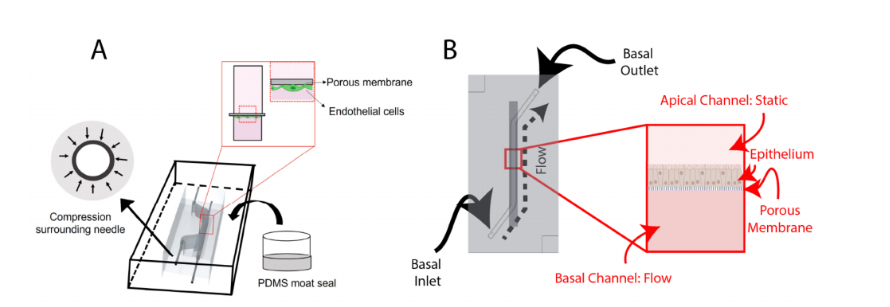
Figure 1.Schematic overviews of: (A) the BBB-on-chip; and (B) the airway-on-chip. Key featuresof the BBB-on-chip include making molds of higher gauge (smaller outer diameter) needles beforeadding the I/O needles and sealing the chip using a PDMS moat. Both chips incorporate a porousmembrane to separate the channels, with the BBB-on-chip seeding endothelial cells basally andthe airway-on-chip seeding epithelial cells apically. Portions of this figure were created usinghttps://biorender.com (accessed on 20 August 2022)
.
Design of the Airway-On-Chip
The airway-on-chip (Figure 1B) channel measures 1.3 mm wide, 0.75 mm high, and25 mm long; these dimensions were chosen to achieve overall culture areas equivalent tocommonly used 24-well Transwell®inserts while maintaining a hydraulic diameter under1 mm to better replicate small airway physiology [36,37].
The airway-on-chip is composed of a monolayer of airway epithelia; as such, itdoes not benefit from the ability for dual-side imaging (or, flipping the chip under amicroscope) enabled by side-loaded fluidics. As such, it employed top-loaded fluidicports, which are partially defined by raised columnar features in the top-layer master moldand hollowing is completed using a tissue biopsy punch (TedPella, 0.5 mm). Importantly,both the diameter of these features in the master mold as well as the diameter of thebiopsy punch is undersized, relative to the 22G needle which is pressure-fit into the PDMS.Additional considerations regarding fluidic port design and integration are provided in theSupplementary Materials.
The mold edge heights define the thickness of the PDMS, which is 6 mm; this value,while large relative to other microfluidic organs-on-chip, was found to impart greater stabil-ity to the stainless-steel needles used to interface fluidics. Alignment features, consisting ofrecessed and protruding squares on the top and bottom chip halves with a 100µm margin,are also included at two corners to assist with manual alignment during fabrication.
2.2. Fabrication and Assembly of the Microfluidic Chips
2.2.1. PDMS Preparation and Bonding
A 10:1 mixture of PDMS elastomer base and curing agent (Dow Sylgard ®184 Silicon Elastomer) was mixed in a planetary centrifugal mixer (Thinky, cat. No. ARE 310) for 90 sat 2000 RPM followed by 60 s at 2200 RPM. The PDMS mixture was casted into the molds and placed into a vacuum chamber for removal of air bubbles in the PDMS mixture for 30–60 min. Following degassing, a transparency film (Apollo, purchased from Amazon.ca (accessed on 9 December 2021)), cut to fit the mold’s footprint with an excess 1–2 cm border, was placed over top of the mold. In order to minimize the formation of bubbles (or air-pockets) forming at the transparency-PDMS surface, a tweezer was used to enable gradual laying of the film from one side to the other of the mold (Figure 2A–D). After placing the transparency, a flat piece of 3/32” thick acrylic was placed on top of the film to enable even compression by an aluminum weight (total weight 200–300 g). The molds Micromachines 2022,13, 1573 5 of 20 were transferred to an oven (65◦C) to cure for at least four hours. Then, the PDMS layerswere removed from the molds using an Exacto-knife, scalpel, or razor blade and excess debris were removed from the surfaces using Scotch™ Magic tape and compressed air.
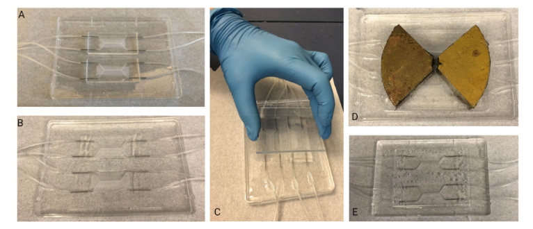
Figure 2.Slowly and carefully placing the transparency film over the uncured, PDMS-filled moldminimizes formation of bubbles: (A–D) depict the different stages of slowly lowering the transparencyonto the convex PDMS surface, starting from the top left corner. A red dotted outline is used to depictthe area of the transparency film that is in contact with the PDMS.
To identify the bonding performance of the PDMS-PDMS or PDMS-glass bonds, first, avisual inspection was made, to ensure all areas of the chip were transparent, then a leak-testwas performed by manually pushing food-colored dyed PBS through tubing attached tothe chip.
Oxygen Plasma Bonding—BBB Chip
For the BBB organ-on-chip application, using tweezers, a membrane (it4ip, cat. No.200M12/620N403/47) was carefully set into position to cover the channel. The two layersof PDMS were treated with air plasma (Harrick plasma cleaner) at ~600 mTorr for 1 minbefore manually aligning the channels and compressing the PDMS layers together forapproximately 30 s. The plasma-bonded PDMS layers were then transferred to a 65◦Coven for at least 2 h to complete the bonding procedure.
Partial Curing—Airway-On-Chip
The airway-on-chip leveraged PDMS-to-PDMS bonding through partial curing, ascharacterized by Eddings et al. [22]. This process comprised an initial, partial cure ofPDMS-filled molds for 60 min at 65◦C following which molds were removed from theoven for membrane alignment, punching, and conjoining the two chip halves. The chipswere then covered with Scotch™tape and returned to the oven under compression foran additional three hours to allow polymerization to complete, yielding a bonded andcomplete microfluidic device.
2.2.2. Fluidic Integration and Reinforcement
BBB Chip
In order to augment the fluidic interface in the side-loading BBB chip, a PDMS encase-ment (“moat”) (Figure 3) was prepared. This encasement was created by taping the tubing inposition, then using a flat, smooth bottom dish into which chips were set. To preserve PDMS,the chips were placed side-by-side and tape was used to keep them together. Then, liquidPDMS was poured around the chips, such that the PDMS surrounded the inlet and outlettubing and fully encased the system. Additionally, a weight was placed on top of the chips tokeep them on the bottom of the dish. Finally, the moat was cured at 65 ◦C overnight.
Figure 3.PDMS Moat Fabrication Steps: (A) Assembled chips are placed into a flat, smooth bottomdish. (B) PDMS is poured into the dish ensuring that the chips are completely surrounded. (C) Anacrylic sheet is placed on top of the chips to ensure the area of interest of the chip (central channel)remains clear of PDMS. (D) A weight is used to weigh the chips down within the liquid PDMS.(E) Once cured, PDMS block is removed from dish. The chips are now embedded in PDMS block andable to be immediately connected to fluidics system
Airway-On-Chip
To improve the robustness of fluidic interfaces and operation of the airway-on-chipover long (≥10 day) culture durations, two approaches were explored and ultimatelyincluded. These consist of: (1) mechanical reinforcement of the reversible PDMS-to-PET-membrane bond through a rigid plastic clamp and (2) fluidic seal enhancement via dispens-ing of uncured PDMS around fluidic interfaces.
The airway-on-chip model features cells cultured on a PET membrane that is sand-wiched between two PDMS microfluidic channels. If the PDMS is not bonded well and thereis a gap between the PDMS and the membrane, cells can grow into the thin gap. This canlead to unpredictable culture sizes and cell numbers, which may undermine reproducibilityfrom chip to chip. Mechanical reinforcement of the reversible PDMS-to-PET-membranebond to restrict cell-growth to the microfluidic channel was found to be necessary andachieved through an acrylic clamp. Quarter-inch cast acrylic (McMaster-Carr, Elmhurst, IL,USA) was purchased in 12”-by-12” sheets and cut with a VLS 2.30 (Universal Laser Systems,Scottsdale, AZ, USA) CO2laser cutter; outer dimensions of the clamp measured 73 mm-by-48 mm, 20 mm larger than the chip along both the length and width. A square cutout(4 mm-by-4 mm) was centered over each fluidic inlet/outlet port to enable access, and twocircular cut-outs sized for 8–32 threaded rods (McMaster-Carr) were made collinear withthe top channel. Compression was achieved utilizing 8–32 thumb nuts (McMaster-Carr)coupled with washers for improved uniformity of force distribution. Following assembly ofthe chip-clamp unit, 22-gauge stainless steel needles (McMaster-Carr) with a 1” 90-degreebend were inserted into the fluidic access ports with the other end of the needle coupled toa 10 cm length of 0.02” ID microbore Tygon tubing (VWR). The other end of this tubinglength was coupled to a 0.5” 22GA straight dispensing tip with a luer-lock connection forease of fluidic interfacing and handling. A strip of tape was placed on the clamp, overtopof the fluidic lines for added stability during handling. Liquid PDMS was, then, dispensedvia pipette (with the tip scissor-cut to increase the opening size, due to the fluid’s viscosity)into the clamp’s cut-outs to augment the compression fit seal between the needles and thePDMS, and cured at room temperature for 48 h. The thickness of the clamp as well as thePDMS of the top chip layer is sized such that the bent stainless steel needle rests on theacrylic when the bent portion penetrates approximately 3.5 mm into the 5.25 mm thick (with the channel depth subtracted from the overall layer thickness) PDMS (not too deep soas to risk piercing the PDMS of the bottom layer while retaining a stable pressure-fit seal).
2.3. Microfluidic Cell Culture
2.3.1. BBB Chip
For the BBB chip, human brain microvascular endothelial cells (HBMECs) (Lonza,Basel, Switzerland, lot# 376.01.03.01.2F) were thawed from passage 6 and used betweenpassage 6–9. HBMECs were cultured onto fibronectin-coated plates and passaged at 80%confluency. Cells were lifted using 0.05% trypsin and cultured with EGM-2 bullet kitcontaining 2% v/v FBS (Lonza, cat. no. CC-3162).
A 1 mL syringe with a 22G dispensing tip was inserted into chip tubing to performall liquid exchanges. For the BBB chip, a 10 min 70% ethanol rinse, followed by two PBSwashes, and an overnight equilibration using EGM-2 media was used to prepare the chipsfor ECM-coating. For the airway-on-chip, a 20 min ethanol incubation preceded coating.
For the BBB chip, a coating of 0.4 mg/mL collagen IV (Sigma Aldrich, St. Louis,MO, USA, cat. no. c5533), 0.1 mg/mL fibronectin (Sigma Aldrich, cat. no. F1141), and0.1 mg/mL laminin (Sigma Aldrich, cat. no. L2020) was applied the day after equilibrationand left overnight in the fridge. Lastly, the chip was washed twice with PBS. Then, HBMECswere seeded into the chip at a density of 5 million cells/mL and then attached to a pumpfor at least 5 days to allow for perfusion through the endothelial channel. A syringe pumpwas used to provide media perfusion resulting in shear stress values of ~0.001 dyne/cm2within the channel. The top channel media was exchanged every two days. The profile ofthe flow rate delivered by the syringe pump was measured using microfluidic flow sensors,as described in the Supplementary Materials.
2.3.2. Airway-On-Chip
Three vials of Calu-3 human lung adenocarcinoma airway epithelial cell line wereobtained from ATCC and expanded and maintained in T-75 flasks using Eagle’s MinimumEssential Medium (Corning, Corning, NY, USA) supplemented with fetal bovine serum(MilliporeSigma, St. Louis, MO, USA, Cat: F1051, Lot: 19D019), and Antibiotic-Antimycotic(Thermo, Waltham, MA, USA, Cat: 15240-062, Lot: 2441423). Cells were passaged at 80%confluence and used for experiments between Passages 20–25.
Microfluidic chips were filled with a 100µg/mL rat-tail-collagen (Corning, Cat: 354236,Lot: 1049001) solution in PBS and incubated in a biosafety cabinet overnight to completemembrane coating. Following flushing and equilibration with complete culture medium,chips were seeded via syringe-infusion with a suspension containing six-million cells permilliliter. After the suspension was loaded, luer caps (McMaster-Carr) were coupled toeach fluidic line and the chips were transferred to an incubator to allow cells to attach forfive hours.
Following the five-hour attachment period, luer caps were removed from the basalchannel inlet and outlet lines. They were, then, connected to a recirculating flow sys-tem, wherein a peristaltic pump was positioned to pull culture medium through thebasal channel and into a 2 mL medium reservoir containing the same medium used forculture maintenance. The recirculating flow regime enables the application of physiolog-ically relevant shear stresses while minimizing reagent consumption. Reservoir culturemedium was contained in five milliliter screw-cap MacroTubes™(FroggaBio, Toronto, ON,Canada); their caps were punctured with 16-gauge needles (Becton, Dickinson and Com-pany, Franklin Lakes, NJ, USA), creating an opening just large enough to accommodatethe insertion of the microfluidic tubing employed. The tubing expands in the warmerenvironment of the CO2cell culture incubator, creating a tighter seal for the duration ofthe experiment. The following day, the apical channel was washed with fresh completemedium, and maintained in a submerged state for the duration of the experiment.
The reservoir volume was chosen based on manufacturer’s recommendations forTranswell®24-well culture inserts; this recommendation stipulates a culture volume of 600µL to support a culture area of 0.33 square centimeters, equivalent to the airway-on-chip. Exchange of medium in a Transwell plate every two days is a common culture regimethat has been demonstrated to produce functional cultures [38,39]. Direct communicationwith ATCC yielded an upper bound on culture medium stability in a cell-culture incubatorof four days, and this exchange interval has been employed in previously reported organ-on-chip cultures; as such, the 600µL value was doubled to 1.2 mL and a factor of safetywas added to arrive at the 2 mL reservoir volume, with reservoir exchanges and apicalchannel washes taking place every three to four days [40]. The initial flow rate employedwas 300µL/min, which was ramped up following the second media reservoir exchangeand apical channel wash to 540µL/min, corresponding to a wall shear stress between 0.6and 0.7 dyne per square centimeter exerted basally at the higher flow rate—small airwayepithelia experience a range of 0.5–3 dynes per square centimeter at rest due to airflowin vivo [10,41].
Cultures were maintained for eleven days, at which point Calu-3 epithelia cultured onTranswell inserts reach peak barrier integrity (measured based on apparent permeability tofluorescein isothiocyanate-conjugated dextrans) [39].
2.4. Cell Culture Analysis
2.4.1. BBB Chip
HBMECs were stained to visualize f-actin and nuclei. All staining was performed in-chip. A 1 mL syringe with a 22G dispensing tip was inserted into the chip tubing to performall liquid exchanges. For f-actin staining, samples were fixed, with 4% paraformaldehydein PBS and left at room temperature for 15 min. Samples were washed twice with PBS for10 min. After washing the fixative 2×5 min with PBS, samples were incubated with the66µM dimethyl sulfoxide (DMSO) Alexa-Fluor-488 Phalloidin stock solution at a 1:400dilution in PBS for 1 h at room temperature. Samples were left in a dark, covered containerto prevent photobleaching and evaporation while staining. Then, samples are washed2×5 min with PBS (1×). For nuclei staining, cells were either stained live or fixed,with Hoechst (Thermofisher Scientific, Waltham, MA, USA, cat. no. H3570) at a 1:1000dilution in EGM-2 or PBS. Live cells were washed with EGM-2 and fixed cells were washed2×5 min with PBS (1×).
BBB chips were disassembled using an Exacto knife and pliers, and the membranewas removed and placed onto a glass slide with tweezers. The membrane was placedwith the cell side facing upwards. ProLong®gold Anti-Fade containing 40,6-diamidino-2-phenylindole (DAPI) was used to mount the membrane and a cover slip was placed ontothe membrane; because the cells were stained with Hoechst, the DAPI was not necessarybut was included in the commercial formulation. The edges of the coverslip were sealedusing clear nail polish to prevent evaporation. The mounted samples were stored at 4 ◦C.
2.4.2. Airway-On-Chip
On Day 11, the airways-on-chip were fixed in situ for preservation and staining. Allsteps involving manual syringe-infusion of chips are conducted separately for each channel,while the other is occluded; for example, when washing with PBS, the apical channel iswashed first while the basal channel is closed with luer-caps. Infusion of a channel isconfirmed both visually in the channel, for example by tracking small bubbles that may beintroduced during injection, as well as via confirmation of three droplets forming at theoutlet of the channel being infused (chosen conservatively, based on the internal volumeof the channel). The single-channel infusion with the second channel blocked minimizedthe chance of crossflow, which is especially important earlier in the experiment when cellshave not adhered or formed a barrier tighter than the porous membrane itself.
Chips were washed with PBS three times; following this, a 4% methanol-free formalde-hyde solution in PBS (Thermofisher, Pierce) was infused to fill each channel. This solutionwas incubated for 15 min at room temperature, following which an additional three PBSwashes were performed. Cells were then permeabilized by injection of a 0.02% Tween-20 solution in PBS, which was incubated for 15 min followed by an additional three PBSwashes. Chips were then blocked with a 1% BSA solution for 90 min before loading theworking concentration of Alexa-Fluor 488 Phalloidin (Thermofisher) stain (165 nM in PBScontaining 1% BSA), which was incubated for 45 min. Chips were, then, washed a finalthree times before fluidic and clamp disassembly.
Four incisions along each edge of the membrane, through the PDMS, were madeto extract the cell-laden membrane from the chip. Extracted membranes were promptlylaid onto a microscope slide with two drops of ProLong Gold antifade reagent with DAPI(Thermofisher); a coverslip was carefully placed atop the membrane and the mountingmedia was cured under a coverslip at room temperature in the dark overnight. Thefollowing morning, slides were transferred to a slide-box for storage at 4 ◦C.
2.5. Imaging
Images of HBMECs were taken on an inverted microscope (Zeiss, Observer.Z1,Oberkochen, Germany). Images of Calu-3s were taken on an inverted microscope withepifluorescent capabilities and intermediate magnification switching from 1.0×to 1.5×(Nikon Eclipse Ti2-E (Nikon, Tokyo, Japan)); 10×/NA 0.3, dry (Nikon: MRH10105) and40×/NA 0.6, dry (Nikon: MRH48430) objectives were used in conjunction with 432 nm(Semrock, Rochester, NY, USA, 36 nm bandwidth, cat: FF01-432/36) and 515 nm (Sem-rock, 30 nm bandwidth, cat: FF01-515/30) single bandpass emission filters for DAPI andAlexa-Fluor-488-Phalloidin microscopy, respectively).
2.6. PDMS Thickness Uniformity Characterisation
In microfluidic devices employing pressure clamps to aid in sealing (such as thatdepicted in Figure 4), the thickness uniformity of the PDMS critically impacts both thequality of the seal as well as channel integrity. Thickness nonuniformity can lead to unevencompression across the device, in turn leading to leakage in regions of low compressionor channel deformation in regions of higher compression. We introduced the use of trans-parency films during curing to improve thickness uniformity and thus device performance.In order to characterize the impact of employing transparency films during PDMS curing, aseparate PDMS microfluidic device with two, smaller, microfluidic channels was fabricatedthat would better highlight channel integrity under compression. Master molds werecreated on the same printers as for the organ-on-chip devices and fabrication methodswere identical to the organs-on-chips. Three devices were fabricated without the use of atransparency film to quantify its effects on the flatness of a cured device, and three deviceswere fabricated with a transparency film for comparison.
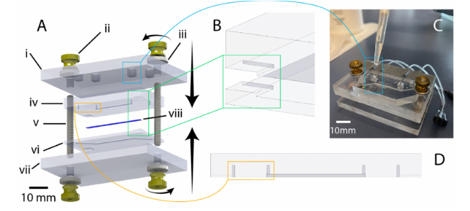
Figure 4.Illustration of chip design and highlighting of critical features. (A) exploded view of chipcomponents (created using SolidWorks): i: 1/4-inch-thick acrylic top clamp, ii: 8–32 brass flanged thumb nut, iii: 8–32 oversized washer, iv: PDMS chip (top half), v: 8–32 threaded rod (1.5” length), vi: PDMSchip (bottom half), vii: 1/4-inch thick acrylic bottom clamp, viii: PET membrane. (B) illustration ofcorner alignment features to assist manual mating of chip halves during bonding. (C) Illustrationof liquid-PDMS reinforcement of fluidic port seal via pipetting of uncured PDMS into top-clampcutouts. (D) Highlighting of punch guides to assist in the accurate positioning and clear formation ofmanually punched through-holes for fluidic connection.
Following fabrication, the PDMS devices were measured with calipers at the same fivepoints equally spaced along the long edge of the device. The devices were then compressedagainst a silicon wafer and visualized under a brightfield epi-illumination microscope(Aven MicroVue (Aven, Ann Arbor, MI, USA)) to assess the deformation of channels.Compression was achieved using 3–32 bolts and a rigid, laser-cut, cast-acrylic washer;the same individual manually screwed the bolts using fingertips to achieve comparablecompression across all tested devices.
2.7. PDMS and Mold Surface Roughness Characterisation
The surface topography and surface roughness of the mold interior and the subsequentPDMS gasket was investigated with an atomic force microscope (AFM). The images ofthree random spots on each respective surface were obtained using a Nanosurf EasyScan 2AFM system (Nanosurf, Liestal, Switzerland) in tapping mode with Si tips over the threeregions of area 10µm×10µm with a 512×512 pixel resolution. The root mean square(RMS) was then calculated to quantify surface roughness.
3. Results
3.1. Surface Roughness of 3D Printed Molds
A visual comparison between the PDMS casted in both SLA and DLP molds is shownin Figure 5A,B, while surface roughness characterization is presented in Figure 5C,D. Themanufacturer’s stated x-y as well as z resolutions of the DLP printer (MiiCraft Ultra 50) are30µm and 5–500µm, respectively; corresponding values for the SLA printer (FormlabsForm2)—x-y and z resolution—are 140µm and 25–100µm. The z-resolution is user-selectable, and the values employed during mold fabrication were, for the DLP and SLA,30 and 25µm, respectively. The DLP printer used in this work was made specifically forPDMS casting, as the PDMS master mold resin is made with methacrylated monomers andoligomers and the light engine is optimized for this resin, allowing for an improved surfacefinish and minimal contact inhibition of PDMS curing (common in other 3D printing resinsdue to photoinitiators present in those resins) [42]. The resin in a DLP printer is curedlayer-by-layer using a light projector and not point-by-point using a laser beam as in a SLAprinter. We hypothesized that the difference in resolution between the two printers, as wellas the layer-by-layer curing process, may be expected to contribute to reduced roughnessin the printed molds. Figure 5A,B, illustrated that a PDMS microfluidic device casted onthe DLP printer exhibits improved optical clarity compared to the PDMS microdevice thatwas casted using an SLA mold, likely due to the decreased scattering resulting from lowersurface roughness of the DLP-printed mold. Measured surface roughness, correspondingly,was generally lower on the DLP-printed mold. Average RMS (root mean squared) surfaceroughness (±standard deviation over three areas measured) achieved using the DLP printerfor the mold and casted PDMS were 64.7±15.8 and 65.3±6.7 nm, respectively. Whenusing the SLA printer, mold and casted PDMS RMS surface roughness were288.9 ±298.9and 209.63±91.5 nm, respectively. A one-sided Mann–Whitney U test was performed tocompare RMS roughness across both the DLP and SLA molds as well as the PDMS casttherein; the p-value associated with the comparison of molds was 0.2, while for the castPDMS p= 0.05. Although these results did not indicate statistical significance over thepresented measurements, this might be attributable to insufficient sample size (particularly impactful in non-parametric statistical tests), as we qualitatively observed less leakage andimproved optical transparency with PDMS fabricated using the DLP printer.
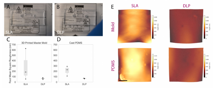
Figure 5.Comparing the performance of rapidly prototyped master molds. (A,B) comparison imagescaptured of PDMS devices superimposed upon fine-point text to highlight optical clarity: (A) devicecast from Form2-SLA-printed mold; (B) device cast from MiiCraft-DLP-printed mold. The devicecast from the DLP-printed mold shows improved optical clarity. (C,D) boxplot summarizing RMSsurface roughness of SLA and DLP molds alongside corresponding cast PDMS. Individual datapoints are represented as black dots superimposed on a boxplot, where the box height representsthe interquartile range, the whiskers the total range, and the central line the median value. Whilestatistical significance was not achieved, a trend towards lower roughness associated with DLP-printed molds and corresponding cast PDMS was exhibited—manifesting through the improvedoptical clarity illustrated over Subfigures (A,B). (E) representative topographic images obtainedthrough AFM characterization of DLP and SLA 3D printed master molds (top) and cast PDMS(bottom); color scale corresponds z-axis height (surface profile), illustrating a more uniform surfaceobtained on the DLP-printed mold and cast PDMS. Scale bar represents 2.5 µm.
3.2. PDMS Thickness
Manual pouring of PDMS into master molds will generally result either in a slightoverfilling or underfilling of the mold. The former manifests as a dome-like concave profilewhen viewed from the side; the latter results in the opposite as well as particularly starkheight non-uniformity around features within the mold, especially when feature height iscomparable to the depth of the mold. Furthermore, if the surface upon which the mold isresting during curing is not flat, a slant along the surface of the cured PDMS will developcorresponding to the angle of the curing surface. In order to overcome these effects (relatedto surface tension and/or surface angles), commercially available copier transparency filmwas used to provide a temporary lid (under an aluminum weight) to an overfilled moldthat could be peeled off following curing to reveal a microfluidic device with more uniformthickness. Figure 6highlights the thickness artefacts near features as well as their mitigationusing the transparency film; thickness characterization of three devices fabricated with andwithout transparency films yielded a statistically significant increase in uniformity acrossthe length of microfluidic devices fabricated with a transparency film (depicted graphicallyin Figure 6D).
Concerns surrounding non-uniformities in PDMS microdevice thickness include theincreased likelihood of channel deformation under compression, commonly employedto augment fluidic seals and integrity for organ-on-chip applications (as discussed in theAirway-on-Chip subsection of Section 2.2.2, pertaining to clamp design) [33]. Figure 7illus-trates this phenomenon; channels in microfluidic devices fabricated without a transparency(less uniform in thickness) exhibit greater deformation under comparable compressive load. In quantifying the flatness uniformity, we observe much larger inter- and intra-devicevariability for devices fabricated without transparency than those fabricated with ourtransparency method (quantified interquartile range of 125µm with transparency, and1.225 mm without in Figure 6C; interquartile range of 4 µm with transparency, and 55 µmwithout in Figure 6D.
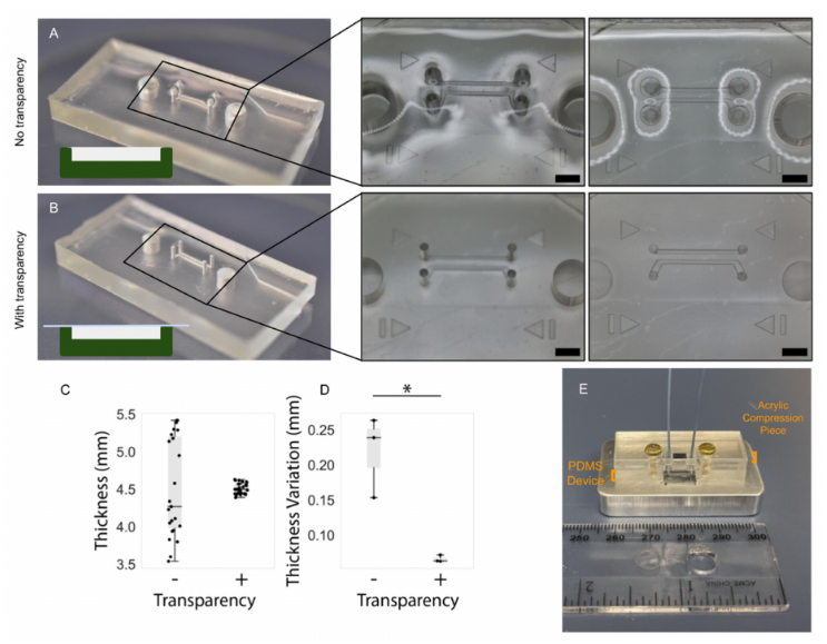
Figure 6.PDMS device fabrication with the transparency film method improves the flatness anduniformity of the top PDMS surface. Comparison of uniformity in PDMS thickness: (A) in absence oftransparency film and; (B) when employing transparency film method, scale bar (black) represents2 mm. Insets depict warping of the surface of the PDMS device fabricated without the transparencymethod, in regions surrounding the through-hole structures in the mold (visible as reflections andoptical aberrations). In contrast, the surface of the device fabricated using transparencies is flat anddoes not impart these optical aberrations. (C) Comparing the impact of the transparency film onthe measured thickness at several points on replicate PDMS devices and; (D) on the intra-devicevariability in PDMS thickness measurements taken at different regions on PDMS devices. The 15 rawthickness measurements for each set of devices is plotted in (C) and the standard deviation of thefive measurements corresponding to each device is plotted in (D) (the asterisk denotes statisticalsignificance at the 5% level). Individual data points are represented as black dots superimposed on aboxplot, where the box height represents the interquartile range, the whiskers the total range, and thecentral line the median value. (E) Illustration describing application of PDMS: microchannels moldedinto PDMS are sealed against a silicon wafer device to be subjected to flow via compression of a rigid,laser-cut, acrylic piece where non-uniformities in PDMS thickness may undermine the PDMS sealand flow path integrity.
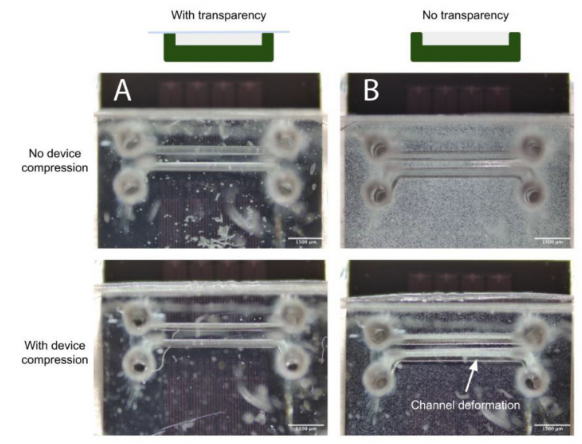
Figure 7.(A) When employing the transparency film during casting, the improved PDMS thicknessuniformity facilitates straightforward reversible PDMS bonding using a compression setup; (B) Uponcompression of the device against a flat surface to enclose the channels, increased channel deformationis evident under comparable force when employing a device fabricated without a transparency film.
3.3. PDMS Encasement for Leakage Prevention: Comparison with Traditional Epoxy
We have determined that a combination of a compression-fit port, made using a highergauge needle in the PDMS molding process, with a surrounding PDMS fortification or moatserves as a simple and effective method for connecting tubing to PDMS chips. Utilizing aPDMS moat-based method to reinforce fluidic connections rather than clamping or epoxyprovides more flexibility within the device design. When combined with side-loaded ports,a PDMS sealing method can increase the devices compatibility with needle based sacrificialmolding techniques used for creating 3D lumens with circular geometries.
A common method to reinforce and secure ports/fluidic connections on PDMS mi-crodevices includes utilizing epoxy to fix and seal tubing and/or needles in place [43]. Theepoxy is used to seal any opening to prevent leakage and to prevent fluidic ports fromdisconnecting from the system during perfusion. However, for long term cell culture, epoxycan degrade over time resulting in delamination and separation between the epoxy-PDMSinterface, as seen in Figure 8. An accelerated version of this separation was demonstratedby submerging chips sealed with epoxy or PDMS moats in 70% ethanol for 24 h. After24 h, devices reinforced with epoxy showed signs of delamination and degradation whilethose reinforced with a PDMS moat did not. This indicates that for longer term cell cultureutilizing a PDMS moat style of reinforcement may be more suitable for leakage prevention.
3.4. Success Rate of BBB Chips
BBB chips were seeded with endothelial cells and perfused with media for five days,and their performance was evaluated at different checkpoints. To assess the microfluidicchip performance, an initial checkpoint (Checkpoint 1) was used to identify if the PDMS-PDMS bonding was sufficient. To evaluate this checkpoint, a visual inspection was madeafter the bonding of the PDMS layers to ensure they were transparent, and also a manualleak test was performed. A second checkpoint (Checkpoint 2) was used to identify ifany chips had leaked after being perfused with media for five days. This checkpoint was evaluated by visual inspection to ensure no tubing had disconnected or any leaks occurreddue to insufficient bonding of PDMS or disconnected fluidic interconnects. Betweencheckpoints 1–2, there were 88% of 17 chips that had been viable after five days on pump.In this case, the failure mode was due to a tubing line becoming disconnected from thedispensing needle that contained a syringe full of media.
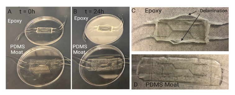
Figure 8.Investigating PDMS device sealing method. Sealing with PDMS moat prevents delaminationduring cell culture period. Comparison of degradation of sealing methods over 24 h: (A) Samplesare submerged in 70% ethanol to accelerate the degradation seen in other aqueous liquids such ascell culture media. When initially placed in ethanol there are no visual signs of degradation in chipssealed with epoxy and chips sealed with a PDMS moat. (B) After 24 h, the ethanol in which the chipseal with epoxy is submerged exhibits a discoloration indicating a degradation of the epoxy. The chipsealed with PDMS moat shows no signs of discoloration or breakdown. Visual inspection of chipssealed with (C) epoxy and (D) PDMS moat (D) after 24hrs of submersion in ethanol. Over 24 h ofsubmersion, the Epoxy-PDMS interface begins to delaminate and separation between the two layerscan be seen macroscopically. This separation results in limited support for preventing leakage inchips when higher pressures are experienced within the device.
As some chips had endothelial cells seeded on Day 0 of the experiment, an additionalcheckpoint (Checkpoint 3) was used to identify if any cells attached to the membrane.This checkpoint can have many common failure modes, as it coincides with the cell layeroptimization process. These failure modes could include cell detachment due to an unevenextracellular matrix layer, an air bubble trapped in the channel, or even insufficient mediasupply. Lastly, a final checkpoint (Checkpoint 4) was used to assess if there was a confluentmonolayer of endothelial cells present. This was assessed with a visual inspection, and itshould be noted that future optimization could be needed to ensure the monolayers presentcan be used in functional assays, such as a permeability assay. In this case, since onlyapproximately half of the chips were seeded with cells (and the other half acted as controls),out of the eight chips seeded with endothelial cells, 57% formed a confluent monolayer,based on visual assessment. Table 2outlines the checkpoints and their respective commonand suspected failure modes.
3.5. Cell Proliferation and Morphology
The BBB chip was seeded with HBMECs and perfused with media using a syringepump for five days. As demonstrated in Figure 9, the cells adhered and remained on themembrane throughout the culture period. Based on visual assessment, the three chipsshown produced a confluent HBMEC monolayer. The fabrication methods used with thisBBB chip demonstrate the potential for a confluent monolayer to be formed and furtheroptimized to be able to be used in functional assays. A common functional assay that issuitable for use with this chip is a permeability assay, which often relies on fluorescently labeled dextran being perfused through the channel of the chip, and sampled at differenttime points within the same (bottom) channel and the top channel [44,45]. A functionalassay allows the user to assess the quality of the microtissue by obtaining a baselinemeasurement before adding any therapeutic or damaging treatments.
Table 2.An overview of the checkpoints used to assess the outcome of different stages in the BBBchips timeline. These checkpoints include PDMS bonding, media perfusion, cell attachment and theformation of a confluent monolayer. Common and suspected failure modes are also described.
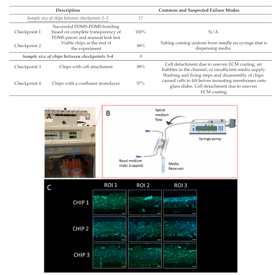
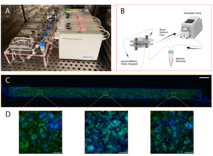
Figure 9.Illustration of blood–brain barrier chip cell culturing protocol and representative results:(A) Configuration with five chips in a cell culture incubator with medium reservoirs and pumping set-up; (B) Schematic illustrating culture environment of single chip, with apical channel static and syringe pump flow through basal channel of the BBB chip, created with BioRender.com; (C) Stitched mi-croscopy image comprised of images capturing three regions of interest (ROIs) of the membrane postextraction and immunofluorescence staining (scale bar: 200 um), the green stain is phalloidin, andthe blue stain is Hoechst 33342.
For the airway-on-chip, 71% of the 14 chips cultured with the methods described inSections 2.1–2.3 produced extracted membranes with a confluent layer of airway-epithelia(depicted in Figure 10). Of these, all displayed the characteristic cobblestone-like mor-phology under F-actin immunofluorescence staining and were confined to the channel(as evidenced by the strict rectangular shape of the stained cells in Figure 9C). Consistentproduction of morphologically typical airway epithelial allows suchin vitromodels to beemployed in applications such as aerosol inhalation studies, where the apical chambermedium can be replaced with air or aerosols of interest (for example cigarette smoke ordiesel exhaust) [46,47].