Electronic Supplementary Information (ESI): 3D Printing-Enabled Uniform Temperature Distributions in Microfluidic Devices
Derek Sanchez , Garrett Hawkins, Hunter S. Hinnen, Alison Day, Adam T. Woolley, Gregory P. Nordin, Troy Munro
Several steps were followed when optimizing basic designs for isothermal temperature distributions. They were to model a basic design, evaluate the design, modify the design, and repeat.
We kindly thank the researchers at UCLA for this collaboration, and for sharing the results obtained with their system.

Methods for Optimizing Temperature Distributions
1.1 Model a Basic Design
The first step, to model a basic design, requires that you have a basic heater design in mind. The chip is modeled using a CAD software package, such as OpenSCAD or SOLIDWORKS. The use of parametric modeling techniques will make any modifications that need to be made much easier to implement. The chip (with voids for the channels), the heater, and any other filled channels will have to have separate CAD models. The CAD design is then imported into a finite element analysis (FEA) software package, such as COMSOL Multiphysics. See the methods section for suggestions of which boundary conditions to use.
1.2 Evaluate the Design
The second step, evaluating the design, utilizes the COMSOL simulation mentioned in the previous step. The simulation is evaluated using cut planes (or the equivalent for software packages other than COMSOL) placed as depicted in figure 1. The planes are then analyzed using surface and contour plots, such as in figure 2.
The surface plot helps to see large changes over the plane. Typically, we reduce the color and data ranges so that only the area directly around the volume of interest is shown. The contour plot helps to see small changes and how the temperature “flows”. Typically, we will set the range of the data to the same range as the surface plot and will use different level spacing depending on what is seen on the surface plot. Another plot that is used to evaluate the designs is a line graph of a cut line through the center of the volume of interest in the X direction. Such a plot can be seen as the ABC line in figures 4 and 6 of the main publication.
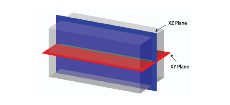
Fig. 1 Depiction of cut planes made for the purpose of analyzing a design
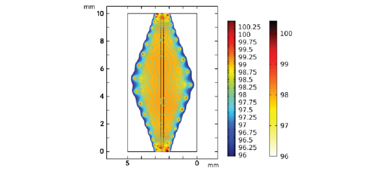
Fig. 2 Surface and contour plot for the xy Plane of the Tapered Helix Design. 0.05 mm tiers are used for the contour plot.
1.3 Modify the Design
Once the previously mentioned plots are made, they can be analyzed to see what changed need to be made. The process we typically follow is to use the line plot of line ABC to identify areas where there are large changes in temperature. Depending on if these temperatures are higher or lower than their surrounding temperatures, the heating channel can be brought further or closer to the volume of interest.
As an example, figure 4 of the main publication shows the line plot for the helical design. It can be noticed that the temperature decays significantly as it nears the ends of the volume of interest and is the hottest at the center. Based on these findings, The diameter and pitch at the ends of the helix were reduced so as to provide more heat to the volume of interest. The diameter and pitch at the center of the helix were increased so as to provide less heat to the volume of interest.
The surface and contour plots can be used in a similar way. In the example of figure 2, an xy cut plane of the tapered helix design is shown with .05 degree levels. It can be noticed that the negative x side of the channel is slightly warmer than the positive x side of the channel. It can also be noticed that the middle of the channel is slightly cooler than the millimeter on either side of it. If we were going to try and improve this design even further, we would attempt to make the diameter at the center of the chip slightly smaller and perhaps slightly increase the diameter of the helix at x = 0 to help reduce the uneven heating.
One suggestion for this step is to only change one thing each time through the cycle. This will help isolate whether a change is helping or hurting the temperature distribution. If multiple parameters are changed and the temperature distribution is not as one would expect, it can be much more difficult to identify which change caused the decrease in performance.
1.4 Repeat
The changes suggested in the last step would then be made in the CAD model and the simulation would be run and analyzed again. This process is followed until an acceptable design is created. Figure 3 shows the results of this process for the improvement of the serpentine heater to the non-planar serpentine heater. Figure 4 show the results of this process for the improvement of the box heater to the diamond heater.
2 Physical Chip Creation
2.1 3D Printing
As mentioned in the introduction of the main publication, 3D printing microfluidic devices overcomes limitations and complexities of other fabrication methods. Figure 5 presents a graphic of simplified device creation. Main advantages are the lack of using molds, aligning layers, and bonding layers. Those processes can often necessitate a clean room environment.
As mentioned in the introduction of the main publication, 3D printing of microfluidics can be separated into two groups, indirect printing and direct printing. In indirect printing, 3D printers are used to create casting molds for devices typically made of polydimethylsiloxane (PDMS) 1 . Direct 3D printing creates the device that will be used, not the mold. There has been significant work in 3D printing of lab-on-chip devices via stereolithography (SLA), PolyJet (PJ), or fused deposition modeling (FDM). Extensive work has been done in this field to improve direct 3D printing of microfluidic devices 2–4, but many devices are still printing in the millifluidic regime with internal features larger than the resolutions manufacturers advertise 5 .
There is an important difference in 3D printed microfluidics between having spatial resolution of projected pixels (for SLA) of several µms and motor position (which can do well for printing some surface features) compared to producing voids within the interior of the microfluidic device. In other words, layer and pixel resolution is not the same as feature resolution. To overcome this issue of 3D printing being limited to millifluidic devices, twophoton Direct Laser Writing (DLW) Polymerization is often cited6 as the solution because of its submicron resolution, but DLW is severely limited to small build dimensions and long build times as each voxel needs to be built sequentially 7 . This limitation means DLW has rarely 8–10 constructed an entire device, and is instead used to create high resolution components in an already created device 11 .
As mentioned in the introduction of the main publication, our previous work has developed an SLA printer that is capable of voxel sizes of 7.6 × 7.6 × 10 µm 12, producing internal features as small as 18 × 20 µm 13. This is a drastic improvement on all commercial 3D printers (excluding DLW printers), including the recently released CADworks3D PROFLUIDICS 285D, with internal feature sizes of 80 µm and 28.5 µm XY resolution14 .
2.2 Liquid Metal Filling
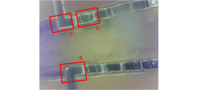
As mentioned in the validation section of the main publication, the temperature profile of a microfluidic device filled with liquid metal may differ from a model’s prediction if there are sharp corners in the device. In Figure 6 we show a photo of an un-filled and filled corner in a 3D printed chip.
Notes and references
1 W. Jung, S. Lee and Y. Hwang, Smart Materials and Structures, 2022, 31, 035016.
2 K. Ogishi, T. Osaki, Y. Morimoto and S. Takeuchi, Lab on a Chip, 2022, 22, 890–898.
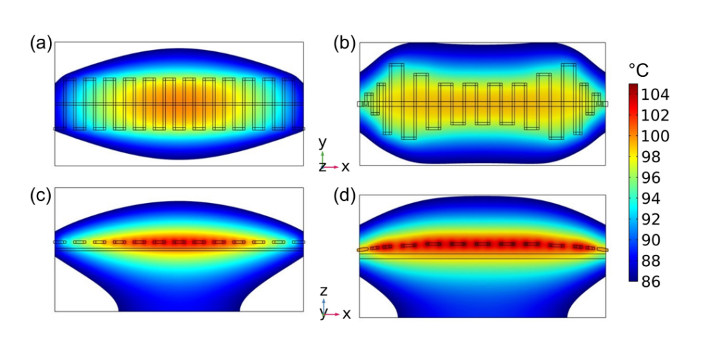
Fig. 3 Temperature map plots of (a,c) the serpentine and (b,d) the non-planar serpentine. The internal temperature distributions are presented with (a,b) a top view (xy-plane) cut through the middle of the chip and target volume and (c,d) a side view (xz-plane) cutting through the middle of the chip and target volume. The color scales are the same in all views to visually compare the degree of spatial temperature stability improvement. Some areas are blank due to the color scale being focused on the higher temperatures to increase temperature gradient visibility. The target volume in the spiral heater chips goes through many colors showing a low level of spatial temperature uniformity. The target volume in the tapered helix has fewer color changes, showing improved spatial temperature uniformity.
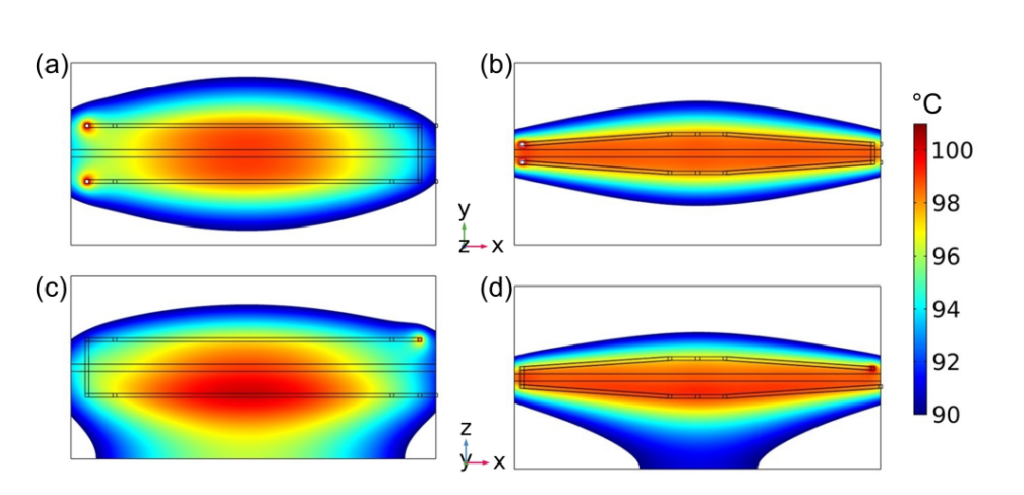
Fig. 4 Temperature map plots of (a,c) the box and (b,d) the diamond. The internal temperature distributions are presented with (a,b) a top view (xy-plane) cut through the middle of the chip and target volume and (c,d) a side view (xz-plane) cutting through the middle of the chip and target volume. The color scales are the same in all views to visually compare the degree of spatial temperature stability improvement. Some areas are blank due to the color scale being focused on the higher temperatures to increase temperature gradient visibility. The target volume in the spiral heater chips goes through many colors showing a low level of spatial temperature uniformity. The target volume in the tapered helix has fewer color changes, showing improved spatial temperature uniformity.
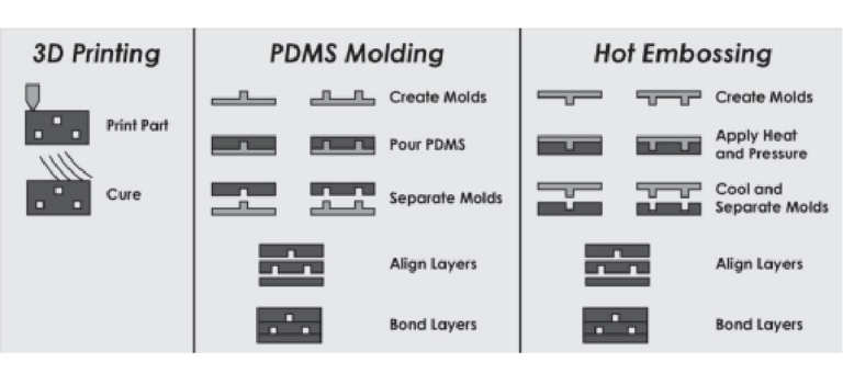
Fig. 5 Common fabrication methods for microfluidic devices.