
Research Article Summary
5 Minute Read
UTS Researchers 3D Print Inertial Microfluidic Chips Directly From CAD, No Mold or Cleanroom Needed
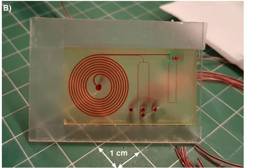
Title
3D-Printing of Inertial Microfluidic Devices
Authors
Sajad Razavi Bazaz, Omid Rouhi, Mohammad Amin Raoufi, et al.
Journal
Scientific Reports, (2020)
DOI Link
Summary
Bazaz et al. developed a direct 3D printing workflow for building inertial microfluidic devices, replacing PDMS molds and cleanroom lithography with a 3D printed channel bonded to a transparent sheet using adhesive tape. The process takes a design from CAD file to a tested, working chip in under two hours, and enabled the team to build a triangular spiral channel that standard lithography cannot produce.

Summary Author
This page was prepared by CADworks3D to summarize and highlight a peer-reviewed research article authored by independent researchers utilizing the CADworks3D system.
Title
3D-Printing of Inertial Microfluidic Devices
Authors
Sajad Razavi Bazaz, Omid Rouhi, Mohammad Amin Raoufi, et al.
Journal
Scientific Reports, (2020)
DOI Link
Key Results at a Glance
< 2 Hours
Fabrication Time
From CAD file to a tested, working microfluidic chip
150 psi
Bonding Strength
Withstands nearly 3x the pressure of a typical PDMS chip before leaking
5 Channel Geometries
Design Versatility
Straight, spiral, serpentine, curvilinear, and contraction-expansion channels, all printed directly
< 300nm
Surface Roughness
Smooth enough to leave particle focusing and fluid flow undisturbed
Objective
Inertial microfluidics uses the shape of a microchannel, not pumps, valves, or fluorescent labels, to sort particles and cells. Fluid moving through a channel at the right speed pushes particles into predictable positions across the channel’s cross section, and where those positions land depends entirely on the shape of that cross section. This principle already drives tools for isolating circulating tumor cells, separating blood components, and sorting bacteria, and it functions as a passive, label-free alternative to techniques like fluorescence-activated cell sorting.
That dependence on geometry creates a fabrication bottleneck. Most inertial microfluidic chips are made by casting PDMS over a master mold, and the mold itself is produced using silicon etching, SU8 lithography, or precision micromilling of aluminum or PMMA. These methods work, but they are slow, costly, and limited to shapes a cleanroom or a milling bit can physically cut. Curved, non-rectangular, or sharply cornered cross sections, such as a right-angled triangle, are difficult or impossible to mold this way. Other approaches, including laser ablation and hot embossing, remove one obstacle while introducing another, whether that is a rough channel wall or the need for specialized equipment.
Direct 3D printing looked like an obvious way around these constraints, but earlier attempts ran into a different wall. Resins used in SLA and DLP printers are rarely transparent enough for microscopy, and printed channels needed to stay at the millimeter scale rather than the micrometer scale most inertial applications require, since leftover resin is difficult to clear from very fine features.
That left a real gap: no single fabrication method combined the geometric freedom of 3D printing with the optical clarity, micrometer-scale precision, and fast, low-cost workflow that inertial microfluidics research actually needs. Closing that gap is what this study set out to do.
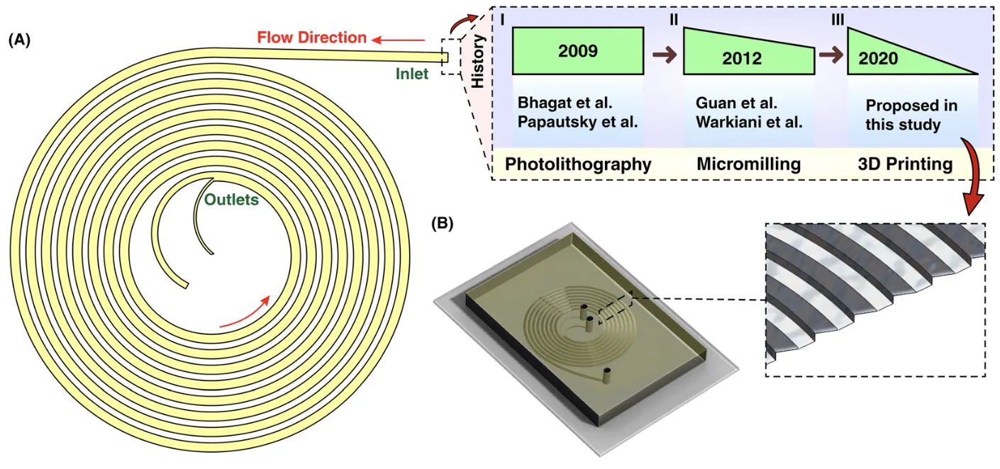
Figure 1. (A)Three generations of spiral channel fabrication: photolithography in 2009, micromilling in 2012, and direct 3D printing in this study. (B) CAD schematic of the right-angled triangular spiral channel, 600 µm wide and 210 µm tall at the inner wall, a cross-section standard lithography cannot produce.Source citation: Source: Bazaz et al. 3D Printing of Inertial Microfluidic Devices. Scientific Reports. 2020.
Methodology and Design
The core of the method is straightforward. A channel is designed in CAD software, printed directly on a high-resolution DLP/SLA 3D printer, cleaned, and bonded to a transparent PMMA sheet with double-sided adhesive tape. No PDMS, no master mold, and no cleanroom step appears anywhere, and a finished, testable chip is ready in well under two hours.
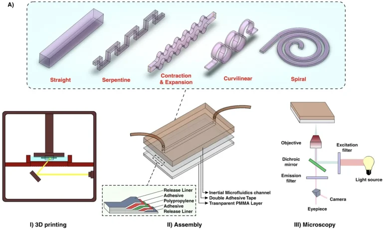
Figure 2. The fabrication workflow: the channel is 3D printed, bonded to a PMMA sheet with adhesive tape, then imaged from the transparent underside using standard microscopy. Source citation: Source: Bazaz et al. 3D Printing of Inertial Microfluidic Devices. Scientific Reports. 2020
To prove the method could handle the geometries that matter most in inertial microfluidics, the team printed and tested four designs:
Straight Channel
Serpentine Channel
Spiral Channel
Triangular Spiral Channel
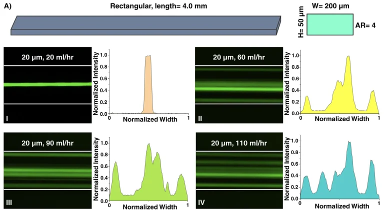
Figure 3. Design of the straight test channel: 200 µm wide, 50 µm tall, with an aspect ratio of 4. Source citation: Source: Bazaz et al. 3D Printing of Inertial Microfluidic Devices. Scientific Reports. 2020.
Figure 4. CAD schematic of the right-angled triangular spiral channel, 600 µm wide and 210 µm tall at the inner wall, a cross-section standard lithography cannot produce. Source citation: Source: Bazaz et al. 3D Printing of Inertial Microfluidic Devices. Scientific Reports. 2020.
The straight rectangular channel, the simplest and most common inertial geometry, focused 20 µm particles into a tight line at the center of the channel at low flow rates, with extra focusing positions appearing near the side walls as flow rate increased. Human cancer cells (MDA-MB-231 and DU-145) lined up the same way, a pattern directly useful for flow cytometry applications.
The serpentine channel used its alternating square-wave curves to focus particles too small to focus in a straight channel at all. 10 µm particles, below the usual size cutoff, settled into a single stable line by the tenth loop, pointing toward size-based sorting.
The spiral channel relies on Dean drag, the secondary flow generated as fluid rounds a curve, to spread particles by size across the channel width. The team first printed a spiral with a trapezoidal cross section and benchmarked it against an equivalent PDMS device, a geometry already used for isolating circulating tumor cells and separating blood plasma. Building on that result, they then printed the same spiral path with a right-angled triangular cross section instead, a shape standard photolithography cannot produce. Particles larger than 10 µm formed a tight focusing band at the outlet, with a second band appearing for 20 µm particles at higher flow rates, confirming the unconventional cross section focused particles just as reliably as its conventional counterparts.
A few print parameters determined whether a channel held its shape. The printer used a DLP/SLA process with 30 µm XY resolution, building each part with the channel face outward and the base fixed to the build plate. Layer thickness could be tuned from 5 to 200 µm, with thinner layers reserved for ramped or stepped geometries and thicker layers for flat, orthogonal designs. Printed parts were rinsed in isopropanol, air-dried, and given a short post-cure under UV light. Sealing came down to a 25.4 µm clear, double-coated pressure-sensitive adhesive tape sandwiched between the printed part and a PMMA sheet, pressed by hand until no air bubbles remained. Because the printer forms inlet and outlet ports as part of the single printed body, there was no separate hole-punching step, something PDMS mold workflows typically require.
Results
Across every geometry tested, the bond between the printed channel and the PMMA sheet held. The team pushed a straight test channel with high-pressure fluid injection and tracked the onset of Saffman-Taylor fingering, an instability that signals a bond is close to failing. Fingering did not appear until pressure exceeded 82.6 psi, and the interface did not delaminate or leak even after repeated runs at 150 psi, nearly three times the pressure a typical PDMS-bonded chip can withstand before failing.
Surface quality mattered just as much as pressure tolerance. Profilometry measurements put the roughness of both the printed channel walls and the adhesive tape under 300 nanometers, a nanoscale finish that left particle focusing patterns undisturbed and kept optical and fluorescent microscopy usable straight through the bottom of the chip.
The method also proved fast and adaptable in practice. Five distinct channel geometries (straight, spiral, serpentine, curvilinear, and contraction-expansion) were printed and validated, each moving from a CAD file to a tested device in under two hours, with no cleanroom step at any point. Most notably, the right-angled triangular spiral channel, a cross-section standard photolithography cannot produce, focused particles just as reliably as the conventional trapezoidal and rectangular geometries it was benchmarked against.
Finally, the printed devices proved safe for biological work. Cells recovered from the channels kept normal morphology, and their viability, gene expression, and stress-marker levels stayed consistent with untreated controls, confirming the process does not damage or stress the cells passing through it.
“Also, for the first time, we have fabricated and examined a new inertial microfluidic device, i.e., spiral microchannel with right-angled triangular cross-section which is theoretically impossible to fabricate using photolithography.”
— Bazaz et al., Scientific Reports (2020)
Products Used In This Study

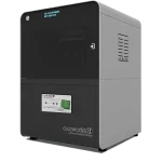
Questions on how our 3D printing system can work for your research? Connect with one of our specialists.
More Research Article Summaries
McGill University researchers build a 3D printed double-sided mold system to shape and merge brain organoids on a chip
University of Hawaiʻi researchers 3D print wearable "sweatainer" devices with true microscale internal channels
Want to read more article summaries?
We summarize the latest microfluidics and 3D printing research.
Curated from peer-reviewed publications featuring the CADworks3D system.