
Research Article Summary
5 Minute Read
University of British Columbia researchers 3D print molds to build microfluidic interfaces for silicon photonic biosensors
Title
An Optimization Framework for Silicon Photonic Evanescent-Field Biosensors Using Sub-Wavelength Gratings
Authors
Lauren S. Puumala, Samantha M. Grist, Kithmin Wickremasinghe, et al.
Journal
Biosensors (MDPI), 2022, Volume 12, Article 840
DOI Link
Summary
Puumala et al. built a two-channel PDMS microfluidic gasket from a 3D printed mold to deliver test fluid onto a silicon photonic biosensor chip, replacing a cleanroom-fabricated master mold with a benchtop, mold-and-cast workflow.

Summary Author
This page was prepared by CADworks3D to summarize and highlight a peer-reviewed research article authored by independent researchers utilizing the CADworks3D system.
Title
An Optimization Framework for Silicon Photonic Evanescent-Field Biosensors Using Sub-Wavelength Gratings
Authors
Lauren S. Puumala, Samantha M. Grist, Kithmin Wickremasinghe, et al.
Journal
Biosensors (MDPI), 2022, Volume 12, Article 840
DOI Link
Key Results at a Glance
50 µm
Print Resolution
The 3D printer reproduced the mold’s fine channel features at 50 µm resolution
~65 nm
Mold Surface Roughness
The printed mold’s surface roughness stayed low enough for PDMS to cast and release cleanly
200 x 200 µm
Channel Cross-Section
Each of the two fluid channels measured 200 µm wide and 200 µm tall over the sensor region
Zero
Release Agents Needed
PDMS demolded cleanly from the printed mold without any mold release agent
Objective
Point-of-care diagnostic tools need to be fast, low-cost, and accurate, but most existing options force a tradeoff between these goals. Lab-based blood tests give detailed results but require expensive equipment and trained staff to run in a centralized facility. Paper-based tests are cheap and portable but less sensitive. Silicon photonic (SiP) biosensors are being developed to close this gap. These are tiny optical chips, built using the same manufacturing processes as computer chips, that detect biomarkers by measuring how much a beam of light shifts as target molecules bind to the chip’s surface.
One promising SiP sensor design uses a structure called a sub-wavelength grating (SWG) waveguide, which boosts sensitivity by increasing how much light interacts with the surrounding fluid. Conventional SWG waveguides are built from isolated silicon blocks, which makes them fragile and prone to breaking apart during fabrication and testing. A newer “fishbone” SWG design links these blocks into one continuous piece of silicon, aiming to keep the sensitivity gains while fixing the fragility problem.
Testing a sensor design like this requires a reliable way to deliver fluid samples onto a chip that is only millimeters across, which typically means building a PDMS (silicone) gasket patterned with microfluidic channels. That gasket is normally cast against a master mold made in a cleanroom, a process that adds cost and turnaround time to every design iteration. This study set out to both optimize fishbone SWG biosensors and build the fluid-handling hardware needed to test them, using a 3D printed mold in place of a cleanroom-fabricated one.
Methodology and Design
The microfluidic gasket started as a two-dimensional channel layout drawn in computer-aided design (CAD) software, aligned directly to the photonic chip’s own layout so the fluid channels would line up with the sensors. This 2D pattern was extruded into a full three-dimensional mold geometry and sent to a digital light processing (DLP) 3D printer, which built the mold layer by layer from a rigid photopolymer resin. Once printed, the mold was rinsed in isopropanol, dried with compressed air, and post-cured under ultraviolet light to fully harden it before PDMS was cast against it.
This single 3D-printed mold produced two key pieces of testing hardware:
Two-Channel Gasket
Alignment Mounting Plate
Liquid PDMS was poured into the mold, slightly overfilled so its surface bulged just above the mold’s rim, then degassed in a vacuum chamber to pull out trapped air bubbles. A sheet of transparency film was laid over the mold before a weighted acrylic plate pressed the stack flat, a step that kept the finished gasket level and left its fluid through-holes fully open rather than sealed over by a thin skin of PDMS. The PDMS was then cured overnight in an oven, peeled away from the mold, and trimmed to size. Because the printed mold’s surface stayed smooth and no mold release agent was needed, the cured PDMS separated cleanly every time.
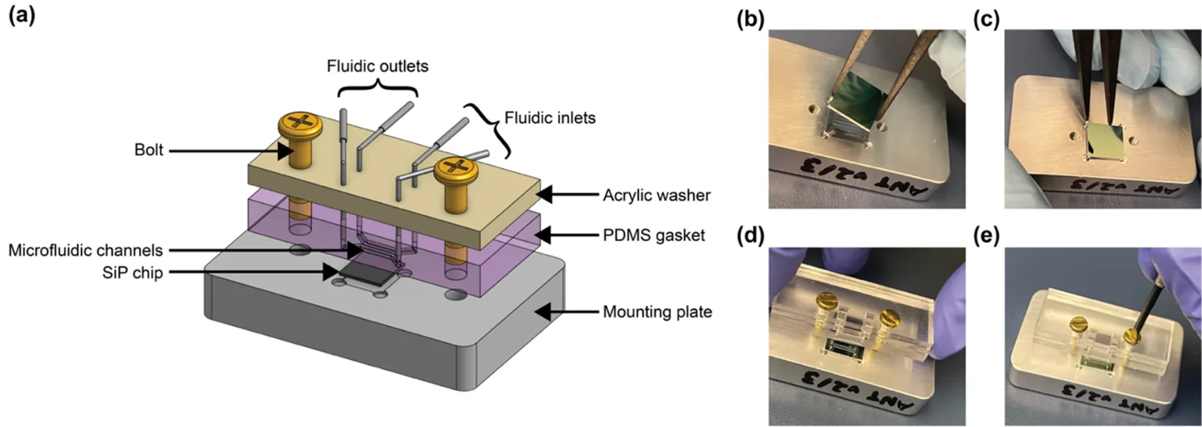
Figure 1. A schematic and step-by-step build of the 3D printed mold-based gasket assembly. (a) Schematic of the gasket seated against the photonic chip. (b) The chip is placed on the aluminum mounting plate. (c) The chip is positioned into the plate's machined recess. (d) Bolts are threaded through the acrylic washer and PDMS gasket and lined up with the plate's threaded holes. (e) The bolts are tightened, sealing the gasket against the chip without a permanent bond. Source: Puumala et al. An Optimization Framework for Silicon Photonic Evanescent-Field Biosensors Using Sub-Wavelength Gratings. Biosensors. 2022.
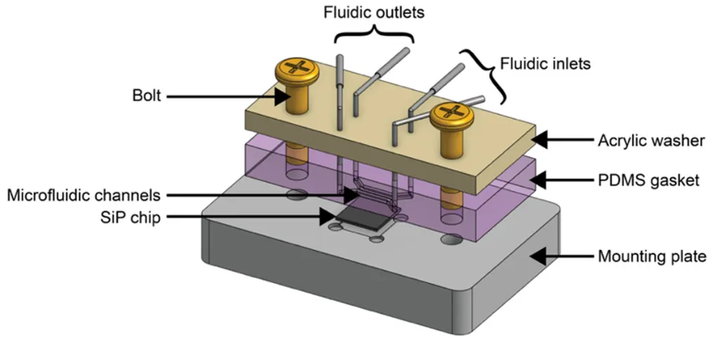
The result was a flexible gasket containing two parallel channels, each 200 µm wide and 200 µm tall, that widen into circular ports where fluid enters and exits the chip. A second, complementary piece of hardware handled alignment: the photonic chip sat in a machined recess on a custom aluminum mounting plate, with the PDMS gasket placed on top and a laser-cut acrylic washer above that. Bolts threaded through both pieces clamped everything together, pressing the gasket evenly against the chip to form a watertight seal without a permanent bond. This meant the same chip and gasket could be assembled, tested, and taken apart again for reuse.
Results
The 3D printing approach delivered the precision needed for reliable microfluidic testing. The printer reproduced the mold’s finest features at 50 µm resolution, fine enough to accurately define the 200 µm-wide channels, and the resulting mold surface had a roughness upper bound of only about 65 nm, smooth enough for PDMS to cast and release cleanly.
That clean release mattered for turnaround: because no mold release agent was required, each printed mold could go straight from post-cure to PDMS casting with no extra surface treatment step in between. The transparency-and-weight technique used during curing consistently produced flat gaskets with fully open through-holes, avoiding the thin residual PDMS membranes that can block fluid ports when a mold is only slightly underfilled.
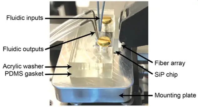
Figure 2. The completed chip-and-gasket assembly connected to fluid lines and an optical fiber array for testing, showing how the 3D printed mold-based gasket fits into a full lab setup. Source: Puumala et al. An Optimization Framework for Silicon Photonic Evanescent-Field Biosensors Using Sub-Wavelength Gratings. Biosensors. 2022.
Once assembled, the bolted mounting system held its seal through extended use. Each sensor chip was exposed to five salt solutions of increasing and decreasing concentration, repeated for a total of ten replicate exposures, without leaks or the need to re-bond the gasket to the chip between runs. This reversible, cleanroom-free assembly gave the researchers a fast way to rebuild or modify the fluidic hardware between experiments, letting the testing platform keep pace with iterations on the photonic sensor designs themselves.
“In the future, we envision that these sensors can be used for robust biosensing in applications such as the detection of cancer, inflammation, cardiac disorders, viral infection, bacteria, and toxins.”
— Puumala et al., An Optimization Framework for Silicon Photonic Evanescent-Field Biosensors Using Sub-Wavelength Gratings. Biosensors. 2022.
Products Used In This Study

Questions on how our 3D printing system can work for your research? Connect with one of our specialists.
More Research Article Summaries
McGill University researchers build a 3D printed double-sided mold system to shape and merge brain organoids on a chip
University of Hawaiʻi researchers 3D print wearable "sweatainer" devices with true microscale internal channels
Want to read more article summaries?
We summarize the latest microfluidics and 3D printing research.
Curated from peer-reviewed publications featuring the CADworks3D system.