
Research Article Summary
5 Minute Read
Université Laval researchers build a field-portable cell-sizing sensor using a 3D printed mold for rapid PDMS microchannel fabrication
Title
Portable Impedance-sensing device for microparticle characterization
Authors
Karim Bouzid
Journal
Master’s thesis, Maîtrise en génie électrique, 2022
DOI Link
Summary
Bouzid et al. developed a portable impedance flow cytometry device that detects and sizes microparticles directly in the field, pairing low-cost PCB electronics with a PDMS microchannel cast from a stereolithography 3D printed mold. The approach swaps slow, cleanroom-bound microfabrication for a fast, benchtop molding workflow that any well-equipped lab can run.
Summary Author
This page was prepared by CADworks3D to summarize and highlight a peer-reviewed research article authored by independent researchers utilizing the CADworks3D system.
Title
Portable Impedance-sensing device for microparticle characterization
Authors
Karim Bouzid
Journal
Master’s thesis, Maîtrise en génie électrique, 2022
DOI Link
Key Results at a Glance
2,238
Microparticles Characterized
Beads were detected and sized across a multi-curve dataset
50–90 µm
Detected Size Range
Reliable diameter readout for beads above 50 µm
90 µm
Smallest Printed Channel
Minimum defect-free channel width achieved in the mold
Over 98%
Impedance Percision
Magnitude and phase error after calibration
Objective
Counting and sizing single cells or microparticles usually means sending samples to a lab stocked with bulky flow cytometers and trained operators. That works in a hospital or a university core facility, but it falls apart the moment you need an answer in the field, at a remote water source, a farm, or a clinic with no benchtop instrumentation. The researchers set out to close that gap with a device small enough to carry, cheap enough to deploy widely, and simple enough to operate without specialist training.
The sensing principle they chose is impedance flow cytometry. When a particle suspended in a conductive liquid passes between a pair of electrodes, it briefly displaces some of that liquid and changes the electrical impedance the electrodes measure. The size of that change scales with the size of the particle, and the time it takes to cross a known electrode gap reveals how fast it is moving. Because the method reads an electrical signal rather than a fluorescent tag, it needs no dyes, no lasers, and no optical alignment, which is exactly what makes a portable, label-free instrument realistic.
The harder problem sits upstream of the electronics: the microfluidic channel itself. A channel that guides particles single-file past the electrodes typically has internal features measured in tens of µm, and the conventional way to make one is soft lithography. That process relies on a photolithographically patterned silicon master produced in a cleanroom, which is slow, expensive, and out of reach for most teams that would benefit from a portable sensor. If the goal is an instrument that labs can build and iterate on themselves, the channel has to come from a faster, lower-barrier process. The gap this work addresses is therefore as much about manufacturability as it is about sensing: how do you fabricate a precise PDMS microchannel quickly, on a benchtop, without a cleanroom, and still get a channel clean enough to do quantitative single-particle measurements?
Methodology and Design
The fabrication route replaces the cleanroom master with a printed one. The channel geometry is drawn as a solid model in CAD software, exported as an STL file, and printed on a stereolithography resin printer using a resin formulated specifically for casting silicone parts. Printing the negative of the channel directly is what removes the photolithography step entirely: the feature that would normally require a patterned silicon wafer is simply printed, then cast in PDMS and sealed against the sensing electrodes to form a reusable cartridge.

Figure 1. The benchtop fabrication route: liquid PDMS is poured into the 3D printed mold, cured at 70 °C, peeled off, plasma-bonded, and sealed against the electrode board. Source: Bouzid, Université Laval, 2022.
That pipeline comes together in four core components:
Impedance Flow Cytometer
PDMS Microchannel
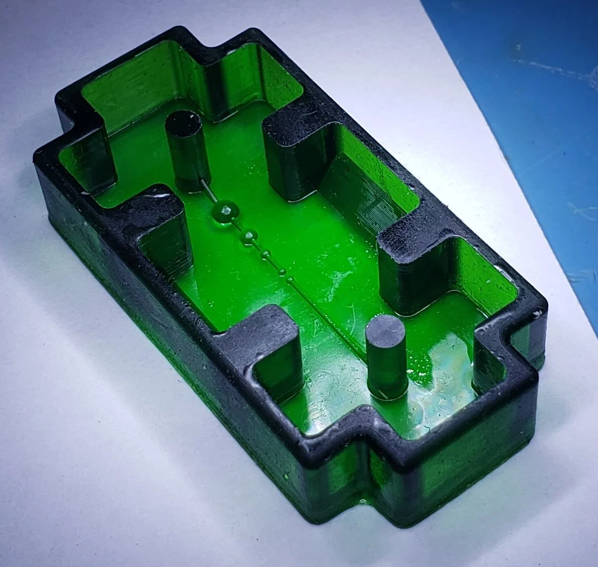
3D-Printed mold
3D-Printed Squeezers
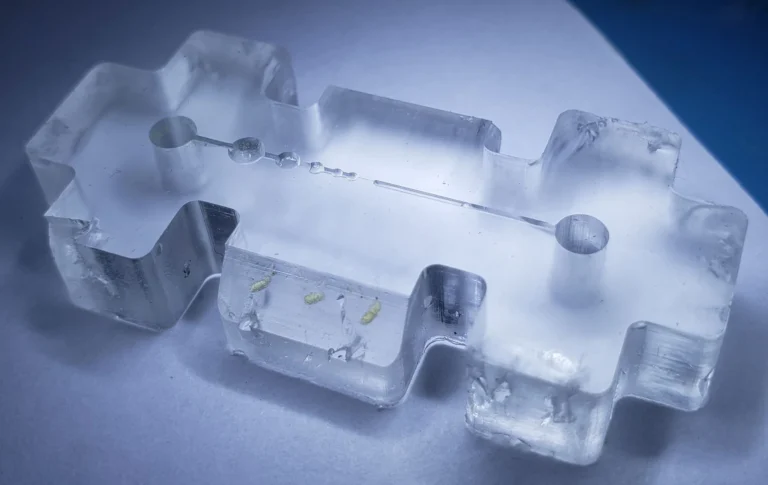
Figure 2. The finished PDMS channel released from the mold (left) with a microscope view of the molded microchannel (right). Source: Bouzid, Université Laval, 2022.
The impedance flow cytometer sits at the center of the device, using patterned electrodes on a single-layer PCB to size particles as they pass through the channel. The PDMS microchannel guides the sample past those electrodes, its geometry cast directly from the printed mold so no cleanroom fabrication is needed. The 3D printed mold is what makes that casting possible, since printing the channel’s negative geometry replaces the patterned silicon wafer a cleanroom process would normally require, letting the same channel design be reproduced directly from a resin printer. Holding everything together are two 3D-printed squeezers, which clamp the PDMS channel against the electrode board to seal the system without adhesives or permanent bonding, keeping the cartridge reusable rather than disposable.
Casting follows standard PDMS practice. The silicone base and curing agent are mixed at 10:1, degassed for about an hour to pull out air bubbles, poured into the mold, and baked on a hotplate at 70 °C for 50 minutes, with an overnight dwell at 40 °C. The cured channel is then gently lifted from the mold with a scalpel. To make the channel walls reliably wettable, the PDMS surface is treated with plasma and immediately coated with PEG to hold its hydrophilicity, then briefly baked again.
Sealing the channel against its sensing electrodes is handled mechanically rather than with permanent bonding. The patterned electrodes live on a single-layer PCB whose outline matches the channel, so the two stack in registration. Two printed squeezers sandwich the PDMS channel and the electrode board and are drawn together with screws; because PDMS is soft, that clamping pressure forms a hermetic seal on its own. Tubing pressed into the inlet and outlet completes the assembly, and a programmable syringe pump drives sample through at a controlled rate. The result is a sealed, reusable cartridge that can be opened, cleaned, and reassembled, which is far more practical for fieldwork than a single-use bonded chip.
The final device is a tree-like concentration gradient generator splits and recombines two inlets across six outlets, producing a stable, stepped gradient for applications in drug-dosing studies.
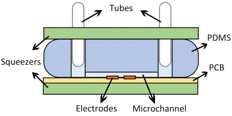
Figure 3. Cross-section of the sealed cartridge: printed squeezers clamp the PDMS channel onto the PCB electrodes, with tubing at the inlet and outlet. Source: Bouzid, Université Laval, 2022.
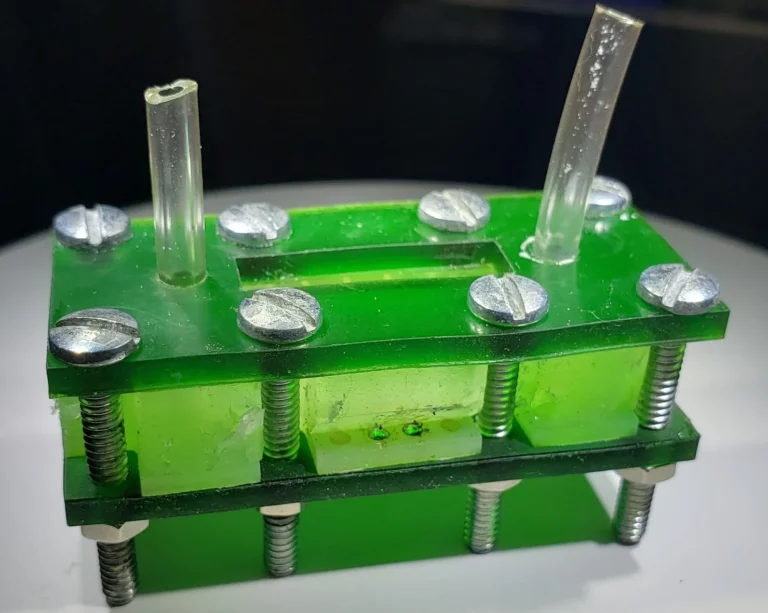
Figure 4. The fully assembled microfluidic cartridge, PDMS channel, electrode board, printed squeezers, tubing, and screws ready to run sample. Source: Bouzid, Université Laval, 2022.
Results
The printed-mold route produced channels good enough for quantitative work. The printer’s theoretical resolution is around 30 µm, and in practice the team found that the smallest channel they could print without major defects was 90 µm wide, a useful benchmark for anyone planning feature sizes against this kind of resin and printer. Cast and sealed, the system ran sample reliably and held together without leaks under syringe-pump pressure.
On the sensing side, the device delivered the precision needed for single-particle sizing. After calibration, impedance magnitude and phase were both measured to within less than 3%, and the instrument operated across an excitation range of roughly 30 kHz to 15 MHz. Working with polyethylene beads suspended in saline, the sensor cleanly resolved individual particles, and could even distinguish air bubbles, which produced very large impedance spikes, from genuine bead events.
The scale of the demonstration is what shows the approach is more than a one-off. From a set of seven recordings, the detection and classification pipeline picked out 2,238 individual microbeads and estimated each one’s diameter and velocity. Reliable detection spanned roughly 50 µm to 90 µm; beads smaller than 50 µm slipped below the sensor’s sensitivity floor, which sets a clear lower bound for this electrode geometry. Taken together, the results show that a benchtop, cleanroom-free fabrication route can produce microchannels precise enough to support thousands of quantitative single-particle measurements, the kind of throughput that makes downstream data analysis worthwhile.
“Printing the channel’s negative directly turns a cleanroom-scale fabrication problem into a benchtop one, fast enough to redesign and recast in a single day.“
— Summary of the fabrication approach in Bouzid, Université Laval, 2022.
Products Used In This Study

Questions on how our 3D printing system can work for your research? Connect with one of our specialists.
More Research Article Summaries
McGill University researchers build a 3D printed double-sided mold system to shape and merge brain organoids on a chip
University of Hawaiʻi researchers 3D print wearable "sweatainer" devices with true microscale internal channels
Want to read more article summaries?
We summarize the latest microfluidics and 3D printing research.
Curated from peer-reviewed publications featuring the CADworks3D system.